
Electrolyte Influence on Properties of Ultra-Thin Anodic Memristors on Titanium
by
 , and
, and
Dominik Knapic
1,
Elena Atanasova
1,
Ivana Zrinski
1,
Achim Walter Hassel
1,2 and
Andrei Ionut Mardare
1,* 1
Institute of Chemical Technology of Inorganic Materials, Johannes Kepler University Linz, Altenberger Str. 69, 4040 Linz, Austria
2
Faculty of Medicine and Dentistry, Danube Private University, Steiner Landstraße 124, 3500 Krems an der Donau, Austria
*
Author to whom correspondence should be addressed.
Coatings 2024, 14(4), 446; https://doi.org/10.3390/coatings14040446
Submission received: 12 March 2024
/
Revised: 4 April 2024
/
Accepted: 6 April 2024
/
Published: 9 April 2024
(This article belongs to the Special Issue Thin Films and Nanostructures for Electronics)
Abstract
:Titanium anodic memristors were prepared in phosphate buffer (PB) and citrate buffer (CB) electrolytes. Studying their I-U sweeps, the memristors presented self-rectifying and volatile behaviors. Transmission electron microscopic analysis revealed crystalline protrusions inside a semi-crystalline Ti oxide. Grounded in this, a hybrid interfacial memristive switching mechanism relaying on partial filaments was proposed. Moreover, both analyzed memristor types demonstrated multilevel switching capabilities. The memristors anodized in the PB and CB showed high-to-low resistance ratios of 4 × 10⁴ and 1.6 × 10², respectively. The observed (more than two order of magnitude) ratio improvement of the PB memristors suggests their better performance, in spite of their modestly high resistive state instabilities, attributed to the thermal stress caused by consecutive switching. The endurance and retention of both the PB and CB memristors was measured over up to 106 cycles, indicating very good lifetimes. Phosphate incorporation into the anodic oxide was confirmed by photoelectron spectroscopy analysis and was related to the improved memristive behavior of the PB sample. The presence of phosphate inside the memristively active layer modifies the availability of free O species (vacancies and ions) in the oxide. Taking all this into consideration, Ti anodic memristors anodized in PB are emphasized as candidates for neuromorphic computing.
1. Introduction
In recent years, there has been a notable increase in thin film research activities within the field of complementary metal–oxide–semiconductor (CMOS) technology and associated architectures, including memristors. The memristor, a fundamental fourth circuit element apart from the inductor, capacitor and resistor, was initially conceptualized by Chua in 1971 and experimentally developed by HP laboratories more than three decades later [1,2]. Recently, the reported anodic memristors studies increased in number, suggesting an increased scientific interest [3]. The oxide, which is the active material within a metal–insulator–metal (MIM) structure, is produced by anodization, where the metallic bottom electrode is the anode [4,5]. Anodization is a rather straightforward process that is not very energy intensive and does not require an ultra-high vacuum, which is beneficial for the ease of the production process. In anodic memristor production, the anodization process is the one that defines the electrical properties [6]. By changing the anodization parameters such as the electrolyte, scan rate and maximum potential, the oxide has different characteristics that directly impact the electrical behavior of the memristor. These parameters can be tuned to intrinsically produce memristors with desired properties such as improved stability, endurance and retention [6,7,8].
Titanium-based anodically prepared memristors were reported to show self-rectifying properties [7]. Self-rectifying memristors have an integrated one-rectifier (diode)–one-memristor (1D1M) configuration [9]. In this case, a diode is an integrated rectifier, which is formed at the top electrode/oxide interface due to the formation of a Schottky barrier. Self-rectifying memrsitors have also shown volatile behaviors [2,10,11]. Volatile memristors [12] may be further categorized as digital (threshold), with abrupt switching for on/off processes, and analog, with a gradual switching [4]. Digital memristors typically have a filamentary switching mechanism, while analog devices have a non-filamentary one based on an interfacial switching mechanism [11,13]. Depending on their unique resistive switching properties, such as volatile or non-volatile and digital or analog behavior, memristors are utilized for various use-cases such as image processing [14,15], sensing of OH− species [16,17,18], memory [19,20,21,22] or neuromorphic computing [23,24,25,26,27,28].
Non-volatile memristors emulate the biological functions related to long-time memory and information storage, whereas volatile memristors mimic the biological process of learning and forgetting associated with the short-term memory [12,27]. The volatile resistive switching characteristic makes them ideal for applications in synaptic devices for neuromorphic computing, modeling nociceptors and serving as physical reservoirs in computing for the management of time-specific data [23,29,30]. In the context of brain architecture, synapses describing two-terminal structures connecting neurons are effectively mimicked by memristors in artificial neuromorphic networks [12,27].
In the current study, Ti anodic memristors were prepared in two different electrolytes, 1 M phosphate buffer (PB) and 0.1 M citrate buffer (CB). The motivation for this was to describe the influence of electrolyte incorporation into the growing oxide [6,8,31,32] on the electrical properties of the resulting memristors. To electrically characterize the memristors, the memristive retention (reading process) and endurance (writing process) were analyzed, while the predominant conduction mechanism was determined based on I-U sweeps. The electrolyte species incorporation was studied by X-ray photoelectron spectroscopy (XPS). To gain better insight into the switching mechanism, the memristors were studied by cross-sectional transmission electron microscopy (TEM) at atomic scale.
2. Materials and Methods
2.1. Fabrication of Ti Anodic Memristors
The deposition of the Ti thin film was carried out through magnetron sputtering in an ultra-high vacuum system (Mantis Deposition, Thame, UK) with a base pressure within the 10−6 Pa range. A Ti film of approximately 300 nm thickness was sputtered onto a thermally pre-oxidized Si wafer, utilizing a high-purity Ti target (99.95%, Demaco Holland BV, Noord-Scharwoude, The Netherlands). This process was conducted at ambient temperature in an Ar atmosphere, maintaining a pressure of 5 × 10⁻¹ Pa and employing a DC power setting of 80 W. The sample was rotated at a speed of 5 rpm during deposition to ensure the uniformity of the film thickness across the substrate.
After the deposition of the Ti film, the substrates underwent electrochemical anodization in room temperature conditions using a 0.1 M CB solution [33] and a 1 M PB solution [34]. The growth of the anodic oxide was performed by potentiodynamic anodization at a rate of 100 mV s−1, reaching up to 8 V (versus the SHE). For this procedure, a CompactStat potentiostat (Ivium Technologies BV, Eindhoven, The Netherlands) was utilized in a three-electrode setup. This setup included Ag|AgCl|3 M KCl as the reference electrode, a Pt mesh as the counter electrode and the Ti thin film as the working electrode. Following the formation of the anodic oxide on the Ti thin films, the substrate was reintroduced into vacuum to pattern the top electrodes. This was achieved by utilizing a Ni shadow mask foil, which was positioned in direct contact with the surface of the Ti oxide. The construction of the memristive devices was completed by depositing 150 nm thick Pt electrodes, each 200 µm in diameter, using sputtering from a target of high purity (99.95%, MaTeck, Jülich, Germany) in an Ar atmosphere at ambient temperature.
2.2. Electrical Characterization
Electrical measurements were conducted using an electrical setup consisting of a Keithley 2450 SourceMeter Unit (SMU), which was interfaced with a self-developed Gantry robot. This robot, featuring high-precision XYZ translation stages, was outfitted with dual microscope cameras from Bresser, Germany, enabling the observation of the Pt top electrodes from both a top (normal) and a side (45° angle) perspective. A W needle with a tip diameter of 10 µm mounted on the Z stage through a force sensor, was employed for making gentle contact with the memristor’s top electrode, maintaining a constant force of 10 ± 1 mN. The Ti bottom metal electrode made ohmic contact with a stainless steel needle positioned at the Si wafer’s edge, directly contacting the thin film. The entire setup was operated through self-developed LabView® software (https://www.ni.com/), designed for executing current–voltage (I-U) sweeps, along with endurance and retention evaluations. These procedures were all carried out under standard conditions, applying voltage to the Ti bottom electrode while grounding the top Pt electrode. The SMU was utilized to record the I-U sweeps, with the compliance current adjusted within the milliampere range. Endurance and retention trials were conducted at 260 Hz for up to 106 cycles, initially biasing the memristors at voltages that facilitate switching between the low resistance state (LRS) and high resistance state (HRS).
The resistance of the device was always determined by applying a voltage of 0.01 V. The LRS was identified at the lowest resistance encountered during the SET or RESET processes, while the HRS was determined at the highest resistance value, measured at 0.1 V. The SET and RESET voltages (Uset and Ureset) varied from ±3 to ±6 V, respectively.
2.3. XPS and TEM Analysis
The chemical composition of the memristive anodic oxides was examined using a NEXSA G2 XPS system from Thermo Scientific, Pardubice, Czech Republic, utilizing for operation the Avantage software package (https://www.thermofisher.com) by Thermo Scientific, Winsford, UK. The analysis involved the use of monochromated Al Kα X-ray radiation (1486.6 eV), with any resulting surface charge neutralized by a dual flood gun. Survey spectra were captured at a pass energy of 200 eV and an energy step of 1 eV, while high-resolution spectra were obtained with a pass energy of 20 eV and a step energy of 0.05 eV. To correct for charge shifts, all the spectra were aligned using the C1s peak of adventitious C at 285.0 eV. Angle-resolved XPS (AR-XPS) analyses were conducted on a Theta Probe XPS system by Thermo Scientific, Winsford, UK, which is equipped with a 2-D detector allowing for measurements without sample tilting. These spectra were acquired with a pass energy of 50 eV and a binding energy step of 0.05 eV. The spectrometer’s acceptance angle, which ranges from 20° to 80°, was divided into eight angle intervals, each separated by 7.5°.
The Ti thin film’s surface microstructure was examined using a field emission scanning electron microscope (FE-SEM, Leo 1550 VP Zeiss, Oberkochen, Germany), with images captured at an acceleration voltage of 3 kV utilizing the in-lens detector. To elucidate the structure and chemical composition at the nanometer scale, cross-sectional transmission electron microscopy (TEM) analysis was employed. This was conducted using a JEOL JEM-2200FS (JEOL Inc., Tokyo, Japan) microscope, operated at 200 kV. This TEM features an in-column Omega filter and a TemCam-XF416 (TVIPS, Gauting, Germany) CMOS camera for imaging, with images captured using zero-loss filtering. The preparation of cross-sectional lamellae for examination was performed using focused ion beam (FIB) milling with a CrossBeam 1540 XB (Zeiss, Oberkochen, Germany). To safeguard the surface during preparation, samples were initially coated with a Pt deposit by an electron beam, followed by deposition of a Pt layer by ion beam to act as a protective sacrificial layer. For the qualitative analysis of the elements, energy-dispersive X-ray spectroscopy (EDX) was carried out in the scanning (S)TEM mode, using an X-MaxN 80 T detector by Oxford Instruments Ltd., Abingdon, UK, with data analysis conducted through the Aztec software (https://www.aztecsoftware.com/) specifically designed for this purpose.
3. Results and Discussion
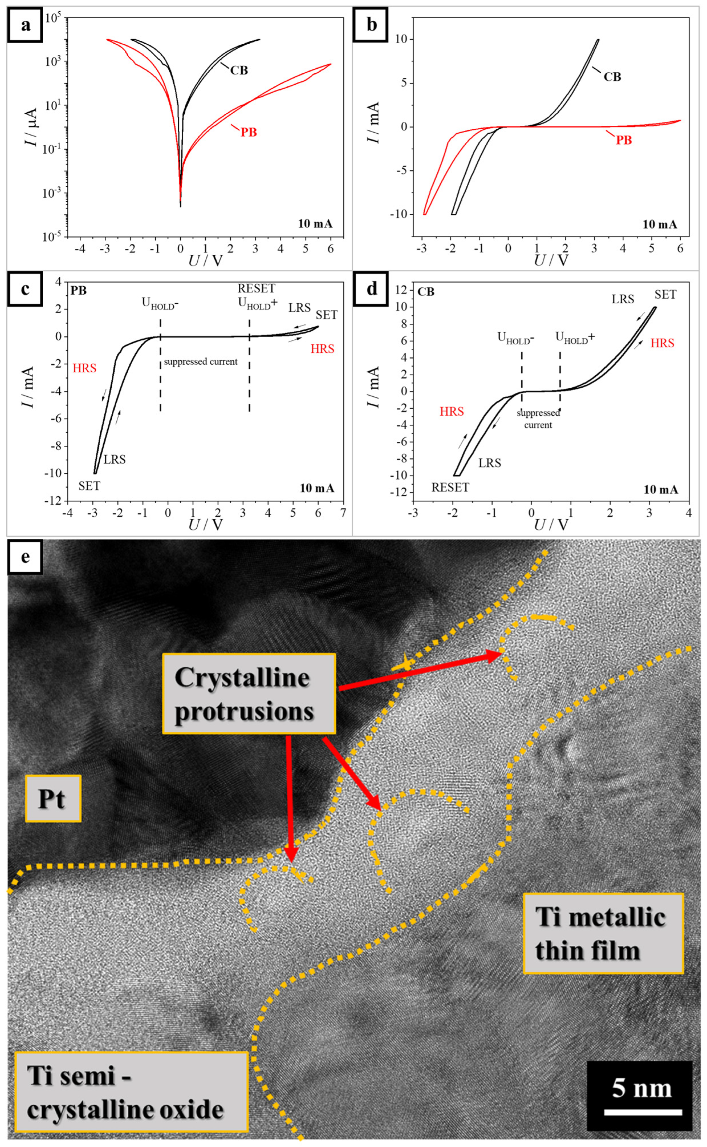
Two variations of the Ti anodic memristors were fabricated, one anodized in PB and the other in CB, in order to investigate the influence of the electrolyte used for anodization on the electrical properties of the memristors. Figure 1 shows the I-U sweeps of the memristors prepared in the PB and CB, together with the TEM analysis. Figure 1a,b show the direct comparison of the representative memristors anodized in the PB and CB in logarithmic and linear current scales, respectively. The curves have a typical shape describing analog interfacial memristors. Their typical characteristic is the suppressed current defined by the hold voltage and the gradual transition from the HRS to the LRS and vice versa [35,36]. Both memristors show a self-rectifying behavior defined by a strong current suppression [23,37,38].
The self-rectifying memristor performs similarly to a 1D1M device by integrating a Schottky barrier at one of the MIM interfaces with the active memristive layer [7,36,37,39]. In this study, this characteristic is inherently achieved through the fabrication process, which includes the anodic oxidation of the Ti bottom electrode, and subsequent deposition of the Pt top electrode. Consequently, the Schottky barrier is formed at the Pt/Ti oxide interface. The primary function of the 1D1M device lies in its ability to inhibit sneak current pathways in crossbar array architectures. When this characteristic is paired with the volatile behavior of the memristors under investigation, the Ti anodic memristors emerge as highly suitable for applications in neuromorphic computing [30,39,40,41].
The exemplified memristors are further analyzed in more detail in Figure 1c,d. Figure 1c presents the I-U sweep of the memristor anodized in the PB. Initially, the memristor finds itself in the HRS. By sweeping to the positive voltage, the current is suppressed up to approximately U = 3 V, where the UHOLD+ value is thus defined. Further increasing the voltage, the current slightly increases by finally reaching the USET value, which is defined as the voltage where the HRS is switched to the LRS. By sweeping the potential in the opposite direction, the current is again suppressed at UHOLD+, where it also switches back to the HRS, thus defining the RESET value. This is seen better in Figure 1a at approximately U = 3 V. Further lowering the voltage to the negative values, the current starts increasing again at UHOLD− = −0.3 V until finally reaching the USET value at −3 V, where it switches back to the LRS.
Figure 1d presents the I-U sweep of the memristor anodized in the CB. Similar to the case of the memristor produced in the PB, the initial state of the CB memristor is the HRS. The current is suppressed until UHOLD+ = 1 V. As the voltage is further swept in the positive direction, USET is reached at 3 V, where it switches to the LRS. By sweeping the voltage in the opposite direction, the current is again suppressed when it reaches 1 V. Further, the current suppression is visible until UHOLD− is reached at −0.3 V. The negative current reaches its maximum at URESET = −2 V, where the LRS switches to the HRS. There are some obvious differences when comparing the I-U sweeps of the PB and CB samples. The I-U sweep of the memristor anodized in the PB has a much larger suppressed part of the current and the current at the positive side of the curve does not reach values higher than 1 mA. On the contrary, the I-U sweep of the memristor anodized in the CB shows a much smaller suppression part and the current reaches an absolute value of maximum 10 mA in both the positive and negative parts. Moreover, the PB sample has two SET values at the positive and negative sides of the voltage and a RESET at the hold value on the positive side, while the CB sample has a SET value at the positive side and RESET at the negative side of the curve. The memristor prepared in the PB shows a stronger asymmetry when compared to the one prepared in the CB.
Figure 1e shows a TEM image of the MIM structure of the memristor anodized in the PB. The TEM analysis was conducted only for the PB sample as it showed superior performances as compared to the CB sample. On Figure 1e, crystalline protrusions (highlighted in orange) are seen inside the amorphous oxide layer. Following the TEM analysis, a hybrid interfacial resistive switching mechanism is proposed, where only partial filaments are formed. The crystalline protrusions observable in the figure act as preferential paths for the partial filament formation [42,43]. They do not reach all the way through the oxide, so there is no full filamentary switching. The partial filaments, therefore, simulate an effective bottom electrode. Interfacial memristors exhibit resistive switching due to O species migration, including ions and vacancies, that are distributed through the entire interface [13,36,42,43]. This switching mechanism is based on the Schottky-like barrier formation, which can be modulated by varying the O species concentration [36,44]. The presence of an electric field increases the concentration of vacancies at the interface, reducing the barrier height and thus transitioning the device to a low resistance state. Conversely, the concentration of O vacancies decreases due to the electric field reversal, resulting in an increased barrier height, reverting the device to a high resistance state [36,42]. The initial electron trapping at the Pt/oxide interface is reported to create a negatively charged layer, prompting the accumulation of O vacancies in the nearby depletion zone to counterbalance this charge [13,36]. The different asymmetry of the I-U sweep for the memristor prepared in the PB and CB can be explained by different depletion dynamics and the amount of O vacancies in the Schottky barrier, which could be a result of phosphate incorporation into the oxide [13,36,42].
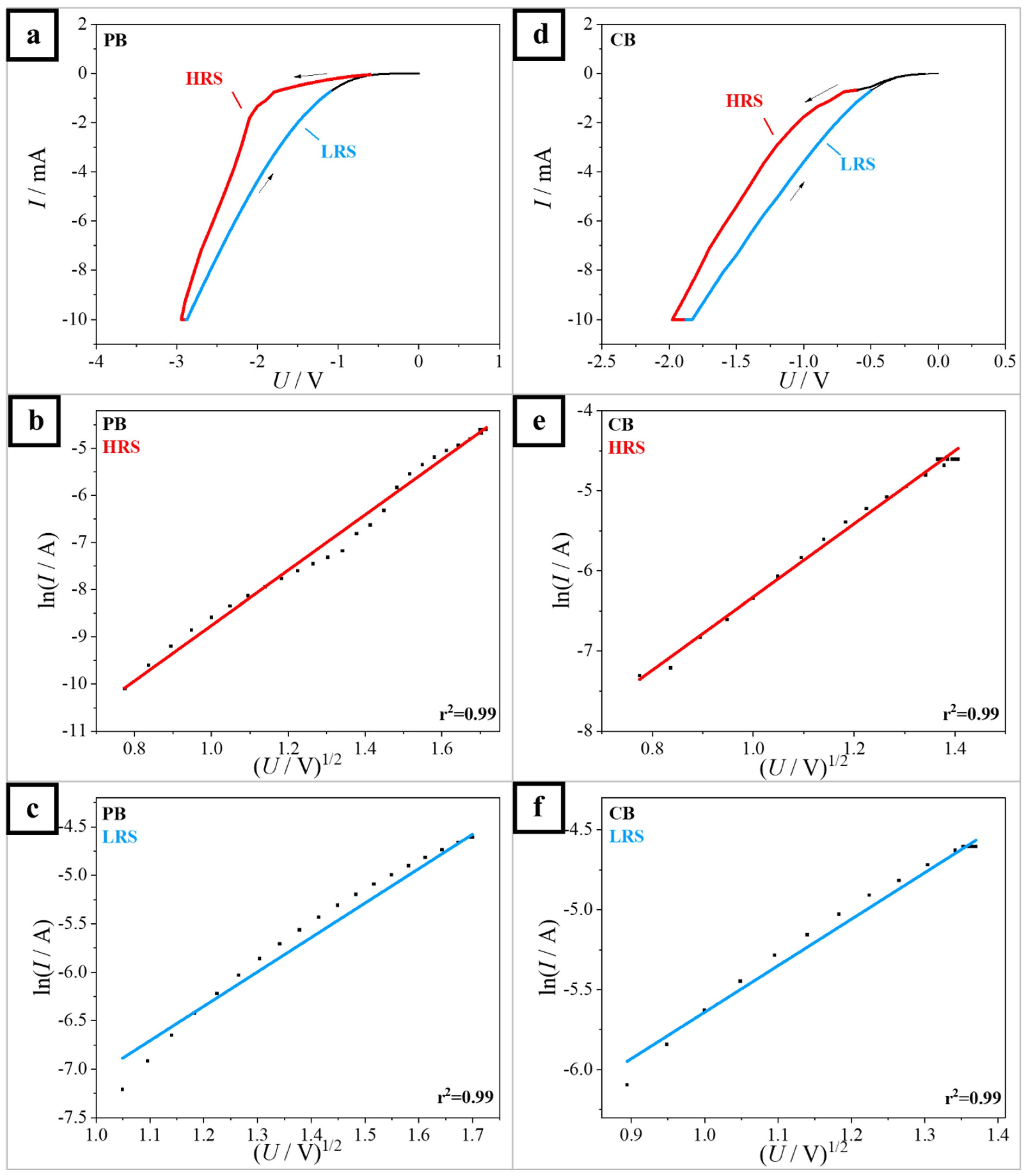
To strengthen the argument for the proposed switching mechanism, a conduction mechanism analysis was performed and the obtained results are summarized in Figure 2. Figure 2a,d show the selected regions of the I-U sweeps that were analyzed. Parts (b) and (e) of the figure show the analysis of the HRS regions, while (c) and (f) present the data for the LRS analysis of the PB and CB samples, respectively. Generally, when a linear regression is established on a ln(I/A) vs. (U/V)1/2 plot, the Schottky emission is concluded as the dominant conduction mechanism [45,46,47]. Analyzing the plots of the HRS and LRS for both the PB (b,c) and CB (e,f) samples, as shown in Figure 2, the Schottky emission is revealed as the dominant conduction mechanism. The Schottky emission is a thermionic process in which electrons are injected into the conduction band of the oxide by overcoming an energy barrier through thermal activation [46]. The Schottky or thermionic emission is often observed as the dominant conduction mechanism in metal oxides and it was already reported for similar memristors [46,48,49] including Ti/TiO2 [38]. Hence, in the present study, the Schottky emission is safely concluded to be the dominant conduction mechanism, confirming the suggested memristive switching mechanism.
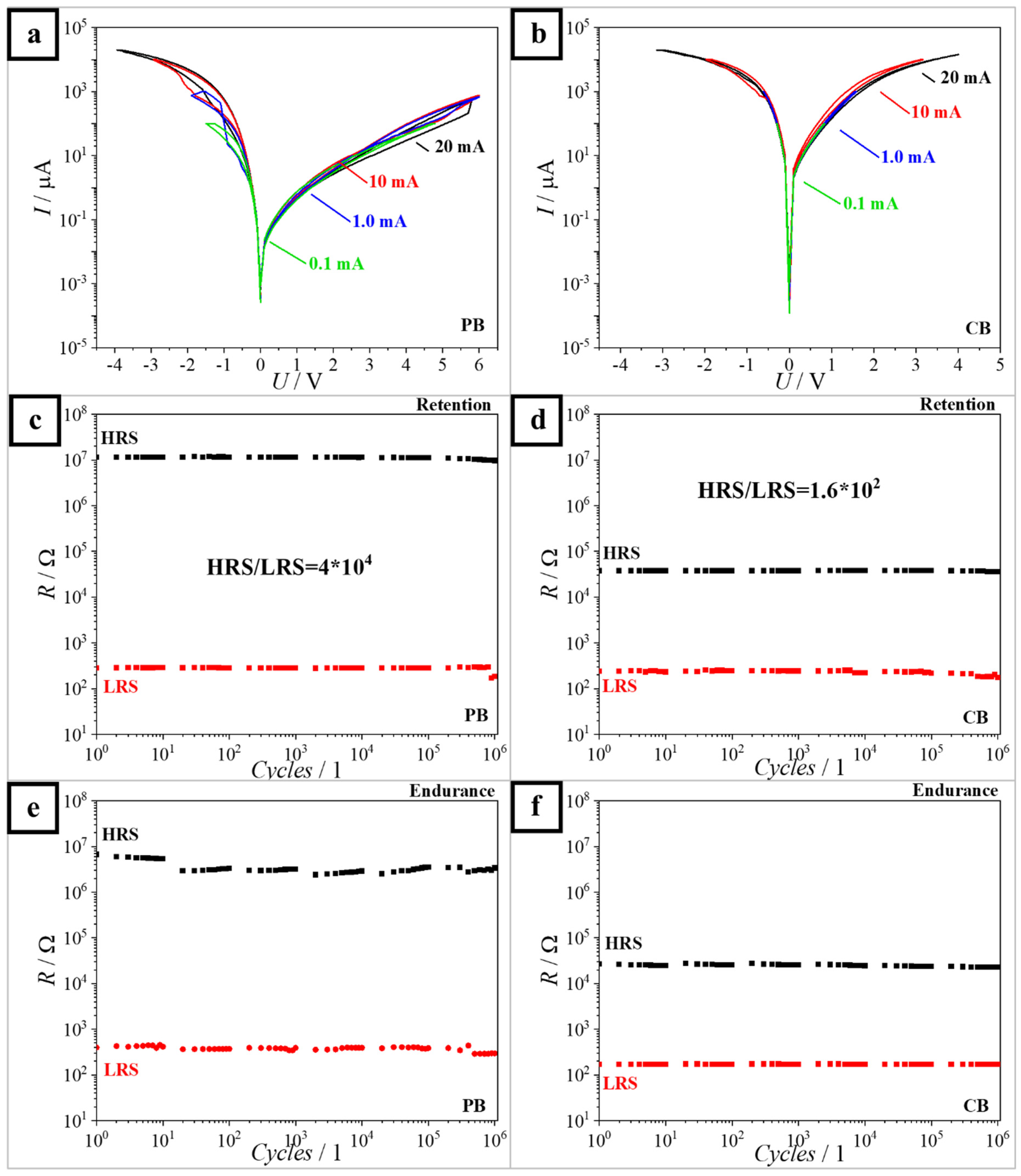
In Figure 3a,b, the I-U sweeps measured with different current compliances are presented. It can be seen that by changing the current compliances, the SET and RESET values also change. This phenomenon is described as multilevel switching [42,50], involving a filamentary switching mechanism in which various simultaneous conductive filaments (CFs) lead to different resistance states [8]. Although multilevel switching has usually been reported for filamentary memristors, there have been reports of multilevel switching for interfacial, non-filamentary memristors as well [23,42]. The multilevel switching observed in the interfacial memristors results from the variation of O vacancy concentrations at the interface [36]. The multilevel switching is a crucial feature of applications in neuromorphic systems. This tunability across multiple resistance levels significantly enhances the plasticity of electronic synapses equivalents in artificial neural networks. Additionally, the capability for multilevel switching in resistivity levels allows the storage of more than 2 bits within a single unit, which enables high-density and robust neural networks [38,39].
The memristors analyzed in this work were characterized by reading and writing procedures to determine their retention and endurance capabilities. Figure 3 displays the retention and endurance data of memristors prepared in the PB (Figure 3a,c) and CB (Figure 3b,d). The memristors prepared in both the PB and CB showed good retention by holding stable values of the HRS and LRS up to 106 cycles. Comparing the HRS/LRS ratios for the PB and CB memristors, a significant difference is observed. The HRS/LRS values measured for the PB memristors was 4 × 10⁴ and for the CB memristors was 1.6 × 10². This is explained by higher oxide resistance for the memristors prepared in the PB, confirming previous reports [6,32]. The endurance measurement of both the PB and CB memristors showed a lifetime of 106 cycles. During the initial writing experiments, it was found that both memristors show volatile behavior by not remembering the resistive state when the reading voltage was applied. Therefore, the writing experiments were performed by reading the resistance values at the switching voltages. Analyzing the endurance of the PB memristor, it can be seen that the HRS values are unstable compared to the HRS of the CB memristor. The HRS values showed instabilities after each I-U sweep at the beginning of a decade and they increase slightly during each decade, showing lower values at the start of the decade and higher values at the end of the decade. This can be explained by thermal stress in the oxide, which is causing instability in the resistance values [13].
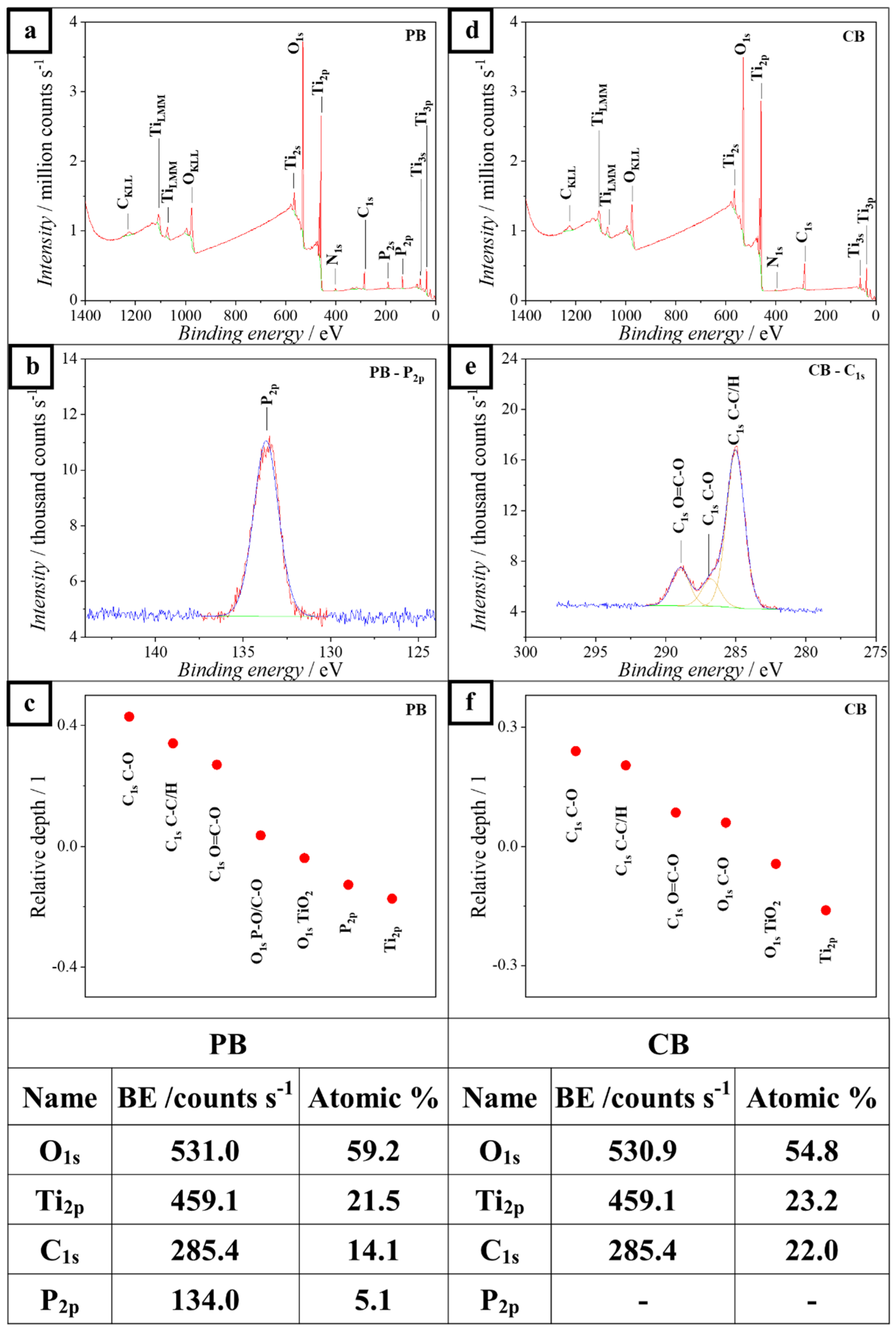
In order to link the incorporation of electrolyte species into anodic oxides with their memristive behavior, a chemical analysis study was performed by XPS. Figure 4 shows the results obtained from the memristive oxides prepared in the PB (a,b) and CB (d,e). Additionally, a relative depth analysis is presented in Figure 4c,f. The table attached to Figure 4 shows the obtained oxide compositions for the PB and CB samples. A peak at BE = 531 eV for O1s was detected for both samples and is attributed to the TiO2 [51]. As seen in the table, the relative composition of O for the PB sample was 59.2% and for the CB sample was 54.8%. Next, the Ti2p peak, which also corresponds to TiO2 [52], was also found in both samples. The Ti relative composition amounted to 21.5% for the PB and 23.2% for the CB sample. Moreover, in both samples a C1s peak at BE = 285.4 eV was detected and its detailed spectra are shown in Figure 4e. This C1s peak could be associated with citric acid [53] and various organic compounds, including contaminations. The measured C relative composition was 14.1% for the PB sample and 22% for the CB sample. In order to investigate the possible citrate incorporation into the anodic oxide, the relative depth distribution was assessed by means of angle-resolved XPS (Ar-XPS). The relative depth plots (Figure 4c,f) were calculated from the AR-XPS data by taking the logarithm of the ratio between the bulk-sensitive angles and the surface-sensitive angles [54,55]. It was found that, for both samples, the C-based species were observed only at the surface, which indicates that there was no remarkable citrate incorporation. The absence of citrate incorporation in the anodic Ti oxide was already reported in previous studies [31]. For the PB sample, a P peak at BE = 134 eV was clearly identified, as seen in Figure 4b. The P2p peak describes the phosphate ion PO43− [56]. As seen in the table, the P content was measured at 5.1% for the PB sample, while for the CB sample there was no P signal detected. This describes the phosphate ion incorporation into the memristive active layer due to the anodic oxidation in the 1 M phosphate buffer, confirming previous reports [6,8,31,32,57].
Similar to the CB case, the electrolyte phosphate incorporation was demonstrated by analyzing the relative depth distribution at different angles (Figure 4c). The phosphate was found at a depth below the surface close to the position of the Ti and below that of the TiO2, which confirms the incorporation and excludes a superficial adherence due to electrolyte exposure to phosphate species during anodization. Phosphate incorporation can justify the discussed difference in the asymmetry of the I-U sweeps between the PB and CB samples (see Figure 1). This can also be responsible for different amounts of the O species, which can be depleted inside the Schottky barrier, leading to different I-U sweep behaviors and different HRS/LRS ratios. Overall, the electrolyte incorporation is at least as reproducible as the anodization itself, since it relies on the same driving force provided by the high electric field applied.
4. Conclusions
In this study, the characterization of Ti-based anodic memristors anodized in PB and CB was successfully performed. The memristors prepared in both the PB and CB showed self-rectifying properties. They were characterized and classified as analog volatile interfacial memristors. TEM analysis revealed crystalline protrusions inside of the semi-crystalline Ti oxide. According to this analysis, a hybrid interfacial memristive switching mechanism was proposed. This is based on partial filaments and varying the Schottky barrier height due to the depletion of the O species combined with electron trapping and de-trapping. Moreover, the Schottky emission was confirmed as the dominant conduction mechanism, which is in agreement with the proposed switching mechanism. Furthermore, by studying the I-U sweeps, the memristors prepared in the PB showed more asymmetries compared to the ones prepared in the CB, which was explained by different depletion dynamics due to different amounts of O species between the PB and CB samples. The PB sample showed SET values at positive and negative voltages and a RESET value at a positive voltage, which coincides with the voltage hold value. The CB samples showed a SET value at a positive voltage and a RESET value at a negative voltage. The HRS/LRS values measured for the PB and CB memristors were 4 × 10⁴ and 1.6 × 10², respectively. This was justified by the higher oxide resistance for the memristors prepared in the PB. The memristors prepared in both the PB and CB displayed good retention by holding stable values of HRS and LRS up to 106 cycles. The endurance measurement of both the PB and CB memristors demonstrated lifetime of 106 cycles, but the PB sample presented instabilities attributed to thermal stress caused by consecutive switching. The XPS analysis revealed phosphate incorporation into the oxide, which changes the amount of free O species, such as vacancies and ions, in the oxide. Finally, taking into account the analog, self-rectifying and volatile behavior of the anodic memristors prepared in the PB, and their superior results when compared to the ones prepared in the CB, they are considered as good candidates for neuromorphic computing and neural network applications.
Author Contributions
Conceptualization, I.Z. and A.I.M.; Methodology, D.K. and A.I.M.; Software, A.I.M.; Validation, I.Z., A.W.H. and A.I.M.; Formal analysis, D.K., E.A., I.Z., A.W.H. and A.I.M.; Investigation, D.K., E.A. and A.I.M.; Resources, A.W.H. and A.I.M.; Data curation, D.K., E.A. and A.I.M.; Writing—original draft, D.K., A.W.H. and A.I.M.; Writing—review & editing, D.K., A.W.H. and A.I.M.; Visualization, D.K. and A.I.M.; Supervision, A.W.H. and A.I.M.; Project administration, A.I.M.; Funding acquisition, A.I.M. All authors have read and agreed to the published version of the manuscript.
Funding
This research was funded in whole, or in part, by the Austrian Science Fund (FWF) [P32847-N]. We also gratefully acknowledge the experimental support from the Center for Surface and Nanoanalytics (ZONA) at Johannes Kepler University Linz for XPS and TEM analysis. Open access funding by the University of Linz.
Data Availability Statement
Data are contained within the article.
Conflicts of Interest
The authors declare no conflict of interest.
References
- Strukov, D.B.; Snider, G.S.; Stewart, D.R.; Williams, R.S. The missing memristor found. Nature 2008, 453, 80–83. [Google Scholar] [CrossRef]
- Wang, R.; Yang, J.-Q.; Mao, J.-Y.; Wang, Z.-P.; Wu, S.; Zhou, M.; Chen, T.; Zhou, Y.; Han, S.-T. Recent Advances of Volatile Memristors: Devices, Mechanisms, and Applications. Adv. Intell. Syst. 2020, 2, 2000055. [Google Scholar] [CrossRef]
- Aglieri, V.; Zaffora, A.; Lullo, G.; Santamaria, M.; Di Franco, F.; Lo Cicero, U.; Mosca, M.; Macaluso, R. Resistive switching in microscale anodic titanium dioxide-based memristors. Superlattices Microstruct. 2018, 113, 135–142. [Google Scholar] [CrossRef]
- Zrinski, I.; Zavašnik, J.; Duchoslav, J.; Hassel, A.W.; Mardare, A.I. Threshold Switching in Forming-Free Anodic Memristors Grown on Hf-Nb Combinatorial Thin-Film Alloys. Nanomaterials 2022, 12, 3944. [Google Scholar] [CrossRef]
- Kundale, S.S.; Kamble, G.U.; Patil, P.P.; Patil, S.L.; Rokade, K.A.; Khot, A.C.; Nirmal, K.A.; Kamat, R.K.; Kim, K.H.; An, H.-M.; et al. Review of Electrochemically Synthesized Resistive Switching Devices: Memory Storage, Neuromorphic Computing, and Sensing Applications. Nanomaterials 2023, 13, 1879. [Google Scholar] [CrossRef]
- Zrinski, I.; Minenkov, A.; Mardare, C.C.; Kollender, J.P.; Lone, S.A.; Hassel, A.W.; Mardare, A.I. Influence of electrolyte selection on performance of tantalum anodic oxide memristors. Appl. Surf. Sci. 2021, 565, 150608. [Google Scholar] [CrossRef]
- Huang, C.-H.; Chou, T.-S.; Huang, J.-S.; Lin, S.-M.; Chueh, Y.-L. Self-Selecting Resistive Switching Scheme Using TiO2 Nanorod Arrays. Sci. Rep. 2017, 7, 2066. [Google Scholar] [CrossRef]
- Zrinski, I.; Mardare, C.C.; Jinga, L.-I.; Kollender, J.P.; Socol, G.; Minenkov, A.; Hassel, A.W.; Mardare, A.I. Electrolyte-Dependent Modification of Resistive Switching in Anodic Hafnia. Nanomaterials 2021, 11, 666. [Google Scholar] [CrossRef]
- Li, Y.; Yuan, P.; Fu, L.; Li, R.; Gao, X.; Tao, C. Coexistence of diode-like volatile and multilevel nonvolatile resistive switching in a ZrO2/TiO2 stack structure. Nanotechnology 2015, 26, 391001. [Google Scholar] [CrossRef]
- Wu, Z.; Zhang, X.; Shi, T.; Wang, Y.; Wang, R.; Lu, J.; Wei, J.; Zhang, P.; Liu, Q. Convertible Volatile and non-Volatile Resistive Switching in a Self-Rectifying Pt/TiOx/Ti Memristor. In Proceedings of the 2021 5th IEEE Electron Devices Technology & Manufacturing Conference (EDTM), Chengdu, China, 8–11 April 2021; pp. 1–3. [Google Scholar] [CrossRef]
- Kim, M.; Rehman, M.A.; Lee, D.; Wang, Y.; Lim, D.-H.; Khan, M.F.; Choi, H.; Shao, Q.Y.; Suh, J.; Lee, H.-S.; et al. Filamentary and Interface-Type Memristors Based on Tantalum Oxide for Energy-Efficient Neuromorphic Hardware. ACS Appl. Mater. Interfaces 2022, 14, 44561–44571. [Google Scholar] [CrossRef]
- Kim, D.; Jeon, B.; Lee, Y.; Kim, D.; Cho, Y.; Kim, S. Prospects and applications of volatile memristors. Appl. Phys. Lett. 2022, 121, 010501. [Google Scholar] [CrossRef]
- Kunwar, S.; Somodi, C.B.; Lalk, R.A.; Rutherford, B.X.; Corey, Z.; Roy, P.; Zhang, D.; Hellenbrand, M.; Xiao, M.; MacManus-Driscoll, J.L.; et al. Protons: Critical Species for Resistive Switching in Interface-Type Memristors. Adv. Elect. Mater. 2023, 9, 2200816. [Google Scholar] [CrossRef]
- Li, C.; Hu, M.; Li, Y.; Jiang, H.; Ge, N.; Montgomery, E.; Zhang, J.; Song, W.; Dávila, N.; Graves, C.E.; et al. Analogue signal and image processing with large memristor crossbars. Nat. Electron. 2018, 1, 52–59. [Google Scholar] [CrossRef]
- Ji, X.; Dong, Z.; Zhou, G.; Lai, C.S.; Yan, Y.; Qi, D. Memristive System Based Image Processing Technology: A Review and Perspective. Electronics 2021, 10, 3176. [Google Scholar] [CrossRef]
- Zrinski, I.; Knapic, D.; Hassel, A.W.; Mardare, A.I. Anodic HfO2 crossbar arrays for hydroxide-based memristive sensing in liquids. J. Electrochem. Sci. Eng. 2023, 13, 805–815. [Google Scholar] [CrossRef]
- Mohamad Hadis, N.S.; Abd Manaf, A.; Ngalim, S.H.; Herman, S.H. Fabrication and characterisation of fluidic based memristor sensor for liquid with hydroxyl group. Sens. Bio-Sens. Res. 2017, 14, 21–29. [Google Scholar] [CrossRef]
- Li, T.; Xu, Y.; Lei, M.; Zhao, Y.; Sun, B.; Elshekh, H.; Zheng, L.; Zhang, X.; Hou, W. The pH-controlled memristive effect in a sustainable bioelectronic device prepared using lotus root. Mater. Today Sustain. 2020, 7–8, 100029. [Google Scholar] [CrossRef]
- Čajko, K.O.; Sekulić, D.L.; Lukić-Petrović, S.R. Dielectric and bipolar resistive switching properties of Ag doped As–S–Se chalcogenide for non-volatile memory applications. Mater. Chem. Phys. 2023, 296, 127301. [Google Scholar] [CrossRef]
- Lee, W.; Iqbal, S.; Kim, J.; Lee, S.; Lee, J.; Kumar, M.; Seo, H. Vanadium oxide thin film deposited on Si by atomic layer deposition for non-volatile resistive switching memory devices. Appl. Surf. Sci. 2023, 639, 158240. [Google Scholar] [CrossRef]
- Patil, A.R.; Dongale, T.D.; Namade, L.D.; Mohite, S.V.; Kim, Y.; Sutar, S.S.; Kamat, R.K.; Rajpure, K.Y. Sprayed FeWO4 thin film-based memristive device with negative differential resistance effect for non-volatile memory and synaptic learning applications. J. Colloid Interface Sci. 2023, 642, 540–553. [Google Scholar] [CrossRef]
- Miller, K.; Nalwa, K.S.; Bergerud, A.; Neihart, N.M.; Chaudhary, S. Memristive Behavior in Thin Anodic Titania. IEEE Electron Device Lett. 2010, 31, 737–739. [Google Scholar] [CrossRef]
- Moon, K.; Fumarola, A.; Sidler, S.; Jang, J.; Narayanan, P.; Shelby, R.M.; Burr, G.W.; Hwang, H. Bidirectional Non-Filamentary RRAM as an Analog Neuromorphic Synapse, Part I: Al/Mo/Pr 0.7 Ca 0.3 MnO 3 Material Improvements and Device Measurements. IEEE J. Electron Devices Soc. 2018, 6, 146–155. [Google Scholar] [CrossRef]
- Gutsche, A.; Siegel, S.; Zhang, J.; Hambsch, S.; Dittmann, R. Exploring Area-Dependent Pr0.7Ca0.3MnO3-Based Memristive Devices as Synapses in Spiking and Artificial Neural Networks. Front. Neurosci. 2021, 15, 661261. [Google Scholar] [CrossRef] [PubMed]
- Stathopoulos, S.; Michalas, L.; Khiat, A.; Serb, A.; Prodromakis, T. An Electrical Characterisation Methodology for Benchmarking Memristive Device Technologies. Sci. Rep. 2019, 9, 19412. [Google Scholar] [CrossRef] [PubMed]
- Jo, S.H.; Chang, T.; Ebong, I.; Bhadviya, B.B.; Mazumder, P.; Lu, W. Nanoscale memristor device as synapse in neuromorphic systems. Nano Lett. 2010, 10, 1297–1301. [Google Scholar] [CrossRef]
- Chen, L.; Zhou, W.; Li, C.; Huang, J. Forgetting memristors and memristor bridge synapses with long- and short-term memories. Neurocomputing 2021, 456, 126–135. [Google Scholar] [CrossRef]
- Yan, B.; Mahmoud, A.M.; Yang, J.J.; Wu, Q.; Chen, Y.; Li, H.H. A neuromorphic ASIC design using one-selector-one-memristor crossbar. In Proceedings of the 2016 IEEE International Symposium on Circuits and Systems (ISCAS), Montréal, QC, Canada, 22–25 May 2016; IEEE: Piscataway, NJ, USA, 2016; pp. 1390–1393, ISBN 978-1-4799-5341-7. [Google Scholar]
- Xia, Q.; Yang, J.J. Memristive crossbar arrays for brain-inspired computing. Nat. Mater. 2019, 18, 309–323. [Google Scholar] [CrossRef]
- Pyo, J.; Kim, S. Non-volatile and volatile switching behaviors determined by first reset in Ag/TaO /TiN device for neuromorphic system. J. Alloys Compd. 2022, 896, 163075. [Google Scholar] [CrossRef]
- Knapic, D.; Muck, M.; Heitz, J.; Baumgartner, W.; Mardare, A.I.; Kleber, C.; Hassel, A.W. Electrochemical and surface characterization of anodized and fs-laser treated Ti6Al4V for osseo-repellent bone screws and dental implants. Electrochim. Acta 2023, 466, 142965. [Google Scholar] [CrossRef]
- Zrinski, I.; Löfler, M.; Zavašnik, J.; Cancellieri, C.; Jeurgens, L.P.H.; Hassel, A.W.; Mardare, A.I. Impact of Electrolyte Incorporation in Anodized Niobium on Its Resistive Switching. Nanomaterials 2022, 12, 813. [Google Scholar] [CrossRef]
- Citrate Buffer (0.01 m, pH 5.6–6). Cold Spring Harb. Protoc. 2014, 2014, pdb.rec085159. [CrossRef]
- Sodium phosphate. Cold Spring Harb. Protoc 2006, 2006, pdb.rec8303. [CrossRef]
- Kwon, S.; Kim, T.-W.; Jang, S.; Lee, J.-H.; Kim, N.D.; Ji, Y.; Lee, C.-H.; Tour, J.M.; Wang, G. Structurally Engineered Nanoporous Ta2O5-x Selector-Less Memristor for High Uniformity and Low Power Consumption. ACS Appl. Mater. Interfaces 2017, 9, 34015–34023. [Google Scholar] [CrossRef]
- Zhang, W.; Gao, B.; Tang, J.; Li, X.; Wu, W.; Qian, H.; Wu, H. Analog-Type Resistive Switching Devices for Neuromorphic Computing. Phys. Status Solidi Rapid Res. Lett. 2019, 13, 1900204. [Google Scholar] [CrossRef]
- Aglieri, V.; Lullo, G.; Mosca, M.; Macaluso, R.; Zaffora, A.; Di Franco, F.; Santamaria, M.; Lo Cicero, U.; Razzari, L. Forming-Free and Self-Rectifying Resistive Switching Effect in Anodic Titanium Dioxide-Based Memristors. In Proceedings of the 2018 IEEE 4th International Forum on Research and Technology for Society and Industry (RTSI), Palermo, Italy, 10–13 September 2018; pp. 1–4. [Google Scholar] [CrossRef]
- Huang, J.-J.; Kuo, C.-W.; Chang, W.-C.; Hou, T.-H. Transition of stable rectification to resistive-switching in Ti/TiO2/Pt oxide diode. Appl. Phys. Lett. 2010, 96, 262901. [Google Scholar] [CrossRef]
- Shi, L.; Zheng, G.; Tian, B.; Dkhil, B.; Duan, C. Research progress on solutions to the sneak path issue in memristor crossbar arrays. Nanoscale Adv. 2020, 2, 1811–1827. [Google Scholar] [CrossRef]
- Li, Z.; Tang, W.; Zhang, B.; Yang, R.; Miao, X. Emerging memristive neurons for neuromorphic computing and sensing. Sci. Technol. Adv. Mater. 2023, 24, 2188878. [Google Scholar] [CrossRef]
- Yang, R.; Terabe, K.; Yao, Y.; Tsuruoka, T.; Hasegawa, T.; Gimzewski, J.K.; Aono, M. Synaptic plasticity and memory functions achieved in a WO3-x-based nanoionics device by using the principle of atomic switch operation. Nanotechnology 2013, 24, 384003. [Google Scholar] [CrossRef]
- Hellenbrand, M.; MacManus-Driscoll, J. Multi-level resistive switching in hafnium-oxide-based devices for neuromorphic computing. Nano Converg. 2023, 10, 44. [Google Scholar] [CrossRef]
- Hellenbrand, M.; Bakhit, B.; Dou, H.; Xiao, M.; Hill, M.O.; Sun, Z.; Mehonic, A.; Chen, A.; Jia, Q.; Wang, H.; et al. Thin-film design of amorphous hafnium oxide nanocomposites enabling strong interfacial resistive switching uniformity. Sci. Adv. 2023, 9, eadg1946. [Google Scholar] [CrossRef]
- Tang, Z.-X.; Tang, W.-W.; Tang, X.-G.; Liu, Q.-X.; Jiang, Y.-P.; Li, W.-H.; Tang, Z.-H.; Guo, X.-B.; Tang, Z.-F. Analog-type resistive switching behavior of Au/HfO2/ZnO memristor fabricated on flexible Mica substrate. Phys. E Low-Dimens. Syst. Nanostructures 2020, 120, 114047. [Google Scholar] [CrossRef]
- Chiu, F.-C. A Review on Conduction Mechanisms in Dielectric Films. Adv. Mater. Sci. Eng. 2014, 2014, 578168. [Google Scholar] [CrossRef]
- Lim, E.; Ismail, R. Conduction Mechanism of Valence Change Resistive Switching Memory: A Survey. Electronics 2015, 4, 586–613. [Google Scholar] [CrossRef]
- Yuan, F.-Y.; Deng, N.; Shih, C.-C.; Tseng, Y.-T.; Chang, T.-C.; Chang, K.-C.; Wang, M.-H.; Chen, W.-C.; Zheng, H.-X.; Wu, H.; et al. Conduction Mechanism and Improved Endurance in HfO2-Based RRAM with Nitridation Treatment. Nanoscale Res. Lett. 2017, 12, 574. [Google Scholar] [CrossRef] [PubMed]
- Kumar, A.; Das, M.; Mukherjee, S. Oxide Based Memristors: Fabrication, Mechanism, and Application; Elsevier: Amsterdam, The Netherlands, 2018. [Google Scholar] [CrossRef]
- Jung, K.; Kim, Y.; Im, H.; Kim, H.; Park, B. Leakage Transport in the High-resistance State of a Resistive-switching NbOx Thin Film Prepared by Pulsed Laser Deposition. J. Korean Phy. Soc. 2011, 59, 2778–2781. [Google Scholar] [CrossRef]
- Kim, T.-H.; Kim, S.; Hong, K.; Park, J.; Hwang, Y.; Park, B.-G.; Kim, H. Multilevel switching memristor by compliance current adjustment for off-chip training of neuromorphic system. Chaos Solitons Fractals 2021, 153, 111587. [Google Scholar] [CrossRef]
- Ingo, G.M.; Dirè, S.; Babonneau, F. XPS studies of SiO2-TiO2 powders prepared by sol-gel process. Appl. Surf. Sci. 1993, 70–71, 230–234. [Google Scholar] [CrossRef]
- Bender, H.; Chen, W.D.; Portillo, J.; van den Hove, L.; Vandervorst, W. AES and XPS analysis of the interaction of Ti with Si and SiO2 during RTA. Appl. Surf. Sci. 1989, 38, 37–47. [Google Scholar] [CrossRef]
- Kim, Y.-H.; Uosaki, K. Preparation of Tantalum Anodic Oxide Film in Citric Acid Solution—Evidence and Effects of Citrate Anion Incorporation. J. Electrochem. Sci. Technol. 2013, 4, 163–170. [Google Scholar] [CrossRef]
- Arndt, M.; Duchoslav, J.; Itani, H.; Hesser, G.; Riener, C.K.; Angeli, G.; Preis, K.; Stifter, D.; Hingerl, K. Nanoscale analysis of surface oxides on ZnMgAl hot-dip-coated steel sheets. Anal. Bioanal. Chem. 2012, 403, 651–661. [Google Scholar] [CrossRef]
- Duchoslav, J.; Arndt, M.; Steinberger, R.; Keppert, T.; Luckeneder, G.; Stellnberger, K.H.; Hagler, J.; Riener, C.K.; Angeli, G.; Stifter, D. Nanoscopic view on the initial stages of corrosion of hot dip galvanized Zn–Mg–Al coatings. Corros. Sci. 2014, 83, 327–334. [Google Scholar] [CrossRef]
- Marino, C.E.; Nascente, P.A.; Biaggio, S.R.; Rocha-Filho, R.C.; Bocchi, N. XPS characterization of anodic titanium oxide films grown in phosphate buffer solutions. Thin Solid Films 2004, 468, 109–112. [Google Scholar] [CrossRef]
- Zrinski, I.; Mardare, C.C.; Jinga, L.-I.; Kollender, J.P.; Socol, G.; Hassel, A.W.; Mardare, A.I. Phosphate incorporation in anodic hafnium oxide memristors. Appl. Surf. Sci. 2021, 548, 149093. [Google Scholar] [CrossRef]
Figure 1.
Comparison of memristors prepared in PB and CB on a logarithmic scale (a) and linear scale (b) for the current compliance = 10 mA. Detailed representation of memristors prepared in PB (c) and CB (d) measured with current compliance of 10 mA. (e) TEM image of the sample anodized in PB.
Figure 1.
Comparison of memristors prepared in PB and CB on a logarithmic scale (a) and linear scale (b) for the current compliance = 10 mA. Detailed representation of memristors prepared in PB (c) and CB (d) measured with current compliance of 10 mA. (e) TEM image of the sample anodized in PB.

Figure 2.
(a) Negative part of the I-U sweeps of the memristors prepared in PB (a) and CB (d). Conduction current analysis of (b) HRS and (c) LRS for the PB sample and (e,f) for the CB sample.
Figure 2.
(a) Negative part of the I-U sweeps of the memristors prepared in PB (a) and CB (d). Conduction current analysis of (b) HRS and (c) LRS for the PB sample and (e,f) for the CB sample.

Figure 3.
Representation of I-U sweeps for memristors prepared in PB (a) and CB (b) measured with current compliance = 0.1 mA, 1.0 mA, 10 mA and 20 mA. Retention (c,d) and endurance (e,f) of the HRS and LRS values of the memristors prepared in PB (c,e) and CB (d,f).
Figure 3.
Representation of I-U sweeps for memristors prepared in PB (a) and CB (b) measured with current compliance = 0.1 mA, 1.0 mA, 10 mA and 20 mA. Retention (c,d) and endurance (e,f) of the HRS and LRS values of the memristors prepared in PB (c,e) and CB (d,f).

Figure 4.
XPS surveys of memristors prepared in PB (a,b) and CB (d,e). The composition depth profiles for memristor prepared in PB (c) and CB (f), and the table with compositions of both PB and CB samples. Differently colored lines are related to the data analysis operations: blue is the raw data, green is the peak baseline, red is the selected data for one peak and yellow the deconvoluted peaks.

Disclaimer/Publisher’s Note: The statements, opinions and data contained in all publications are solely those of the individual author(s) and contributor(s) and not of MDPI and/or the editor(s). MDPI and/or the editor(s) disclaim responsibility for any injury to people or property resulting from any ideas, methods, instructions or products referred to in the content. |
© 2024 by the authors. Licensee MDPI, Basel, Switzerland. This article is an open access article distributed under the terms and conditions of the Creative Commons Attribution (CC BY) license (https://creativecommons.org/licenses/by/4.0/).
Share and Cite
MDPI and ACS Style
Knapic, D.; Atanasova, E.; Zrinski, I.; Hassel, A.W.; Mardare, A.I. Electrolyte Influence on Properties of Ultra-Thin Anodic Memristors on Titanium. Coatings 2024, 14, 446. https://doi.org/10.3390/coatings14040446
AMA Style
Knapic D, Atanasova E, Zrinski I, Hassel AW, Mardare AI. Electrolyte Influence on Properties of Ultra-Thin Anodic Memristors on Titanium. Coatings. 2024; 14(4):446. https://doi.org/10.3390/coatings14040446
Chicago/Turabian StyleKnapic, Dominik, Elena Atanasova, Ivana Zrinski, Achim Walter Hassel, and Andrei Ionut Mardare. 2024. "Electrolyte Influence on Properties of Ultra-Thin Anodic Memristors on Titanium" Coatings 14, no. 4: 446. https://doi.org/10.3390/coatings14040446
Note that from the first issue of 2016, this journal uses article numbers instead of page numbers. See further details here.