
Study of Optical Performance and Structure of Yb/Al (1.5 wt.% Si) and Yb/Al (Pure) Multilayers Designed for the 73.6 nm Range

Abstract
1. Introduction
2. Measurements and Data Analysis
3. Results and Discussion
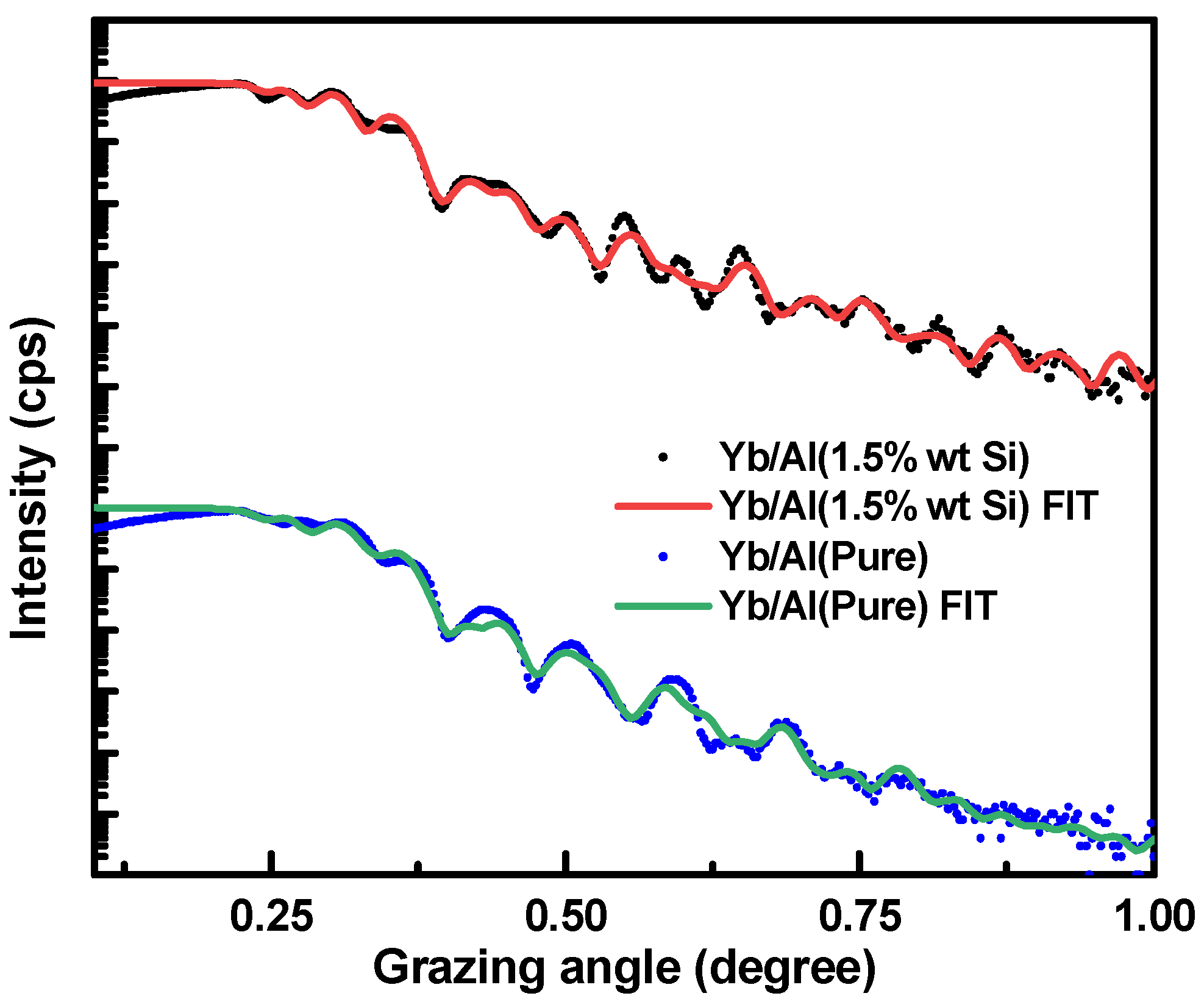
3.1. GIXRR
3.2. AFM
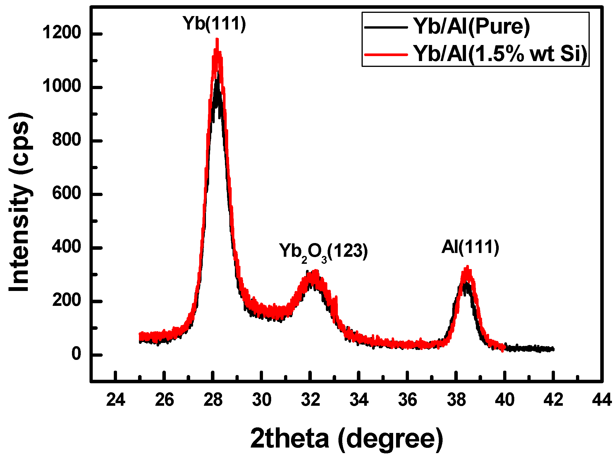
3.3. XRD
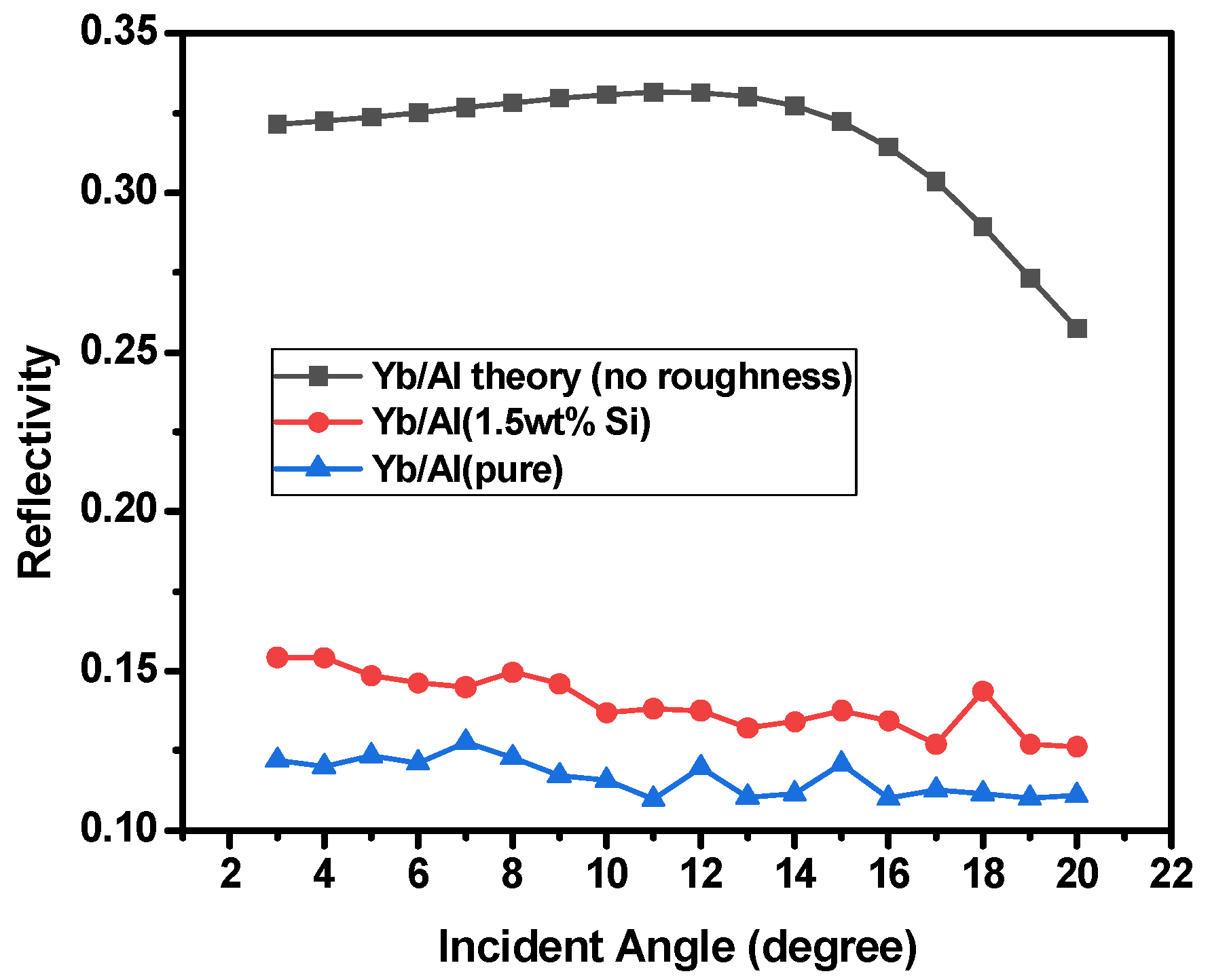
3.4. Reflectivity
4. Conclusions
Author Contributions
Funding
Institutional Review Board Statement
Informed Consent Statement
Data Availability Statement
Conflicts of Interest
References
- Corso, A.J.; Pelizzo, M.G. Extreme ultraviolet multilayers for solar physics applications: A brief review. In Proceedings Volume 11116, Astronomical Optics: Design, Manufacture, and Test of Space and Ground Systems II; SPIE: Cergy-Pontoise, France, 2019; p. 111160P. [Google Scholar]
- Domingo, V.; Fleck, B.; AI Poland. SOHO: The solar and heliosphereic observatory. Space Sci. Rev. 1995, 72, 81–84. [Google Scholar] [CrossRef]
- Kaiser, M.L.; Kucera, T.; Davila, J.M. The stereo mission: An introduction. Space Sci. Rev. 2008, 136, 5–16. [Google Scholar] [CrossRef]
- Pesnell, W.D.; Thompson, B.J.; Chamberlin, P.C. The Solar Dynamics Observatory (SDO); Springer: New York, NY, USA, 2011; pp. 3–15. [Google Scholar]
- Marsch, E.; Marsden, R.; Harrison, R. Solar Orbiter-mission profile, main goal sand present status. Adv. Space Res. 2005, 36, 1360–1366. [Google Scholar] [CrossRef]
- Zuki, C.M.; Torr, D.G. Multiple reflectors as narrow-band and broad band vacuum ultraviolet filters. Appl. Opt. 1992, 31, 1588–1596. [Google Scholar] [CrossRef] [PubMed]
- Zuki, C.M.; Torr, D.G.; Kim, J. Filters for the international solar terrestrial physics mission far-ultraviolet imager. Opt. Eng. 1993, 32, 3069–3074. [Google Scholar] [CrossRef]
- Gatto, A.; Thielsch, R.; Heber, J.; Kaiser, N.; Ristau, D.; Günster, S.; Kohlhaas, J.; Marsi, M.; Trovò, M.; Walker, R.; et al. High-performance deep-ultraviolet optics for free-electron lasers. Appl. Opt. 2002, 41, 3236–3241. [Google Scholar] [CrossRef] [PubMed]
- Uspenskii, Y.A.; Levashov, V.E.; Vinogradov, A.V.; Fedorenko, A.I.; Kondratenko, V.V.; Pershin, Y.P.; Zubarev, E.N.; Fedotov, V.Y. High-reflectivity multilayer mirrors for a vacuum ultraviolet interval of 35–50 nm. Opt. Lett. 1998, 23, 771–773. [Google Scholar] [CrossRef] [PubMed]
- Yu, L.S.; Schaefer, S.F.; Feigl, T. Enhanced reflectivity and stability of Sc/Si multilayers. In Proceedings Volume 5193, Advances in Mirror Technology for X-ray, EUV Lithography, Laser, and Other Applications; SPIE: Cergy-Pontoise, France, 2004; pp. 155–163. [Google Scholar]
- Gautier, J.; Delmotte, F.; Bridou, F. Characterization and optimization of magnetron sputtered Sc/Si Multilayers for Extreme Ultraviolet Optics. Appl. Phys. A 2007, 88, 719–725. [Google Scholar] [CrossRef]
- Takenaka, H.; Ichimaru, S.; Ohchi, T. Soft-X-ray reflectivity and heat resistance of SiC/Mg multilayer. J. Electron Spectrosc. Relat. Phenom. 2005, 144, 1047–1049. [Google Scholar] [CrossRef]
- Martínez-Galarce, D.S.; Boerner, P.; Soufli, R.; De Pontieu, B.; Katz, N.; Gullikson, E.M.; Robinson, J.C.; Baker, S.L. The high-resolution lightweight telescope for the EUV(HiLiTE). In Proceedings Volume 7011, Space Telescopes and Instrumentation 2008: Ultraviolet to Gamma Ray; SPIE: Cergy-Pontoise, France, 2008; p. 70113K. [Google Scholar]
- Windt, D.L.; Seely, J.F.; Kjornrattanawanich, B.; Uspenskii, Y.A. Terbium-based extreme ultraviolet multilayers. Opt. Lett. 2005, 30, 3186–3188. [Google Scholar] [CrossRef]
- Kjornrattanawanich, B.; Windt, D.L.; Seely, J.F.; Uspenskii, Y.A. SiC/Tb and Si/Tb multilayer coatings for extreme ultraviolet solar imaging. Appl. Opt. 2006, 45, 1765–1772. [Google Scholar] [CrossRef] [PubMed]
- Kjornrattanawanich, B.; Windt, D.L.; Seely, J.F. Normal-incidence silicon–gadolinium multilayers for imaging at 63nm wavelength. Opt. Lett. 2008, 33, 965–967. [Google Scholar] [CrossRef] [PubMed]
- Kjornrattanawanich, B.; Windt, D.L.; Uspenskii, Y.A. Optical constants determination of neodymium and gadolinium in the 3- to 100-nm wavelength range. In Proceedings Volume 6317, Advances in X-ray/EUV Optics, Components, and Applications; SPIE: Cergy-Pontoise, France, 2006; p. 63170U. [Google Scholar]
- García-Cortés, S.; Rodríguez-de Marcos, L.; Larruquert, J.I.; Aznárez, J.A.; Méndez, J.A.; Poletto, L.; Frassetto, F.; Malvezzi, A.M.; Giglia, A.; Mahne, N.; et al. Transmittance and optical constants of Lu films in the 3–1800 eV spectral range. J. Appl. Phys. 2010, 108, 063514. [Google Scholar] [CrossRef]
- Vidal-Dasilva, M.; Fernández-Perea, M.; Méndez, J.A.; Aznárez, J.A.; Larruquert, J.I. Narrow band multilayer coatings for the extreme ultraviolet range of 50–92 nm. Opt. Express 2009, 17, 22773–22784. [Google Scholar] [CrossRef] [PubMed]
- Zhong, Q.; Zhang, Z.; Ma, S.; Qi, R.Z.; Wu, J.L.; Wang, Z.S.; Jonnard, P.; Guen, L.; André, J.M. The transition from amorphous to crystalline in Al/Zr multilayers. J. Appl. Phys. 2013, 113, 133508. [Google Scholar] [CrossRef]
- Meltchakov, E. Development of Al-based multilayer optics for EUV. Appl. Phys. A 2010, 98, 111. [Google Scholar] [CrossRef]
- Meltchakov, E. EUV reflectivity and stability of tri-component Al-based multilayers. In Proceedings Volume 8168, Advances in Optical Thin Films IV; SPIE: Cergy-Pontoise, France, 2011; p. 816819. [Google Scholar]
- Meltchakov, E. Single and multi-channel Al-based multilayer systems for space applications in EUV range. In Proceedings Volume 8777, Damage to VUV, EUV, and X-ray Optics IV; and EUV and X-ray Optics: Synergy between Laboratory and Space III; SPIE: Cergy-Pontoise, France, 2013; p. 87771C. [Google Scholar]
- Delmotte, F. Development of multilayer coatings for solar orbiter EUV imaging telescopes. In Proceedings Volume 8862, Solar Physics and Space Weather Instrumentation V; SPIE: Cergy-Pontoise, France, 2013; p. 88620A. [Google Scholar]
- Wormington, M.; Panaccione, C.; Matney, K.M.; Bowen, D.K. Characterization of structures from X-ray scattering data using genetic algorithms, Philosophical Transactions of the Royal Society of London. Series A: Mathematical. Phys. Eng. Sci. 1999, 357, 2827–2848. [Google Scholar] [CrossRef]
- Uvarov, V.; Popov, I. Metrological characterization of X-ray diffraction methods for determination of crystallite size in nano-scale materials. Mater. Charact. 2007, 58, 883–891. [Google Scholar] [CrossRef]
- Feng, J.; Huang, Q.; Wang, H.; Yang, X.; Giglia, A.; Xie, C.; Wang, Z. Structure, stress and optical properties of Cr/C multilayers for the tender X-ray range. J. Synchrotron. Rad. 2019, 26, 720–728. [Google Scholar] [CrossRef]
- Yu, Y.; Ye, Z.; Jiang, L.; Yao, Q.; Li, S.; Wu, J.; Zhang, J.; Huang, Q.; Xie, C.; Sokolov, A.; et al. Laboratory-based reflectometer using line spectra of an RF-induced gas-discharge lamp in 30- to 200-nm wavelength range. J. Astron. Telesc. Instrum. Syst. 2022, 8, 017002. [Google Scholar] [CrossRef]
- Peymani, M.S.M.; Sobhani, N.A.; Rostami, M. Assessing the magnetic, cytotoxic and photocatalytic influence of incorporating Yb3+ or Pr3+ ions in cobalt–nickel ferrite. J. Mater. Sci. Mater. Electron. 2019, 30, 6902–6909. [Google Scholar] [CrossRef]
- Permin, D.A.; Novikova, A.V.; Koshkin, V.A. Fabrication and Magneto-Optical Properties of Yb2O3 Based Ceramics. Magnetochemistry 2020, 6, 63. [Google Scholar] [CrossRef]
- Kahraman, A.; Karacali, H.; Yilmaz, E. Impact and origin of the oxide-interface traps in Al/Yb2O3/n-Si/Al on the electrical characteristics. J. Alloys Compd. 2020, 825, 154171. [Google Scholar] [CrossRef]
- Hao, L.; He, G.; Fang, Z. Modulation of the microstructure, optical and electrical properties of sputtering-driven Yb2O3 gate dielectrics by sputtering power and annealing treatment. Appl. Surf. Sci. 2020, 508, 145273. [Google Scholar] [CrossRef]


| Sample | SiC Thickness | Yb Thickness | Al Thickness | Average Roughness |
|---|---|---|---|---|
| Yb/Al (pure) | 9.87 nm | 19.28 nm | 41.44 nm | 1.95 nm |
| Yb/Al (1.5 wt.% Si) | 9.68 nm | 20.57 nm | 38.78 nm | 1.89 nm |
| Sample | 10 × 10 μm2 | 4 × 4 μm2 | 1 × 1 μm2 |
|---|---|---|---|
| Yb/Al (pure) | 4.85 nm | 3.01 nm | 2.41 nm |
| Yb/Al (1.5 wt.% Si) | 1.81 nm | 2.04 nm | 2.09 nm |
| Sample | Yb (111) | Yb2O3 (123) | Al (111) |
|---|---|---|---|
| Yb/Al (pure) | 7.636 nm | 4.865 nm | 8.730 nm |
| Yb/Al (1.5 wt.% Si) | 7.895 nm | 4.915 nm | 9.318 nm |
Disclaimer/Publisher’s Note: The statements, opinions and data contained in all publications are solely those of the individual author(s) and contributor(s) and not of MDPI and/or the editor(s). MDPI and/or the editor(s) disclaim responsibility for any injury to people or property resulting from any ideas, methods, instructions or products referred to in the content. |
© 2024 by the authors. Licensee MDPI, Basel, Switzerland. This article is an open access article distributed under the terms and conditions of the Creative Commons Attribution (CC BY) license (https://creativecommons.org/licenses/by/4.0/).
Share and Cite
Lai, B.; Qi, R.; Zhang, Z.; Wang, Z. Study of Optical Performance and Structure of Yb/Al (1.5 wt.% Si) and Yb/Al (Pure) Multilayers Designed for the 73.6 nm Range. Coatings 2024, 14, 659. https://doi.org/10.3390/coatings14060659
Lai B, Qi R, Zhang Z, Wang Z. Study of Optical Performance and Structure of Yb/Al (1.5 wt.% Si) and Yb/Al (Pure) Multilayers Designed for the 73.6 nm Range. Coatings. 2024; 14(6):659. https://doi.org/10.3390/coatings14060659
Chicago/Turabian StyleLai, Bo, Runze Qi, Zengbo Zhang, and Zhanshan Wang. 2024. "Study of Optical Performance and Structure of Yb/Al (1.5 wt.% Si) and Yb/Al (Pure) Multilayers Designed for the 73.6 nm Range" Coatings 14, no. 6: 659. https://doi.org/10.3390/coatings14060659
APA StyleLai, B., Qi, R., Zhang, Z., & Wang, Z. (2024). Study of Optical Performance and Structure of Yb/Al (1.5 wt.% Si) and Yb/Al (Pure) Multilayers Designed for the 73.6 nm Range. Coatings, 14(6), 659. https://doi.org/10.3390/coatings14060659