Article

Atomic Layer Deposition Growth and Characterization of Al2O3 Layers on Cu-Supported CVD Graphene

1
Institute of Solid State Physics, Bulgarian Academy of Sciences, 72 Tzarigradsko Chaussee Blvd., 1784 Sofia, Bulgaria
2
Institute of General and Inorganic Chemistry, Bulgarian Academy of Sciences, Acad. G. Bonchev Str., Bl. 11, 1113 Sofia, Bulgaria
3
Faculty of Physics, Sofia University, 5 J. Bourchier Blvd., 1164 Sofia, Bulgaria
4
Institute of Physical Chemistry, Bulgarian Academy of Sciences, 1113 Sofia, Bulgaria
5
Department of Electrophysics, National Yang Ming Chiao Tung University, Hsinchu 30010, Taiwan
*
Author to whom correspondence should be addressed.
Coatings 2024, 14(6), 662; https://doi.org/10.3390/coatings14060662
Submission received: 29 April 2024 / Revised: 17 May 2024 / Accepted: 21 May 2024 / Published: 24 May 2024
(This article belongs to the Special Issue Application of Graphene and Two-Dimensional Materials in Thin Films)

Abstract

:
The deposition of thin uniform dielectric layers on graphene is important for its successful integration into electronic devices. We report on the atomic layer deposition (ALD) of Al2O3 nanofilms onto graphene grown by chemical vapor deposition onto copper foil. A pretreatment with deionized water (DI H2O) for graphene functionalization was carried out, and, subsequently, trimethylaluminum and DI H2O were used as precursors for the Al2O3 deposition process. The proper temperature regime for this process was adjusted by means of the ALD temperature window for Al2O3 deposition onto a Si substrate. The obtained Al2O3/graphene heterostructures were characterized by Raman and X-ray photoelectron spectroscopy, ellipsometry and atomic force and scanning electron microscopy. Samples of these heterostructures were transferred onto glass substrates by standard methods, with the Al2O3 coating serving as a protective layer during the transfer. Raman monitoring at every stage of the sample preparation and after the transfer enabled us to characterize the influence of the Al2O3 coating on the graphene film.

1. Introduction

Graphene, a single sheet of honeycomb-like arranged carbon atoms, has been in the spotlight of scientific interest for almost two decades due to its excellent physical properties [1,2,3,4,5]. This is a genuine two-dimensional material with high carrier mobility [6], extraordinary ballistic-transport distances [7] and over 97% transparency for visible light [8], which make it applicable to novel electronic and optoelectronic devices. The implementation of graphene in such integrated devices requires a technology for wafer-scale synthesis with a controllable number of layers. The experience from recent years shows that chemical vapor deposition (CVD) onto a copper catalyst is the most promising synthesis approach that yields large-area and high-quality graphene with a low density of structural defects [9]. Furthermore, this method is scalable without worsening the quality of the produced graphene [10]. Despite the problems arising from the surface morphology and the different grain orientations of the Cu foil [11,12] most commonly used as the CVD substrate/catalyst, it seems that this production technology may be able to satisfy the complex requirements for industrial applications of graphene. However, many of these applications require the graphene sheet to be coated with a conformal and ultrathin dielectric layer, which is a technological challenge due to the chemical inertness of graphene [13].
In many instances, atomic layer deposition (ALD) is the preferred technique for growing ultrathin metal oxide layers [14] as it exhibits a number of advantages, such as high-precision thickness control and excellent conformal covering of complex surfaces. However, ALD is a surface-reaction-limited process and the lack of out-of-plane functional groups in sp2-bonded graphene prevents its receptivity to an ALD reaction. For instance, combined theoretical and experimental investigations [15] showed that the adsorption of the ALD alumina precursor onto pristine graphene was kinetically and thermodynamically unfavorable, leading to nucleation, mainly at defect sites and grain boundaries, and an overall nonuniform coverage. To overcome this obstacle, various graphene pretreatment and functionalization methods have been applied [16], and intensive research has been carried out to optimize the ALD process parameters [17]. Such methods can include the chemical functionalization of graphene with NO2 and O3 [18,19], or the deposition of an additional seed [20] or interfacial protective [21] layer. Such pretreatments may have undesirable side effects, such as problems with scaling the dielectric thickness, unintentional doping or the creation of defects in the graphene lattice [22,23]. Therefore, it is important to find a way to increase the wetting of ALD dielectrics on the graphene surface without using a seed layer and without disrupting the graphene lattice. Recently, water-dipping pretreatment of graphene was suggested as such an approach [24]. According to ref. [24], the physisorbed water molecules act as nucleation sites for the metal precursor trimethylaluminum (TMA) to form continuous Al2O3 dielectric films. The use of water pretreatment as a preliminary step in the ALD process was studied in detail by Zheng et al. [25], who concluded that it generally improves Al2O3 ALD growth on graphene. The importance of physisorbed H2O molecules for the subsequent ALD Al2O3 growth was also highlighted by the results of Zhang et al. [26]. On the other hand, in ref [13], it was shown that a metal catalyst substrate of as-grown graphene can also facilitate the deposition of conformal and continuous ALD dielectric coatings. This effect was attributed to better wettability and the presence of polar sites in graphene when it is in intimate contact with its metallic substrate [13]. Recently, an improvement of graphene’s Young modulus upon deposition of an ultrathin ALD Al2O3 layer at room temperature [27] was reported.
The utilization of the outstanding electronic and optical properties of graphene includes its integration with other isolating and semiconducting layers or 3D phases, which requires refined and precise transfer procedures. Despite advancements in transfer methods for lattice disruptions, doping from contamination impurities and wrinkles are the most often occurring transfer-induced defects [28]. If deposited onto Cu-supported as-grown graphene, an ALD oxide layer could also be potentially helpful as a protective interface and support layer during the transfer process [29]. This approach avoids transfer-polymer contamination of the graphene, thus protecting it also from possible doping, which could worsen the subsequent performance of this graphene in integrated devices [29,30].
In this work, the deposition of dielectric Al2O3 thin films by ALD onto CVD-grown graphene is investigated. We deposited the Al2O3 coating with water pretreatment or directly onto the Cu-supported graphene prior to its transfer to a dielectric substrate. Besides characterization of the specimens with structural and imaging methods, we performed an on-spot Raman investigation of the graphene interaction with the Cu substrate and the impact of the ALD process.

2. Materials and Methods

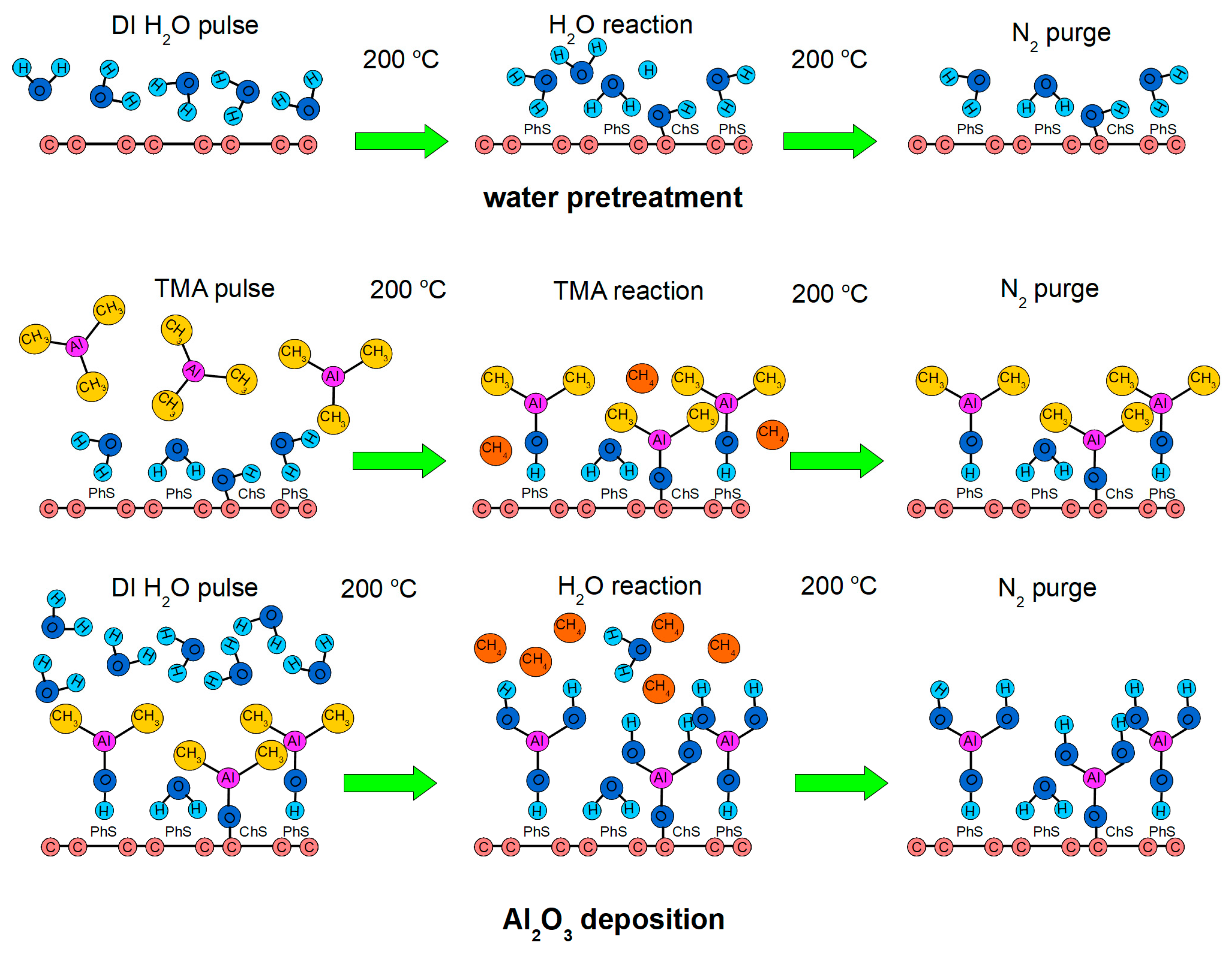
2.1. Synthesis of the Al2O3/Graphene Heterostructure

The graphene film (predominantly single-layer or double-layer graphene) was deposited onto commercially obtained copper foil (99.8%, Alfa Aesar, Haverhill, MA, USA, 25 µm thick) that was electropolished prior to the CVD process. Electropolishing was performed in 85% concentrated H3PO4 solution with the polished copper foil as the anode and a copper plate as the counter electrode at a polarization voltage of 1.98–2.02 V at room temperature. Thus, two Cu foil substrates were prepared, which will hereafter be referred to as samples S1 and S2.
The graphene was grown in a cold-wall Plasmalab System 100 research reactor from Oxford Instruments (Abingdon, Oxfordshire, UK) using low-pressure chemical vapor deposition in a high-purity hydrogen (99.9999%) and methane (99.9995%) gas flow. Prior to the growth stage, the Cu foil underwent annealing in an argon/hydrogen atmosphere at a temperature near its melting point to activate its surface catalytic properties. Subsequently, a mixture of reaction and carrier gases CH4/H2/Ar was introduced into the reaction chamber according to the corresponding recipes for single-layer graphene (applied to sample S1) and bilayer graphene (applied to sample S2). Details are given in the Supplementary Materials. Afterwards, the sample was quenched to 300 °C at 15 °C/min in a hydrogen/argon atmosphere. Cooling to room temperature was performed in a high-purity argon atmosphere. The grown graphene layers were checked by Raman spectroscopy, and representative spectra are shown in Figure S1 (Supplementary Material), indicating predominantly single-layer graphene for sample S1 and predominantly bilayer graphene for sample S2.
The deposition of Al2O3 was performed in a Beneq TFS-200 ALD system (Beneq Oy, Espoo, Finland) onto the graphene coating of the as-obtained samples S1 and S2 and an accompanying Si wafer with native oxide as the reference substrate. The ALD temperature window for the deposition of Al2O3 onto a Si substrate with TMA and deionized water (DI H2O) precursors was examined, and deposition at 200 °C was selected as the optimal thermal regime [31]. Deposition at lower temperatures leads to non-uniform, opaque and non-transparent Al2O3 films, while higher deposition temperatures create non-stoichiometric films and, particularly, increases the amount of chemisorbed oxygen [31].
The ALD process is schematically depicted in Figure 1. First, the graphene surface was pretreated in situ at 200 °C by 10 cycles of DI H2O with a 200 ms pulse duration separated by a pure nitrogen purge of 2 s. This preliminary step is needed to create hydroxyl groups (-OH) on the sp2-hybridizated graphene surface. This is assumed to be accomplished by the massive adsorption of water molecules onto the graphene surface facilitated by the Cu-induced polar traps [13]. The predominant bonding type of these water molecules is assumed to be physisorption [24], with a small amount of covalently bonded -OH groups. Estimates of the rates of these bonding types will be made in the next section.
Thereafter, a TMA and DI H2O ALD with durations of 180 ms each and separated by a 3 s nitrogen purge was performed. The nitrogen flow used as the purging and carrier gas was kept at 300 sccm during the whole deposition process. The TMA/DI H2O ALD cycle was repeated 352 times on sample S1 and 950 times on sample S2, leading to approximately 40 and 100 nm thick Al2O3 films, respectively. The growth rate of Al2O3 deposited at 200 °C with water pretreatment was estimated to be around 1.1–1.2 Å/s [31]. The thicker Al2O3 coating for sample S2 was chosen to prevent poorer ALD coverage due to the screened Cu-substrate effect upon increasing the graphene layer number [32].

2.2. Characterization

The Raman spectra were measured by backscattering geometry in the range of 100–3000 cm−1 in a HORIBA Jobin Yvon Labram HR visible spectrometer (HORIBA Scientific, Kyoto, Japan) [33] with a Peltier-cooled CCD detector and entrance slits set to 1.5 cm−1 spectral width. The 632.8 nm line of a He–Ne laser was used for the excitation using a 600 grooves/mm grating, the absolute accuracy being about 1 cm−1. The laser beam was focused on a spot of about 2 µm in diameter on the sample surface, using microscope optics with an objective of 50× magnification. The measured frequencies were calibrated using a Si standard and the line corresponding to the stretching vibrations of air nitrogen [34] at 2331 cm−1, which is contained in the spectra of Cu-supported graphene samples. In addition, the N2 line provides an internal standard for the intensity of the graphene peaks, because in the same focusing conditions, its intensity is more or less the same in all spectra of the examined Cu-supported graphene samples.
The X-ray photoelectron spectroscopy (XPS) studies were performed in a Kratos AXIS Supra spectrometer (Kratos Analytical Ltd., Manchester, UK) using achromatic AlKα radiation with an energy of 1486.6 eV. The binding energies (BEs) were determined utilizing the C 1s line with an energy of 285.0 eV as a reference. The accuracy of the measured BE was 0.1 eV. The photoelectron lines of constituent elements on the surface were recorded and corrected by subtracting a Shirley-type background and quantified using the peak area and Scofield’s photoionization cross-sections. Spectral deconvolution was performed with the XPSPEAK 4.1 software [35].
XRD measurements were performed using an Empyrean system manufactured by PANalytical, Almelo, The Netherlands. The diffractometer was configured with a Cu Ka tube, a parallel-beam mirror and a PIXcel3D detector (PANalytical, Almelo, The Netherlands). Obtained diffraction data were processed using the HighScore Plus 4.5 software and the ICSD database (Inorganic Crystal Structure Database).
The ellipsometry measurements were performed using a Woollam M2000D rotating compensator spectroscopic ellipsometer (J. A.Woollam Co. Inc., Lincoln, NE, USA) with a wavelength range from 193 nm to 1000 nm in the reflection mode. The data acquisition and analysis software involved was CompleteEASE 5.10 J. A.Woollam Co. Inc. (Lincoln, NE, USA). The spectroscopic ellipsometry data of Y and D were taken at room temperature at an angle of incidence of 60°.
The surface morphology quality was characterized by scanning electron microscopy (SEM). We used the state-of-the-art scanning electron microscope JEOL IT800SHL (Kyoto, Japan), with both in-chamber and in-lens detectors for secondary and backscattered electrons.
The microscope used for the atomic force microscopy (AFM) studies was Asylum Research’s MFP-3D Origin. The scan was run in the AC repulsion mode. The topographic images were taken on an area of 2 × 2 µm, with a line scan rate of 1Hz and a resolution of 256 × 256 points. The probes used are made of silicon (Opus-160AC-NA, OPUS by µmasch, Innovative Solutions Bulgaria Ltd., Sofia, Bulgaria), with an aluminum reflective coating and a cantilever length of 160 µm. The cantilever has a typical resonant frequency of 300 kHz, a force constant of 26 N/m, and a tip radius of 7 nm. Gwyddion 2.59 software was used for image analysis.

3. Results and Discussion

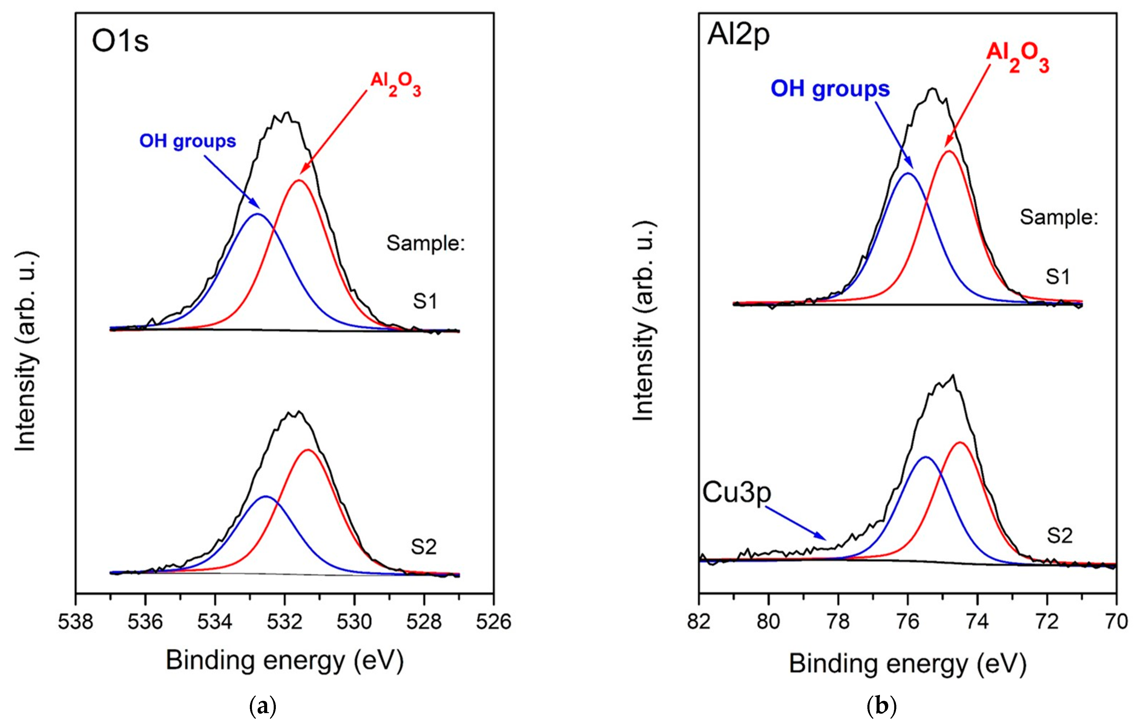
3.1. Surface Chemical Composition (XPS Analysis)

To examine the formation of the Al2O3 coating, the two samples, S1 and S2, were checked by XPS. Fitted Al2p and O1s spectral bands are displayed in Figure 2. C1s spectra were recorded; however, they do not stem from the underlying graphene film, as the XPS signal is collected from the first 10 nm beneath the surface, but from a thin surface layer of adventitious carbon instead. This C1s signal was utilized as a reference with an energy of 285.0 eV for the determination of the binding energies (BEs). From the relative intensity of the fitting components, the chemical composition of the surface region of the Al2O3 layers was also determined, and the content of the constituent elements are given in Table 1.
The O1s photoelectron spectra (Figure 2a) contain one main peak with binding energy at around 531.5 eV, typical for Al2O3, and an additional one (at 532.5 eV) appearing as a result of hydroxide and other adsorbed species on the surface of the studied samples. The Al2p photoelectron spectra (Figure 2b) are also found to have two peaks, associated with aluminum oxide and hydroxide. The main peak at around 74.5 eV is assigned to Al2O3 and the second one to adsorbed OH or other type oxygen-containing groups over the surface. Trace quantities of Cu are detected near the surface of sample S2 with the thicker Al2O3 layer. This could be due to a penetration of Cu atoms through the layer due to the occasional presence of cracks in the thicker layer. Correspondingly, in the Cu2p region, a faint peak is detected for sample S2, and a trace feature of Cu3p is also barely visible in the energy region of its Al2p band.
The binding energy separation between the O1s and Al2p core levels is 456.80 eV, in agreement with reported values for fully oxidized amorphous aluminum oxide [36,37]. Indeed, thermal ALD is known to yield amorphous Al2O3 layers for deposition temperatures up to 250 °C [38]. To verify this, we performed a structural characterization of sample S1 by X-ray diffraction, and Figure 3 presents the obtained diffraction pattern. Besides the copper substrate peak at ≈ 43° (2θ), it contains a very broad halo in the range of 13–36° (2θ) due to diffuse scattering from amorphous Al2O3. In addition, a weak signal is registered at ≈45° (2θ), which most likely arises from a trace quantity (1%–2%) of γ-Al2O3, considering the difference in intensities. The obtained spectrum in Figure 3 thus confirms the amorphous state of the Al2O3 layer, which is valid for both samples S1 and S2 due to the same growth conditions.

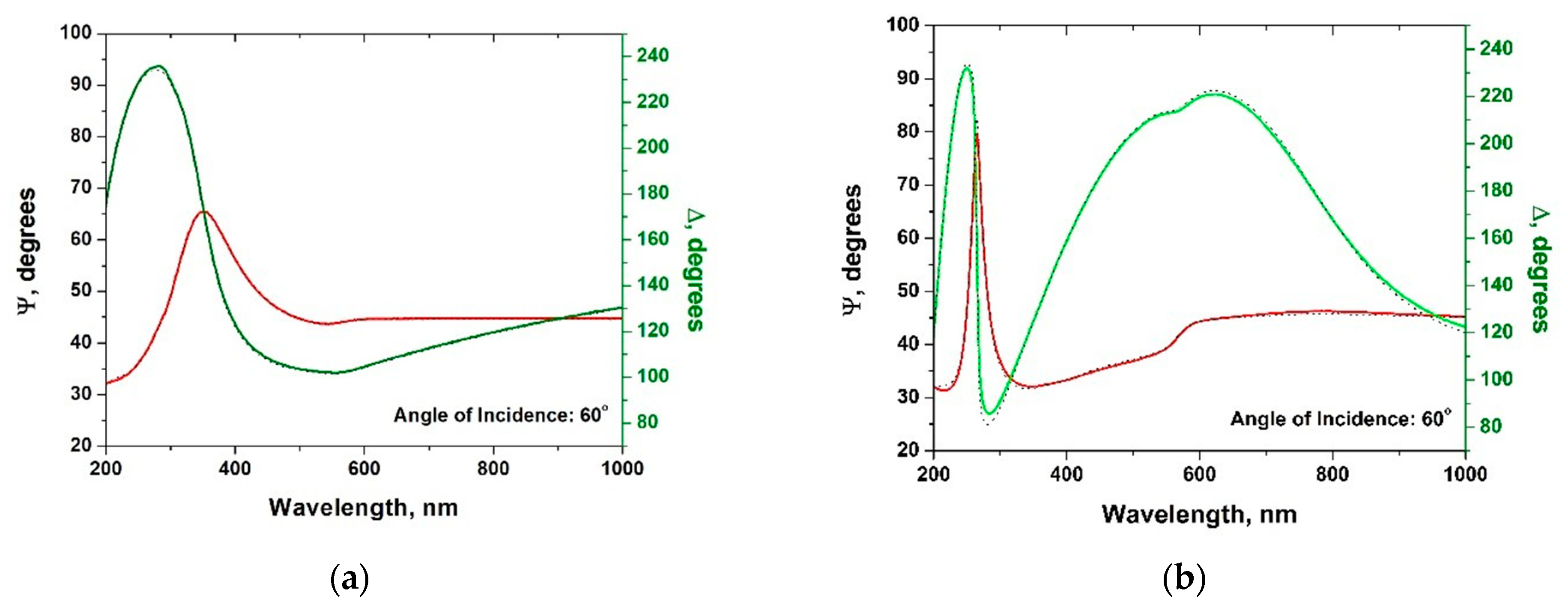
3.2. Study of the Al2O3/Graphene/Cu Heterostructures by Ellipsometry

To determine the thickness of the Al2O3 layer for the two samples, S1 and S2, spectroscopic ellipsometry (SE) measurements were carried out. The ellipsometric data for Ψ and Δ were fitted within a model consisting of three consecutive layers. The first layer is a semi-infinite oblique copper substrate, whose optical constants were determined from measurements on a freshly prepared two-component Cu/graphene system [39]. The second layer is graphene, with the optical constants of graphite taken from Palik’s Handbook of Optical Constants [40] (CompleteEASE 5.10 software). It participates in the model with two different thicknesses: 0.35 nm for sample S1 and 0.7 nm for sample S2, according to the initial Raman results for the two samples. The Al2O3 ALD layer was represented by the Cauchy dispersion. The thickness of the third component—the Al2O3 layer—was thus found to be 42 nm for sample S1 and 116 nm for sample S2. To corroborate our model, we carried out SE measurements on analogous Al2O3 layers deposited onto accompanying silicon substrates with 2.5 nm thick native oxide in the same ALD experiment. The same Al2O3 thicknesses were found, which confirms the reliability of the obtained results. The experimental Ψ and Δ data for both the 42 and 116 nm thick Al2O3 layers are presented in Figure 4a and Figure 4b, respectively. The theoretical model is represented by a dotted line.

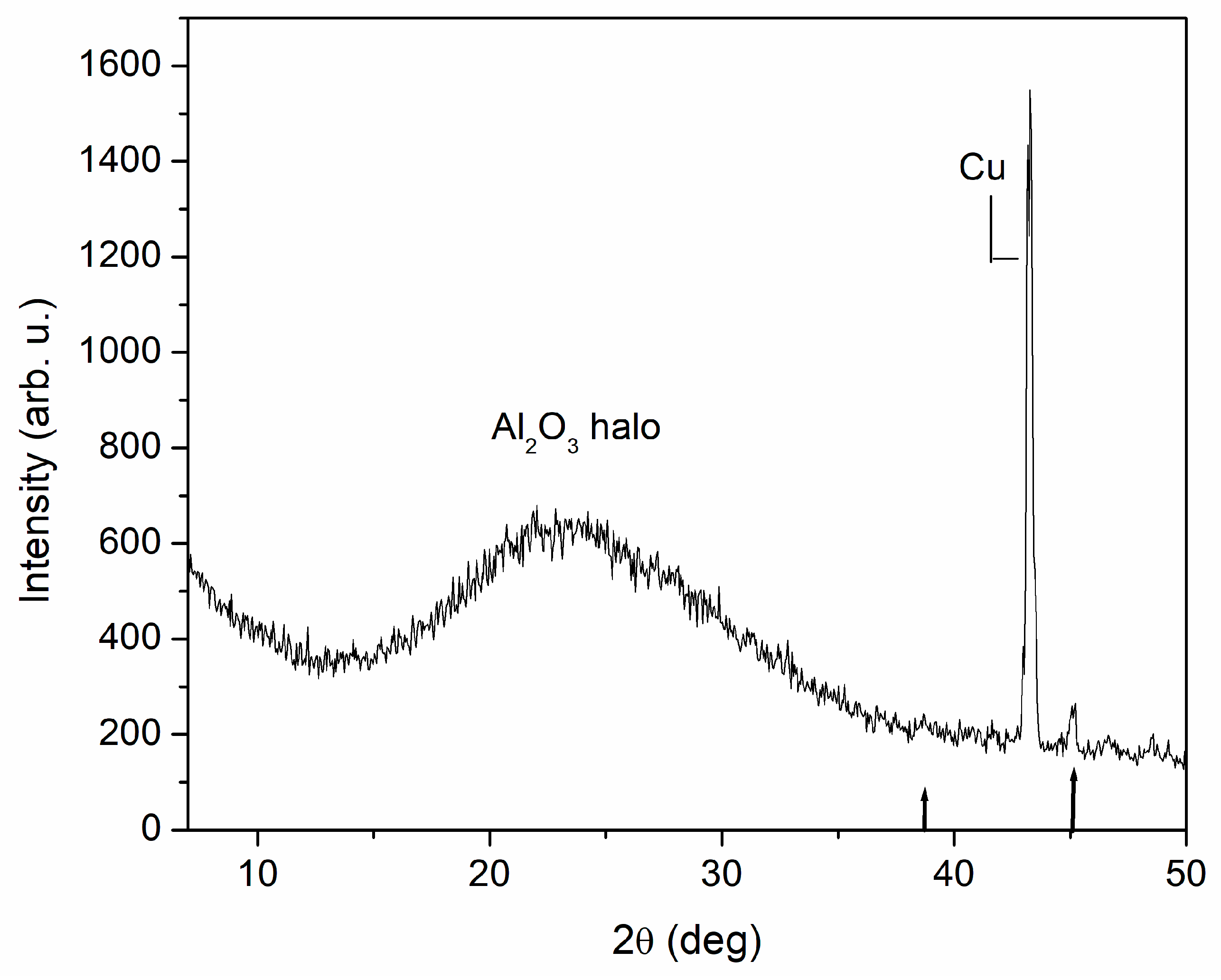
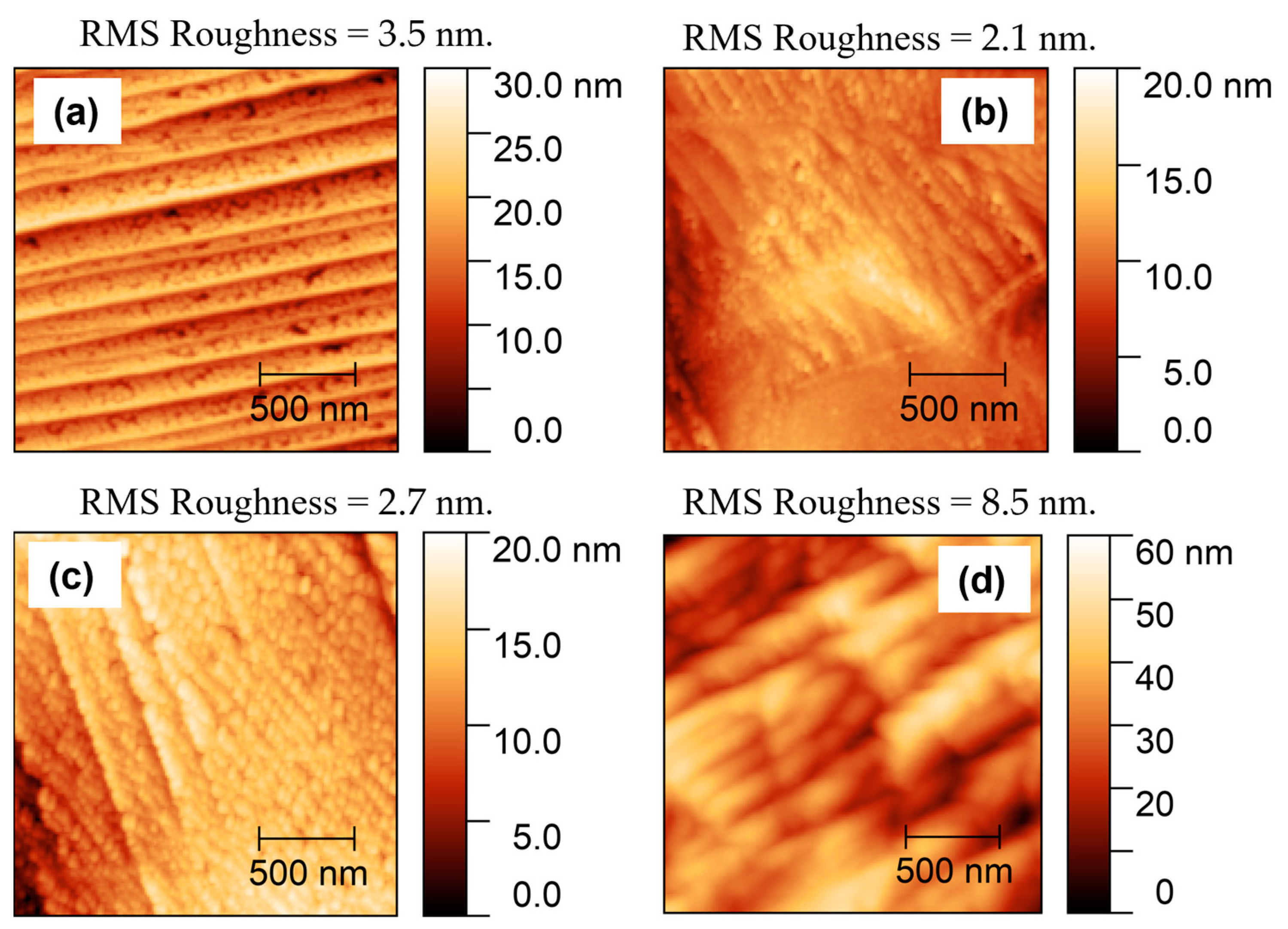
3.3. AFM and SEM Analysis
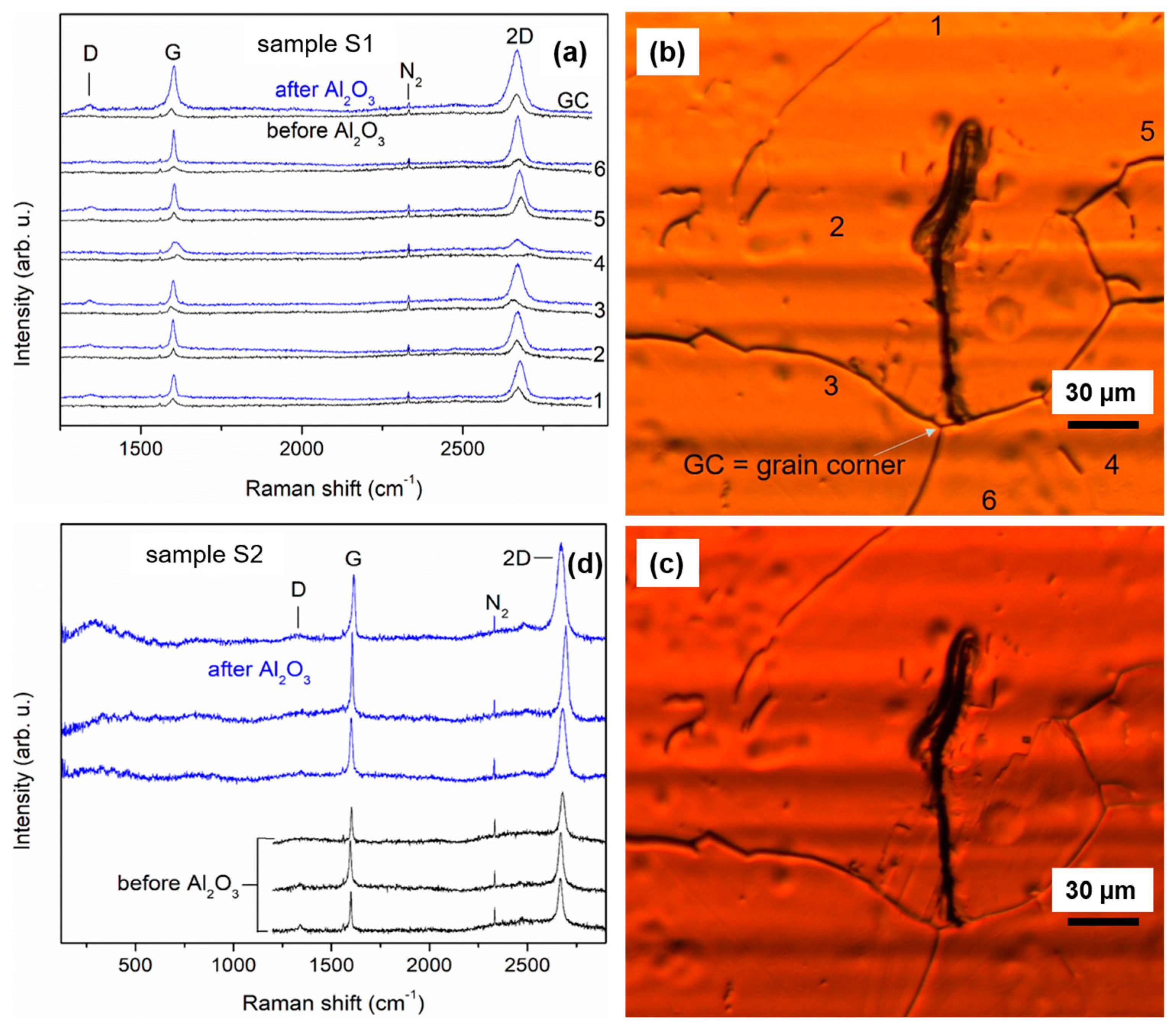
The surface morphology of the obtained Al2O3 layers was studied by AFM and SEM. AFM images of samples S1 and S2 are shown in Figure 5a–c and Figure 5d, respectively. They reveal relatively smooth Al2O3 surface for both thicknesses. Root mean square (RMS) roughness was estimated by calculating the square root of the second central moment in the data. The average RMS roughness for the three images displaying the morphology of sample S1 (Figure 5a–c) is about 2.7 nm, while for the thicker Al2O3 layer of S2 (Figure 5d), a roughness of ≈8.5 nm was found. More detailed AFM and SEM data for S2 are given in the Supplementary Materials.
SEM images from the Al2O3-coated surfaces of the studied samples are displayed in Figure 6. They show a complete and rather uniform coverage of the underlying graphene by the oxide film without pinholes, consistent with the AFM data.

3.4. Raman Analysis

Raman monitoring of both samples was carried out at every stage of the sample preparation and after the transfer. On sample S1, we encountered a region containing a characteristic defect that could be repeatedly located under an optical microscope. We were thus able to measure Raman spectra on the same selected spots with a spatial precision of about 5 μm after each processing step. Figure 7a contains such spectra measured at six smooth spots and a Cu grain boundary crossing point, which are shown in the optical micrographs in Figure 7b (before the ALD deposition) and Figure 7c (after the ALD deposition). The spectra are grouped in couples to illustrate, for each examined spot, the change in the Raman response caused by the Al2O3 ALD deposition. Figure 7d presents Raman spectra illustrating this effect for sample S2. Further details of the Raman characterization are given in the Supplementary Materials.
The spectra taken from the as-grown graphene reflect a uniform picture of strong coupling to the Cu substrate [41], manifested by suppressed Raman intensity and a strong blue shift of the G and the 2D bands (≈10 and ≈35 cm−1, respectively [39,42]). Multiple enhancement of the intensity of all Raman bands of the graphene in sample S1 is observed as an immediate consequence of the ALD process; however, the blue shift largely remains the same. The same effect is established also for sample S2; however, the ALD-induced intensity enhancement there is much weaker and only reaches, at most, 50%. We attribute these effects to the complex interplay of interactions to which graphene is subjected in the obtained sandwich structure. The intimate contact with copper creates polar traps [13], making graphene more susceptible to the adsorption of H2O and, probably, TMA molecules. The massive adsorption of such species during ALD, in turn, slightly modifies the graphene–Cu coupling but does not relax it. A further indication that the coupling is largely preserved is the lack of Cu2O-related spectral bands in the region of 100–650 cm−1 [43] in the Raman spectra measured after the ALD process (see Figure 7d and Figure S4). Because this is a 200 °C process with water pretreatment, we conclude that even the single-layer graphene in sample S1 effectively prevents the penetration of ALD-related species toward the Cu surface, in contrast to other oxide deposition processes that oxidize the substrate [44]. As can be appreciated from the relatively symmetric shape of the 2D band in the spectra of sample S2 in Figure S1 and Figure 7d, its graphene layer consists mostly of twisted bilayer graphene. In this case, the two monolayers do not strongly interact [45], and the coupling to the Cu substrate may have a weaker impact on the upper layer. This may explain the weaker Raman intensity enhancement in sample S2 after the ALD process.
Now, we discuss the possible bonding types between graphene and the adsorbed water molecules during the ALD pretreatment step. We consider the predominant bonding type to be physisorption [24], with a small amount of covalently bonded -OH groups. A covalent bond constitutes a zero-dimensional point-like defect, and the D peak provides information on such defects in the graphene lattice. The ratio of its intensity to that of the G peak, ID/IG, is typically used as measure for the defect density [46]. We found the increase in this ratio caused only by the ALD process to be in the range 0.1–0.2 for the spectra in Figure 7a. Using the defect quantification model proposed in ref. [46] and assuming that the impact of the ALD process was the creation of a certain number of covalent C-OH bonds, we estimate the average distance between two neighboring C-OH bonds to be 30–50 nm, which yields a surface density of about 103 per µm2. On the other hand, the surface density of all adsorbed H2O molecules can be assumed to be approximately equal to the surface density of Cu-induced polar traps, which, according to ref. [13], reaches 105–106 per µm2. Thus, the rate of covalent C-OH bonds can be roughly estimated to be ≈1%. However, our Raman data from aged samples presented in the Supplementary Materials (Figure S4) shows a broadening of the G peak and a sharp increase in ID/IG over larger timescales, which imply that oxidation reactions may slowly advance at the Al2O3/graphene interface over time. This raises concerns about the long-term stability of such heterostructures and, especially, the performance sustainability of devices into which they are integrated.
Parts of both samples were transferred to microscope glass slides using poly-methyl-methacrylate (PMMA)-assisted wet transfer. The presence of nanoscale Al2O3 allows for a much thinner PMMA film than typically used (about 150 nm). It further protects the graphene from PMMA contamination and facilitates subsequent removal of the backbone polymer [47]. The PMMA (2% in anisole) was spin coated at ~4000 rpm, resulting in about a 50–70 nm layer. Then, the samples were cured for 2 min at 180 °C and floated on a Fe(NO3)3•9H2O solution to etch the Cu foil. Finally, after a few cycles of rinsing in DI water, the PMMA was dissolved in acetone at 80 °C for few hours.
Raman spectra from the two transferred Al2O3/graphene heterostructures are displayed in Figure 8. The values of the 2D-to-G peak intensity ratio I(2D)/I(G) obtained from these spectra of about 1 for sample S2 and 2–3 for sample S1 confirm that they represent bi- and monolayer graphene, respectively (see also Figure S1). For both transferred heterostructures, we found typical ID/IG values in the range between 0.05 and 0.1, indicating that the ALD process used for Al2O3 growth does not damage the underlying graphene. The full width at half-maximum (FWHM) of the 2D peak was found to be in the range of 30–35 cm−1 for sample S1 and 35–38 cm−1 for S2, which is only insignificantly higher than the typical values for CVD graphene. The FWHM of the 2D peak is informative for the local strain variations in the graphene layer [48]. Furthermore, after transfer, the G and 2D peak frequencies are around 1588 and 2650 cm−1, respectively, thus exhibiting a slight residual blue shift, especially for the single-layer graphene sample. We attribute this blue shift to a compressive strain imposed by the oxide layer [20], which, on the other hand, indicates a strong and reliable adhesion of the Al2O3 layer on the underlying graphene. The spectra are almost free of Raman signals from transfer residues, especially those stemming from sample S1 with the thinner and smoother Al2O3 layer, thus confirming its protecting function during the transfer. Such a layer of 30–40 nm thickness, which is still relatively smooth and crack-free, according to the XPS results, seems to be optimal for wet-chemistry transfer.
In summary, we performed ALD Al2O3 deposition with water pretreatment on as-grown Cu-supported CVD graphene. After characterization of the specimens by structural and imaging methods, we carried out a detailed on-spot Raman investigation of the graphene interaction with the Cu substrate, the impact of the ALD process and the post-ALD time evolution of the Al2O3/graphene/Cu system. Our results indicate possible problems in the practical use of Al2O3/graphene heterostructures prepared by ALD with water pretreatment.

4. Conclusions

We prepared Al2O3/graphene heterostructures by the chemical vapor deposition of graphene onto copper foil and subsequent atomic layer deposition of Al2O3 onto the Cu-supported graphene. Characterization of the obtained heterostructures by X-ray photoelectron spectroscopy, ellipsometry and atomic force and scanning electron microscopy revealed smooth Al2O3 coatings with complete coverage and controllable thickness. Samples of these heterostructures were transferred onto glass substrates by standard methods, with the Al2O3 coating serving as a protective layer during the transfer. On-spot Raman monitoring at every stage of the sample preparation and after the transfer confirmed that graphene endures the Al2O3 ALD growth without significant defect formation and effectively prevents the penetration of ALD-related species toward the Cu-substrate surface. However, our results indicate that after ALD Al2O3 deposition with water pretreatment, oxidation reactions may slowly advance at the Al2O3/graphene interface with time. Therefore, special care should be taken to block these reactions when integrating such heterostructures into electronic devices.

Supplementary Materials

The following supporting information can be downloaded at: https://www.mdpi.com/article/10.3390/coatings14060662/s1, Details of CVD graphene growth process parameters; Raman check and estimation of the thickness of the CVD grown graphene samples; additional AFM and SEM results for Sample S2; study of the effects of aging of the Al2O3/graphene heterostructure.

Author Contributions

Conceptualization: P.R. and V.M.; methodology: P.S., V.M. and B.B.; validation: P.R., B.B., I.A., P.T., K.K. and G.A.; formal analysis: P.S. and S.P.; investigation: P.R., I.A., P.T., K.K., B.R., G.A. and S.P.; writing—original draft preparation: P.R.; writing—review and editing: P.R, I.A., B.R. and S.H.L.; visualization: K.K., B.R. and S.P.; supervision: P.R. and S.H.L.; project administration: P.R.; funding acquisition: P.R. All authors have read and agreed to the published version of the manuscript.

Funding

This research was funded by The Bulgarian National Science Fund, grant number KP-06-N38/10 from 06.12.2019. B.R. acknowledges the support from Project INFRAMAT—part of the Bulgarian National Roadmap for Scientific Infrastructure, supported by the Ministry of Education and Science. K.K. acknowledges the support from the European Regional Development Fund within the Operational Programme “Science and Education for Smart Growth 2014–2020” under the Project CoE “National center of mechatronics and clean technologies “BG05M2OP001-1.001-0008”. S.H.L. and S.P. acknowledge funding by the National Science and Technology Council of Taiwan, grant number NSTC 112-2811-E-A49-540.

Institutional Review Board Statement

Not applicable.

Informed Consent Statement

Not applicable.

Data Availability Statement

The data presented in this study are available from the corresponding author upon reasonable request.

Conflicts of Interest

The authors declare no conflicts of interest. The funders had no role in the design of the study; in the collection, analyses, or interpretation of the data; in the writing of the manuscript; or in the decision to publish the results.

References

  1. Novoselov, K.S.; Geim, A.K.; Morozov, S.V.; Jiang, D.; Zhang, Y.; Dubonos, S.V.; Grigorieva, I.V.; Firsov, A.A. Electric field effect in atomically thin carbon films. Science 2004, 306, 666. [Google Scholar] [CrossRef]
  2. Novoselov, K.S.; Geim, A.K.; Morozov, S.V.; Jiang, D.; Katsnelson, M.I.; Grigorieva, I.V.; Dubonos, S.V.; Firsov, A.A. Two-dimensional gas of massless Dirac fermions in graphene. Nature 2005, 438, 197. [Google Scholar] [CrossRef]
  3. Zhang, Y.; Tan, Y.W.; Stormer, H.L.; Kim, P. Experimental observation of the quantum Hall effect and Berry’s phase in graphene. Nature 2005, 438, 201. [Google Scholar] [CrossRef]
  4. Balandin, A.A.; Ghosh, S.; Bao, W.; Calizo, I.; Teweldebrhan, D.; Miao, F.; Lau, C.N. Superior thermal conductivity of single-layer graphene. Nano Lett. 2008, 8, 902. [Google Scholar] [CrossRef]
  5. Lee, C.; Wei, X.; Kysar, J.W.; Hone, J. Measurement of the elastic properties and intrinsic strength of monolayer graphene. Science 2008, 321, 385. [Google Scholar] [CrossRef]
  6. Chen, J.-H.; Jang, C.; Xiao, S.; Ishigami, M.; Fuhrer, M.S. Intrinsic and extrinsic performance limits of graphene devices on SiO2. Nat. Nanotechnol. 2008, 3, 206. [Google Scholar] [CrossRef]
  7. Du, X.; Skachko, I.; Barker, A.; Andrei, E.Y. Approaching ballistic transport in suspended graphene. Nat. Nanotechnol. 2008, 3, 491. [Google Scholar] [CrossRef]
  8. Nair, R.R.; Blake, P.; Grigorenko, A.N.; Novoselov, K.S.; Booth, T.J.; Stauber, T.; Peres, N.M.R.; Geim, A.K. Fine structure constant defines visual transparency of graphene. Science 2008, 320, 1308. [Google Scholar] [CrossRef]
  9. Li, X.; Cai, W.; An, J.; Kim, S.; Nah, J.; Yang, D.; Piner, R.; Velamakanni, A.; Jung, I.; Tutuc, E.; et al. Large-area synthesis of high-quality and uniform graphene films on copper foils. Science 2009, 324, 1312–1314. [Google Scholar] [CrossRef]
  10. Bae, S.; Kim, H.; Lee, Y.; Xu, X.; Park, J.-S.; Zheng, Y.; Balakrishnan, J.; Lei, T.; Ri Kim, H.; Song, Y.I.; et al. Roll-to-roll production of 30-inch graphene films for transparent electrodes. Nat. Nanotechnol. 2010, 5, 574–578. [Google Scholar] [CrossRef]
  11. Han, G.H.; Güneş, F.; Bae, J.J.; Kim, E.S.; Chae, S.J.; Shin, H.-J.; Choi, J.-Y.; Pribat, D.; Lee, Y.H. Influence of copper morphology in forming nucleation seeds for graphene growth. Nano Lett. 2011, 11, 4144–4148. [Google Scholar] [CrossRef]
  12. Wood, J.D.; Schmucker, S.W.; Lyons, A.S.; Pop, E.; Lyding, J.W. Effects of polycrystalline Cu substrate on graphene growth by chemical vapor deposition. Nano Lett. 2011, 11, 4547. [Google Scholar]
  13. Dlubak, B.; Kidambi, P.R.; Weatherup, R.S.; Hofmann, S.; Robertson, J. Substrate-assisted Nucleation of Ultra-thin Dielectric Layers on Graphene by Atomic Layer Deposition. Appl. Phys. Lett. 2012, 100, 173113. [Google Scholar] [CrossRef]
  14. Puurunen, R.L. Surface chemistry of atomic layer deposition: A case study for the trimethylaluminum/water process. J. Appl. Phys. 2005, 97, 121301. [Google Scholar]
  15. Vervuurt, R.H.J.; Karasulu, B.; Verheijen, M.A.; Kessels, W.M.M.; Bol, A.A. Uniform Atomic Layer Deposition of Al2O3 on Graphene by Reversible Hydrogen Plasma Functionalization. Chem. Mater. 2017, 29, 2090–2100. [Google Scholar] [CrossRef] [PubMed]
  16. Zhou, Y.; Wang, J.; He, P.; Chen, S.; Chen, Z.; Zang, Y.; Li, Y.; Duan, Y. ALD-Assisted Graphene Functionalization for Advanced Applications. J. Electron. Mater. 2022, 51, 2766–2785. [Google Scholar] [CrossRef]
  17. Aria, A.I.; Nakanishi, K.; Xiao, L.; Braeuninger-Weimer, P.; Sagade, A.A.; Alexander-Webber, J.A.; Hofmann, S. Parameter Space of Atomic Layer Deposition of Ultrathin Oxides on Graphene. ACS Appl. Mater. Interfaces 2016, 8, 30564. [Google Scholar] [CrossRef] [PubMed]
  18. Young, M.J.; Musgrave, C.B.; George, S.M. Growth and Characterization of Al2O3 Atomic Layer Deposition Films on sp2-Graphitic Carbon Substrates Using NO2/Trimethylaluminum Pretreatment. ACS Appl. Mater. Interfaces 2015, 7, 12030–12037. [Google Scholar] [CrossRef] [PubMed]
  19. Jandhyala, S.; Mordi, G.; Lee, B.; Lee, G.; Floresca, C.; Cha, P.R.; Ahn, J.; Wal-lace, R.M.; Chabal, Y.J.; Kim, M.J.; et al. Atomic Layer Deposition of Dielectrics on Graphene Using Reversibly Physisorbed Ozone. ACS Nano 2012, 6, 2722. [Google Scholar] [CrossRef]
  20. Robinson, J.A.; LaBella, M.; Trumbull, K.A.; Weng, X.; Cavelero, R.; Daniels, T.; Hughes, Z.; Hollander, M.; Fanton, M.; Snyder, D. Epitaxial Graphene Materials Integration: Effects of Dielectric Overlayers on Structural and Electronic Properties. ACS Nano 2010, 4, 2667–2672. [Google Scholar] [CrossRef]
  21. Canto, B.; Otto, M.; Powell, M.J.; Babenko, V.; O’Mahony, A.; Knoops, H.C.M.; Sundaram, R.S.; Hofmann, S.; Lemme, M.C.; Neumaier, D. Plasma-Enhanced Atomic Layer Deposition of Al2O3 on Graphene Using Monolayer hBN as Interfacial Layer. Adv. Mater. Technol. 2021, 6, 2100489. [Google Scholar] [CrossRef]
  22. Nayfeh, O.M.; Marr, T.; Dubey, M. Impact of plasma-assisted atomic-layer-deposited gate dielectric on graphene transistors. IEEE Electron Device Lett. 2011, 32, 473. [Google Scholar] [CrossRef]
  23. Liu, L.; Ryu, S.; Tomasik, M.R.; Stolyarova, E.; Jung, N.; Hybertsen, M.S.; Steigerwald, M.L.; Brus, L.E.; Flynn, G.W. Graphene oxidation: Thickness-dependent etching and strong chemical doping. Nano Lett. 2008, 8, 1965. [Google Scholar] [CrossRef]
  24. Cao, Y.-Q.; Cao, Z.-Y.; Li, X.; Wu, D.; Li, A.-D. A facile way to deposit conformal Al2O3 thin film on pristine graphene by atomic layer deposition. Appl. Surf. Sci. 2014, 291, 78–82. [Google Scholar] [CrossRef]
  25. Zheng, L.; Cheng, X.; Cao, D.; Wang, G.; Wang, Z.; Xu, D.; Xia, C.; Shen, L.; Yu, Y.; Shen, D. Improvement of Al2O3 Films on Graphene Grown by Atomic Layer Deposition with Pre-H2O Treatment. Appl. Mater. Interfaces 2014, 6, 7014–7019. [Google Scholar] [CrossRef]
  26. Zhang, Y.; Qiu, Z.; Cheng, X.; Xie, H.; Wang, H.; Xie, X.; Yu, Y.; Liu, R. Direct Growth of High-Quality Al2O3 Dielectric on Graphene Layers by Low-Temperature H2O-Based ALD. J. Phys. D Appl. Phys. 2014, 47, 055106. [Google Scholar] [CrossRef]
  27. Tamm, A.; Kahro, T.; Piirsoo, H.-M.; Jõgiaas, T. Atomic-Layer-Deposition-Made Very Thin Layer of Al2O3 Improves the Young’s Modulus of Graphene. Appl. Sci. 2022, 12, 2491. [Google Scholar] [CrossRef]
  28. Song, Y.; Zou, W.; Lu, Q.; Lin, L.; Liu, Z. Graphene Transfer: Paving the Road for Applications of Chemical Vapor Deposition Graphene. Small 2021, 17, 2007600. [Google Scholar] [CrossRef]
  29. Cabrero-Vilatela, A.; Alexander-Webber, J.A.; Sagade, A.A.; Aria, A.I.; Braeuninger-Weimer, P.; Martin, M.; Weatherup, R.S.; Hofmann, S. Atomic layer deposited oxide films as protective interface layers for integrated graphene transfer. Nanotechnology 2017, 28, 485201. [Google Scholar] [CrossRef]
  30. Shivayogimath, A.; Eriksson, L.; Whelan, P.R.; Mackenzie, D.M.A.; Luo, B.; Bøggild, P.; Booth, T.J. Atomic Layer Deposition Alumina-Mediated Graphene Transfer for Reduced Process Contamination. Phys. Status Solidi RRL 2019, 13, 1900424. [Google Scholar] [CrossRef]
  31. Blagoev, B.S.; Delibatov, D.A.; Mehandzhiev, V.B.; Sveshtarov, P.; Terziyska, P.; Avramova, I.; Rafailov, P.M. Optimization of atomic layer deposition of Al2O3 films as possible template for graphene transfer. J. Phys. Conf. Ser. 2022, 2240, 012002. [Google Scholar] [CrossRef]
  32. Schilirò, E.; Lo Nigro, R.; Roccaforte, F.; Giannazzo, F. Substrate-Driven Atomic Layer Deposition of High-k Dielectrics on 2D Materials. Appl. Sci. 2021, 11, 11052. [Google Scholar] [CrossRef]
  33. Cazzanelli, E.; De Luca, O.; Vuono, D.; Policicchio, A.; Castriota, M.; Desiderio, G.; De Santo, M.P.; Aloise, A.; Fasanella, A.; Rugiero, T.; et al. Characterization of graphene grown on copper foil by chemical vapor deposition (CVD) at ambient pressure conditions. J. Raman Spectrosc. 2018, 49, 1006–1014. [Google Scholar] [CrossRef]
  34. Horiba Scientific. Available online: https://www.horiba.com/int/scientific/technologies/raman-imaging-and-spectroscopy (accessed on 10 May 2024).
  35. XPSPEAK41 Version 4.1 Is Free, Fully Featured, Software for the Analysis of XPS Spectra. Available online: https://xpspeak.software.informer.com (accessed on 14 November 2023).
  36. Renault, O.; Gosset, L.G.; Rouchon, D.; Ermolieff, A. Angle-resolved X-ray Photoelectron Spectroscopy of Ultrathin Al2O3 Films Grown by Atomic Layer Deposition. J. Vac. Sci. Technol. A 2002, 20, 1867–1876. [Google Scholar] [CrossRef]
  37. van den Brand, J.; Snijders, P.C.; Sloof, W.G.; Terryn, H.; de Wit, J.H.W. Acid-base Characterization of Aluminum Oxide Surfaces with XPS. J. Phys. Chem. B 2004, 108, 6017–6024. [Google Scholar] [CrossRef]
  38. Barbosa, C.; Blanc-Pelissiera, D.; Favea, A.; Blanquetb, E.; Criscib, A.; Fourmonda, E.; Albertinia, D.; Sabaca, A.; Ayadia, K.; Girarda, P.; et al. Characterization of Al2O3 thin films prepared by thermal ALD. Energy Procedia 2015, 77, 558–564. [Google Scholar] [CrossRef]
  39. Rafailov, P.M.; Sveshtarov, P.K.; Mehandzhiev, V.B.; Avramova, I.; Terziyska, P.; Petrov, M.; Katranchev, B.; Naradikian, H.; Boyadjiev, S.; Cserháti, C.; et al. Growth and Characterization of Graphene Layers on Different Kinds of Copper Surfaces. Molecules 2022, 27, 1789. [Google Scholar] [CrossRef]
  40. Palik, E. Handbook of Optical Constants of Solids, 1st ed.; Evsevier: Amsterdam, The Netherlands, 1997. [Google Scholar]
  41. Wu, R.; Gan, L.; Ou, X.; Zhang, Q.; Luo, Z. Detaching graphene from copper substrate by oxidation-assisted water intercalation. Carbon 2016, 98, 138. [Google Scholar] [CrossRef]
  42. Choi, J.; Koo, S.; Song, M.; Jung, D.; Choi, S.; Ryu, S. Varying electronic coupling at graphene-copper interfaces probed with Raman spectroscopy. 2D Mater. 2020, 7, 025006. [Google Scholar] [CrossRef]
  43. Debbichi, L.; de Lucas, M.C.M.; Pierson, J.F.; Krüger, P. Vibrational Properties of CuO and Cu4O3 from First-Principles Calculations, and Raman and Infrared Spectroscopy. J. Phys. Chem. C 2012, 116, 10232–10237. [Google Scholar] [CrossRef]
  44. Morales, C.; Urbanos, F.J.; del Campo, A.; Leinen, D.; Granados, D.; Rodríguez, M.A.; Soriano, L. Electronic Decoupling of Graphene from Copper Induced by Deposition of ZnO: A Complex Substrate/Graphene/Deposit/Environment Interaction. Adv. Mater. Interfaces 2020, 7, 1902062. [Google Scholar] [CrossRef]
  45. Poncharal, P.; Ayari, A.; Michel, T.; Sauvajol, J.-L. Raman spectra of misoriented bilayer graphene. Phys. Rev. B 2008, 78, 113407. [Google Scholar] [CrossRef]
  46. Cançado, L.G.; Jorio, A.; Ferreira, E.H.M.; Stavale, F.; Achete, C.A.; Capaz, R.B.; Moutinho, M.V.O.; Lombardo, A.; Kulmala, T.S.; Ferrari, A.C. Quantifying Defects in Graphene via Raman Spectroscopy at Different Excitation Energies. Nano Lett. 2011, 11, 3190–3196. [Google Scholar] [CrossRef] [PubMed]
  47. Grebel, H.; Stan, L.; Sumant, A.V.; Liu, Y.; Gosztola, D.; Ocola, L.; Fisher, B. Transfer of Graphene with Protective Oxide Layers. ChemEngineering 2018, 2, 58. [Google Scholar] [CrossRef]
  48. Neumann, C.; Reichardt, S.; Venezuela, P.; Drögeler, M.; Banszerus, L.; Schmitz, M.; Watanabe, K.; Taniguchi, T.; Mauri, F.; Beschoten, B.; et al. Raman spectroscopy as probe of nanometre-scale strain variations in graphene. Nat. Commun. 2015, 6, 8429. [Google Scholar] [CrossRef]
Figure 1. Schematic representation of the ALD Al2O3 growth process: the water pretreatment step and two half-reactions of the main TMA transformation cycle triggered by the TMA pulse and the DI H2O pulse, respectively.
Coatings 14 00662 g001
Figure 2. Detailed XPS spectra depicting the surface state of samples S1 and S2 in the O1s (a) and Al2p (b) regions.
Coatings 14 00662 g002
Figure 3. X-ray diffraction spectrum of sample S1. The two vertical arrows mark the 2θ values at which the γ-Al2O3 peaks (111) and (002) normally appear.
Coatings 14 00662 g003
Figure 4. Ψ and Δ spectra (red and green lines respectively) acquired for (a) sample S1 with 42 nm thick Al2O3 and (b) sample S2 with 116 nm thick Al2O3. Dotted lines represent the theoretical model.
Coatings 14 00662 g004
Figure 5. AFM images of sample S1 with 42 nm Al2O3 (ac) and S2 with 116 nm Al2O3 (d).
Coatings 14 00662 g005
Figure 6. SEM images of samples S1 with 42 nm Al2O3 (a) and S2 with 116 nm Al2O3 (b). The scale bars represent 500 nm.
Coatings 14 00662 g006
Figure 7. (a) Raman spectra of sample S1 from the spots marked with consecutive numbers and the symbol “GC” in the optical micrograph (b) to the left. The spectra are grouped in couples marked correspondingly, with the upper spectrum (blue) taken before the ALD Al2O3 growth and lower spectrum (black) taken after that process. (b) Optical micrograph of a region of sample S1 with a characteristic defect right after the CVD graphene growth. (c) Optical micrograph of the same region right after the ALD Al2O3 growth. (d) Representative Raman spectra of sample S2 measured before (black) and after (blue) the ALD Al2O3 growth.
Coatings 14 00662 g007
Figure 8. Representative Raman spectra from the two Al2O3/graphene heterostructures resulting from samples S1 and S2 after their transfer onto a glass substrate.
Coatings 14 00662 g008
Table 1. Chemical composition at the surface of the two Al2O3/graphene/Cu samples.
SampleC, at. %O, at. %Cu, at. %Al, at. %Al/O Ratio
S115.449.0-35.60.7
S229.840.50.429.30.7
Disclaimer/Publisher’s Note: The statements, opinions and data contained in all publications are solely those of the individual author(s) and contributor(s) and not of MDPI and/or the editor(s). MDPI and/or the editor(s) disclaim responsibility for any injury to people or property resulting from any ideas, methods, instructions or products referred to in the content.

