Article

Identification of Elastoplastic Constitutive Model of GaN Thin Films Using Instrumented Nanoindentation and Machine Learning Technique

1
CEMMPRE, Department of Mechanical Engineering, University of Coimbra, Rua Luís Reis Santos, 3030-788 Coimbra, Portugal
2
Laboratoire de Génie Mécanique, École Nationale d’Ingénieurs de Monastir, Université de Monastir, Av. Ibn El-Jazzar, Monastir 5019, Tunisia
3
DGM, Institut Supérieur des Sciences Appliquées et de Technologie de Sousse, Université de Sousse, Cité Ibn Khaldoun, Sousse 4003, Tunisia
4
Departamento de Engenharia Informática, Faculdade de Ciências e Tecnologia, Universidade de Coimbra, Pólo II—Pinhal de Marrocos, 3030-290 Coimbra, Portugal
5
Laboratory of Multifunctional Materials and Applications (LaMMA), Department of Physics, Faculty of Sciences of Sfax, University of Sfax, Soukra Road km 3.5, B.P. 1171, Sfax 3000, Tunisia
*
Author to whom correspondence should be addressed.
Coatings 2024, 14(6), 683; https://doi.org/10.3390/coatings14060683
Submission received: 9 May 2024 / Revised: 28 May 2024 / Accepted: 28 May 2024 / Published: 31 May 2024
(This article belongs to the Special Issue Recent Advances in the Development of Thin Films)

Abstract

:
This study presents a novel inverse identification approach to determine the elastoplastic parameters of a 2 µm thick GaN semiconductor thin film deposited on a sapphire substrate. This approach combines instrumented nanoindentation with finite element (FE) simulations and an artificial neural network (ANN) model. Experimental load–depth curves were obtained using a Berkovich indenter. To generate a comprehensive database for the inverse analysis, FE models were constructed to simulate load–depth responses across a wide range of GaN thin film properties. The accuracy of both 2D and 3D simulations was compared to select the optimal model for database generation. The Box–Behnken design-based data sampling method was used to define the number of simulations and input variables for the FE models. The ANN technique was then employed to establish the complex mapping between the simulated load–depth curves (input) and the corresponding stress–strain curve (output). The generated database was used to train and test the ANN model. Then, the learned ANN model was used to achieve high accuracy in identifying the stress–strain curve of the GaN thin film from the experimental load–depth data. This work demonstrates the successful application of an inverse analysis framework, combining experimental nanoindentation tests, FE modeling, and an ANN model, for the characterization of the elastoplastic behavior of GaN thin films.

1. Introduction

Gallium nitride (GaN) semiconductors including their doped forms using various doping elements, e.g., Si, Al, In, Mg, Zn, C, etc., which are grown using the metalorganic vapor deposition method, have emerged as a pivotal class of materials in modern electronics due to their exceptional electronic, optical, and thermal properties that have revolutionized various technological domains [1,2]. With their wide bandgap and exceptional physical properties, GaN thin films have found applications ranging from light-emitting diodes (LEDs) [3,4] and power electronics [5] to radio frequency (RF) devices [6], microelectromechanical systems (MEMSs) [7], optoelectronic sensors [8], and they have even been considered for applications in severe radiative environments, as in the spatial or nuclear industry [9]. While much attention has been directed towards GaN thin films’ electrical and optical features [10,11], the mechanical properties of GaN thin films have gained substantial interest in recent years as well [12,13,14]. The mechanical characteristics of GaN thin films hold immense significance due to their impact on the reliability, performance, and overall functionality of devices, which are essential for various electronic applications, enhancing the mechanical integrity of devices, improving efficiency, and increasing the lifespan of electronic products. Determining the mechanical behavior of GaN thin films is essential not only for optimizing their design and performance but also for unlocking new avenues for their integration into cutting-edge technologies [15]. Traditional experiments such as tensile and compression tests are commonly used for the mechanical characterization of the elastoplastic behavior of bulk materials. However, these macro techniques are not suitable to measure the stress–strain curve, reflecting the elastoplastic behavior of materials at the nanoscale and mesoscale because of the size effect phenomenon issue [16,17]. Fortunately, the rapid development of devices for load and depth measurement has led to the emergence of nanoindentation techniques, which are more effective than traditional tensile or compression experiments to determine the stress–strain curves [18]. Nowadays, nanoindentation techniques are widely used to measure the elastoplastic properties of materials at the nanoscale [12,19,20,21]. Consequently, these methods are mostly adopted in various fields of materials science, such as thin film ceramics, metals, semiconductors, polymers, and biomaterials [22,23,24,25].
In recent years, artificial neural networks (ANNs) and other machine learning (ML) tools have been used in many different investigations including the prediction of precipitated secondary phase volume fraction, indentation curves, and the forecast of the microstructure, key mechanical properties, fatigue, creep, and ductile fracture properties among other applications [14,26,27,28]. Therefore, these methods have become a standard way to study and interpret complex experimental data and to predict how the mechanical properties of materials, as a function of a wide range of parameters, will change depending on their microstructure and other factors. Nanoindentation-based numerical methods for identifying material-related elastoplastic properties can make outstanding progress in the determination of accurate material properties, particularly the stress–strain relationship of the thin film’s material. However, it remains a challenging task to conclusively determine whether the elastoplastic characteristics of a material can be uniquely identified [29,30]. More research has revealed that the intricate connections between substrates and thin film elastoplastic characteristics impede the use of classical computational techniques [31].
Recently, Park et al. [32] and Lu et al. [33] developed an ANN-based inverse analysis methodology to identify the mechanical properties of bulk metallic glass materials and metals through ML from instrumented nanoindentation using specific parameters such as total indentation energy, material stiffness, and maximum load. Meanwhile, Jeong et al. [34] developed an ANN-based inverse method to determine the stress–strain curves for various bulk metallic materials using finite element simulation datasets of load–depth (P-h) curves. Wang et al. [35] developed the nanoindentation method to identify the elastic parameters of a ZnO thin film as a transversely isotropic material by combining the nanoindentation test with finite element method (FEM) simulation.
In this study, a novel inverse identification-based instrumented nanoindentation test is developed to identify, for the first time, the elastoplastic parameters of a 2 µm thickness GaN semiconductor thin film deposited on a sapphire substrate. Experimental (P-h) curves are obtained using a Berkovich indenter. Then, 2D and 3D finite element (FE) models are developed to generate a database of simulated (P-h) curves for various ranges of film properties. Based on this range of properties, the design of an experiment using Box–Behnken design-based data sampling is established to define the number of simulations and the used input variables to run the numerical simulations. The accuracy of the simulation results using either 2D or 3D FE models are compared to finally use the target FE model for the generation of the database. The complex mapping between the input and output variables in the inverse analysis is achieved using the ANN model. The generated database of (P-h) curves is used for the ANN model training and testing. Once the ANN model is optimized (i.e., adequately trained and tested), the experimental (P-h) curve of the GaN film is introduced to determine the stress–strain curve, representing the elastoplastic properties of GaN thin film.
This study demonstrates the efficiency of the inverse method using the ANN model for the accurate identification of the elastoplastic properties of GaN thin films from experimental nanoindentation data.

2. Materials and Nanoindentation Experiments

2.1. Growth Process

The gallium nitride (GaN) sample was grown on (0001) c-plane sapphire substrates using an atmospheric pressure metalorganic chemical vapor deposition (MOCVD) technique. Principally, 10 standard liters per minute (slm) of trimethylgallium (TMG) and 3 slm of ammonia (NH3) were used as precursors for gallium and nitrogen, respectively. The carrier gas was 3 slm of nitrogen (N2). First, the sapphire substrate was nitridated under ammonia and nitrogen for 10 min at 1110 °C. Then, a 30 nm GaN buffer layer was deposited on the substrate at a temperature of 600 °C. Thereafter, the temperature rose from 600 °C to 1110 °C for the subsequent growth of a GaN layer with a thickness of approximately 2 µm.

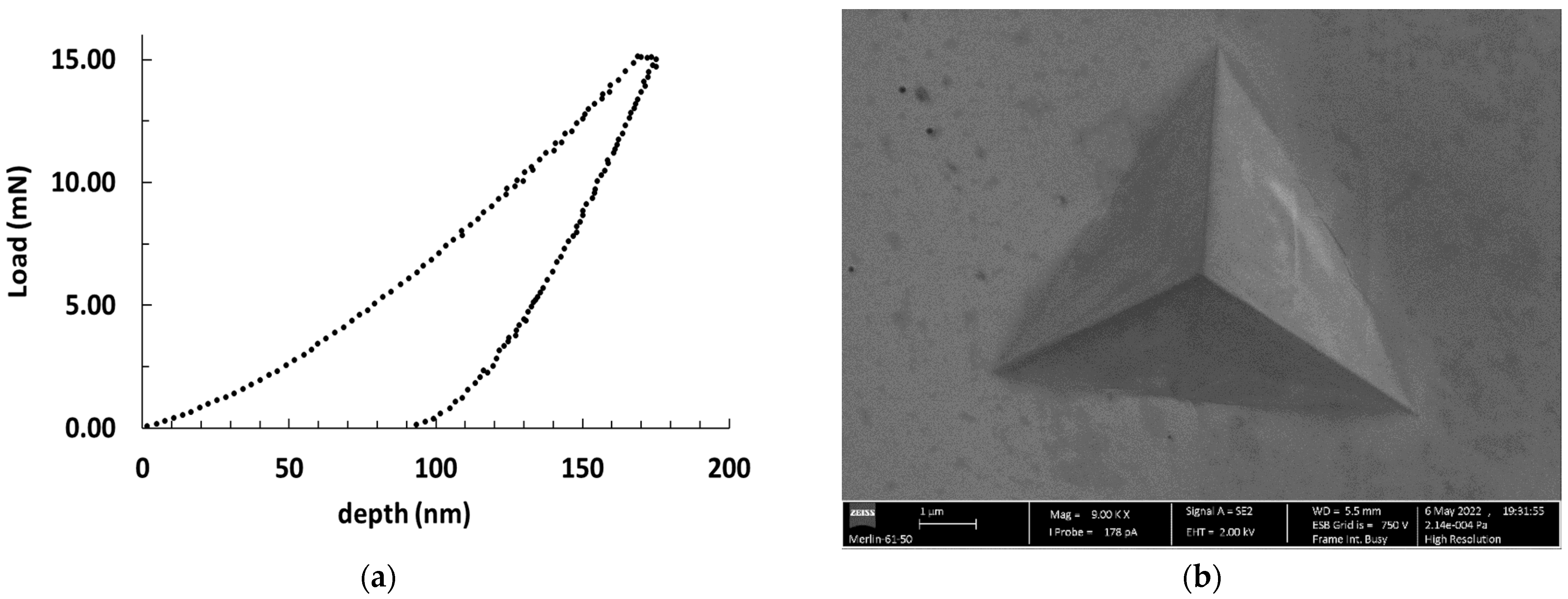
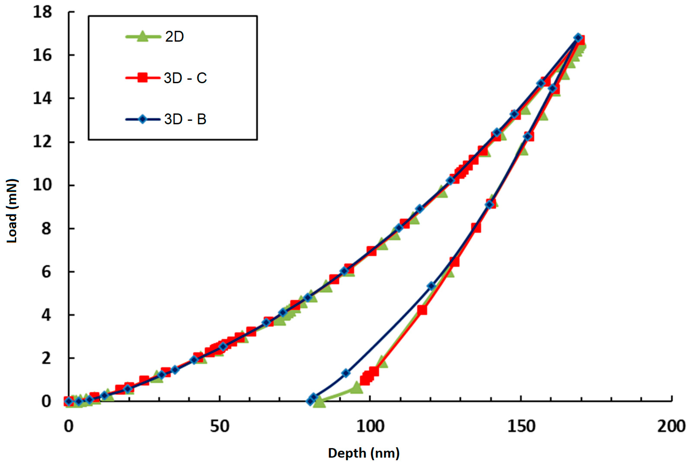
2.2. Nanoindentation Experiments

Nanoindentation experiments were conducted using a NanoTestTM NT1 nanoindentation instrument (NanoMaterials, Ltd., Wrexham, UK), which was equipped with a diamond pyramid-shaped Berkovich-type indenter. The Berkovich indenter has a three-sided pyramidal shape with a half angle of 65.3°. Prior to the measurements, the nanoindentation system was fully calibrated using fused silica as a standard sample. The tip-end curvature radius of the Berkovich indenter was determined using Hertzian analysis, yielding a value of 500 nm. All nanoindentation tests were performed at room temperature, using the load rate-control mode. The maximum applied loads (Pmax) reached up to 15 mN. To ensure the reproducibility of the results, a minimum of twenty independent tests were conducted on the GaN sample. During the nanoindentation tests, the maximum load was held constant for a dwell period of 30 s to account for the thermal drift. Additionally, to prevent interference between neighboring indents, each indentation was spaced apart by 30 μm. Notably, all indentation depths remained below 10% of the film thickness, guaranteeing that the influence of the sapphire substrate on the properties of the GaN film was negligible.

3. Identification Methodology

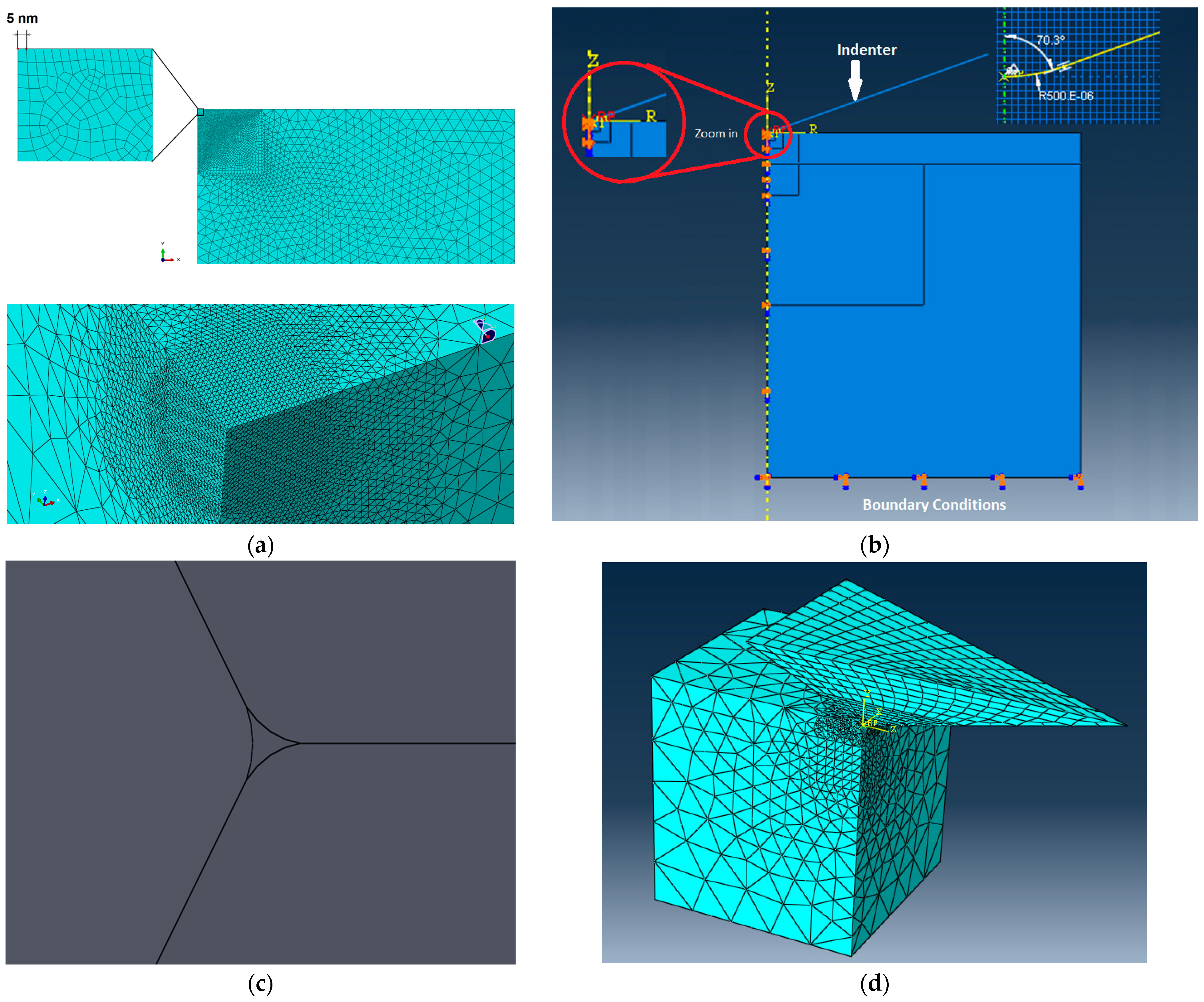
3.1. Finite Element Modeling

Finite element modeling (FEM) has emerged as the leading and most prevalent technique for simulating the nanoindentation process [36,37]. Finite element analysis is used to simulate the elastoplastic behavior of the GaN thin film. The numerical model is built and employed to produce datasets of nanoindentation load–depth curves. The mechanical responses are obtained based on various ranges of the elastoplastic material properties of the GaN thin film. To better account for the realistic contact between the indenter and the indentation imprint, three FE models are built. First, a 2D axisymmetric model is considered with a 2D equivalent conical-shaped Berkovich indenter. Second, a 3D model is developed with a 3D equivalent conical-shaped Berkovich indenter. Finally, a 3D model is constructed using a 3D Berkovich indenter by considering the indenter tip radius. The accuracy of the models’ response is recorded along with the computational time cost, for the purpose of comparison. FE models are constructed using ABAQUS Standard. In these FE models, thin films are assumed as deformable semi-infinite media, and the maximum indenter depth is kept shallow regarding the total film thickness. However, seeking simplicity, the indenter is assumed as a rigid body [38,39]. This assumption simplifies the computational model by negating the need to account for indenter deformation. The rationale behind this assumption lies in the significant stiffness disparity between the indenter, such as a diamond indenter in this study, and the GaN sample material. However, there are some examples of materials (as a general rule, we refer here to materials with an elastic stiffness more than 10% of that of the indenter and a yield strain higher than 1%, as well as to penetration depths less than ~5 times the characteristic tip defect length of the indenter) where accounting for the indenter deformation is important to obtain accurate hardness and modulus values [40]. The appropriate boundary conditions are applied depending on the used FE model among the three built models. For all models, the nodes on the bottom are subjected to fixed boundary conditions. Notably, mesh refinement is particularly applied in the region underneath the indenter, where very small elements of around 5 nanometers of size are used. But, as being far away from the indentation zone, the element size is gradually augmented to reduce time computation without losing the accuracy of the simulation results.
The 2D axisymmetric model is constructed using a total of 8353, 4-node bilinear elements with reduced integration (CAX4R) and 7922 nodes (see Figure 1a, top). The indenter in the axisymmetric assumption is an equivalent conical-shaped Berkovich indenter with a half angle of 70.3°, as the projected area is identical to that of the original pyramidal Berkovich indenter [41]. The conical-shaped Berkovich indenter is featured by a tip radius of 500 nm equivalent to the indenter tip radius used in experimental nanoindentation tests. As illustrated in Figure 1b, specific boundary conditions are applied to this type of FE model. The bottom surface of the deformed media is fixed for all degree of freedom (i.e., fixed boundary condition is implemented), while axisymmetric boundary conditions are applied to the left side in the z-direction. A reference point (RF) is defined to represent the rigid body indenter, and a displacement of 170 nm is associated with this reference point. Furthermore, the contact between the indenter and the film imprint is modeled using the implemented *surface to surface contact condition in Abaqus. The friction is taken into consideration using the penalty method [42]. The 3D FE model with a 3D equivalent conical-shaped Berkovich indenter is built using a 10-node quadratic tetrahedron (the C3D10 element in Abaqus) that offers high accuracy for complex geometries. This makes it a preferred choice for 3D FE nanoindentation simulations where capturing the precise contact mechanics between the indenter and the material is vital. For symmetry reasons, one-quarter of the model was considered and defined by 119,005 nodes and a total of 83,443 elements (see Figure 1a, bottom). The 3D equivalent conical-shaped Berkovich indenter is a 3D analytic rigid body defined by a half angle of 70.3° and a tip radius of 500 nm. The third FE model is a 3D FE model with a Berkovich indenter featured by a tip radius of 500 nm (see Figure 1c). The deformable part of the FE model is similar to the second model; however, the indenter is a discrete rigid body and meshed using C3D4, a 4-node linear tetrahedral element. Figure 1d shows the complete 3D FE model used to run nanoindentation simulations. The thin film behavior is assumed as elastoplastic with isotropic linear elastic behavior and obeys von Mises yield criterion and the isotropic strain hardening law of Swift-type.

3.2. Elastoplastic Constitutive Model

Commonly, the uniaxial tensile test carried out on a dog-bone sample (at millimetric scale) is used to characterize the mechanical behavior of bulk materials and accurately provide the stress–strain curve. However, for thin films, this conventional method is not suitable due to limitations in their applicability at micro/nanometric scales. Alternative techniques, such as nanoindentation, are necessary to obtain the appropriate mechanical properties.
In this study, we assume that the GaN material behavior obeys the class of elastoplastic materials, for which the total strain is decomposed into elastic and plastic parts, as given in Equation (1).
ε = ε y + ε p
where ε , ε y , and ε p represent the total, elastic, and plastic strains.
Commonly, to analyze the elastoplastic behavior of various materials, by investigating the inverse analysis of materials using nanoindentation, the assumption for isotropic materials is employed. This assumption relates the stress and strain through a piecewise function, as given in Equation (2).
σ = E ε   ( σ σ y ) K ε n   ( σ σ y )
where E, σ y , K, and n are the Young’s modulus, the yield stress, the hardening modulus, and the hardening exponent, respectively. In the plastic regime, the flow stress, representing the elastoplastic behavior, could be expressed by the following equation.
σ = σ y 1 + E σ y ε p n

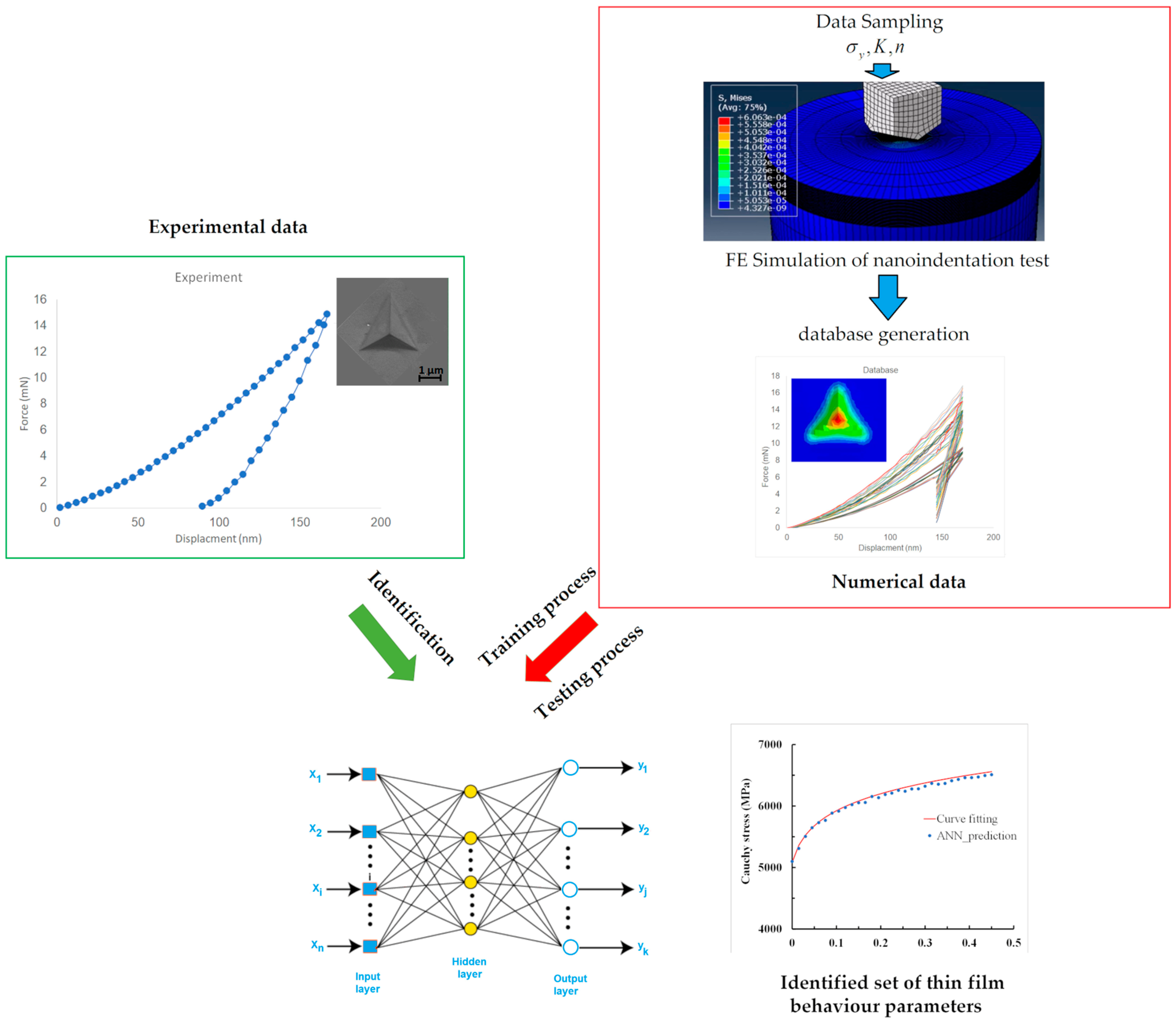
3.3. Data Sampling and Database Generation

Data sampling for generating a database is an essential step in the development of ANN models. The goal of data sampling is to select a representative set of data that can be used to train, test, and validate ANN models. The Box–Behnken design (BBD) is a type of experimental design that can be used for efficient data sampling from a high-dimensional space. The BBD is a fractional factorial design that is rotatable, meaning that the effects of the factors are not confounded. This makes the BBD a good choice for sampling data for ANN training, testing, and validation, as it ensures that the effects of the factors are accurately estimated [43]. The BBD is used to obtain the design matrix of the FE simulations. Table 1 lists the design matrix used to generate the FE results of the nanoindentation of the GaN thin film. In this work, the generated FE dataset contains 81 load–depth curves corresponding to the maximum applied load of 15 mN. Then, 25 data points are used for each curve, among them, the total work to the plastic work ratio (Wp/Wt) and the stiffness (dP/dh) are included along with (P-h) data to consider with accuracy the indentation information of the unloading curve (see Figure 2). Therefore, a matrix of [25 × 81] is introduced as inputs in the ANN model.

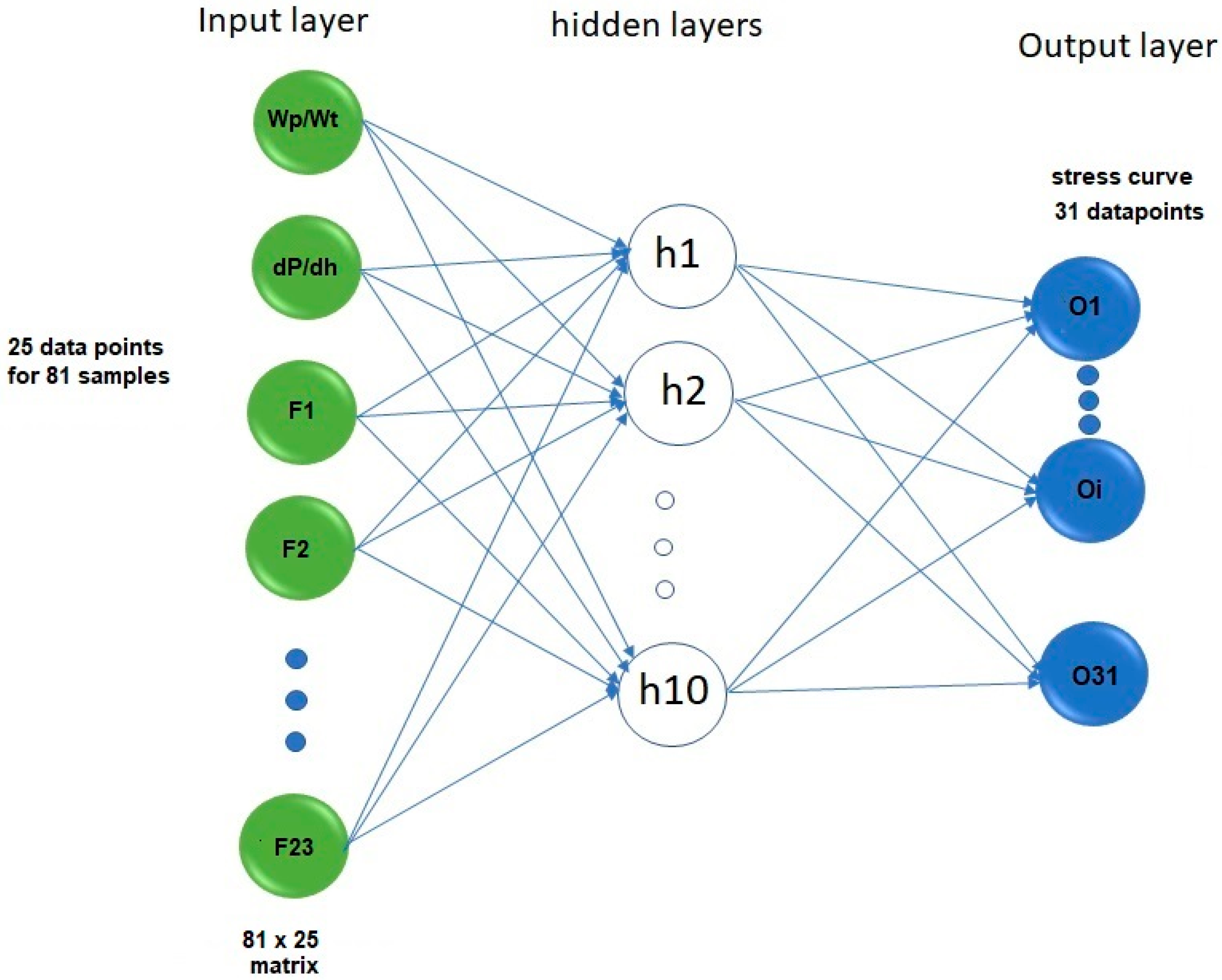
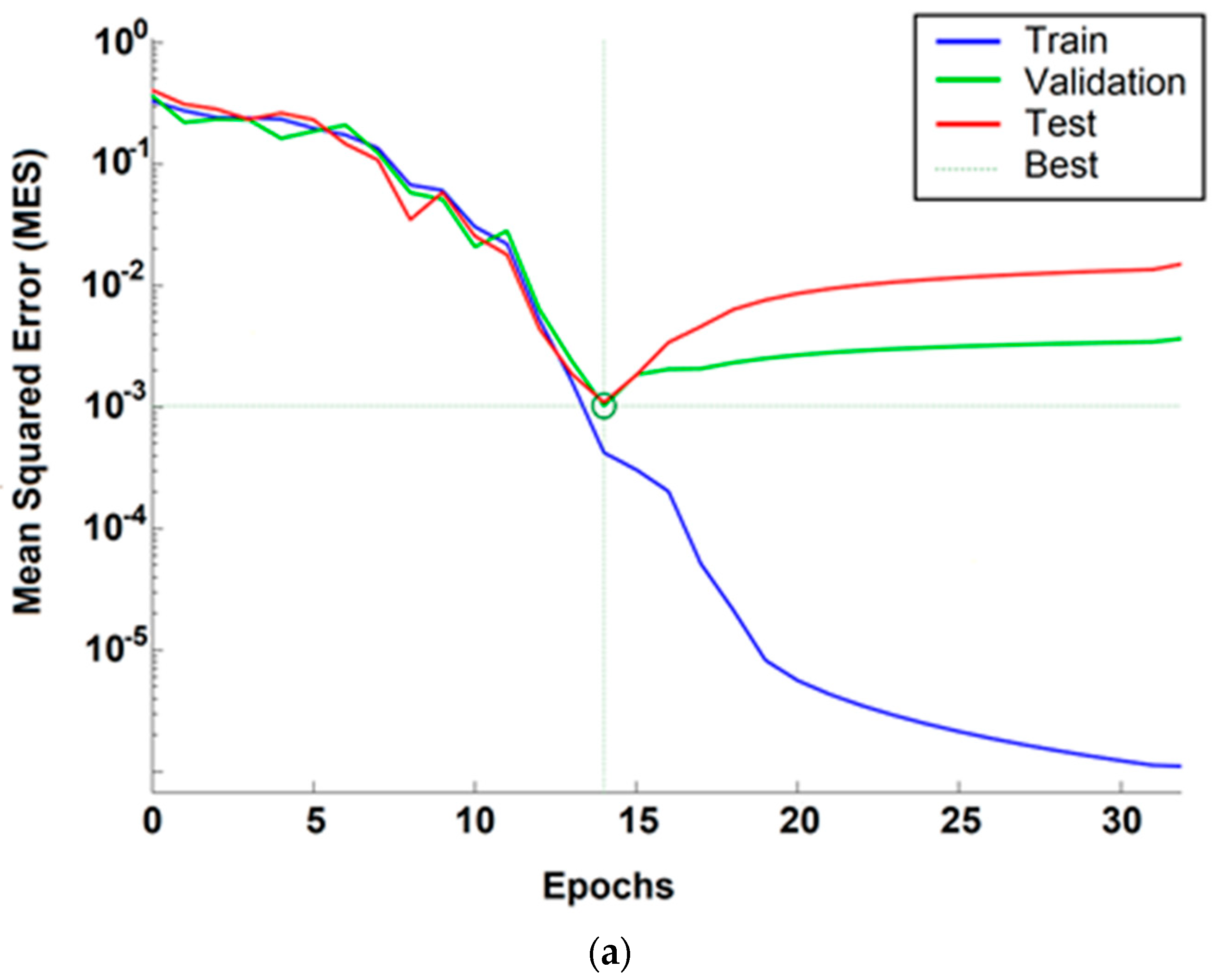
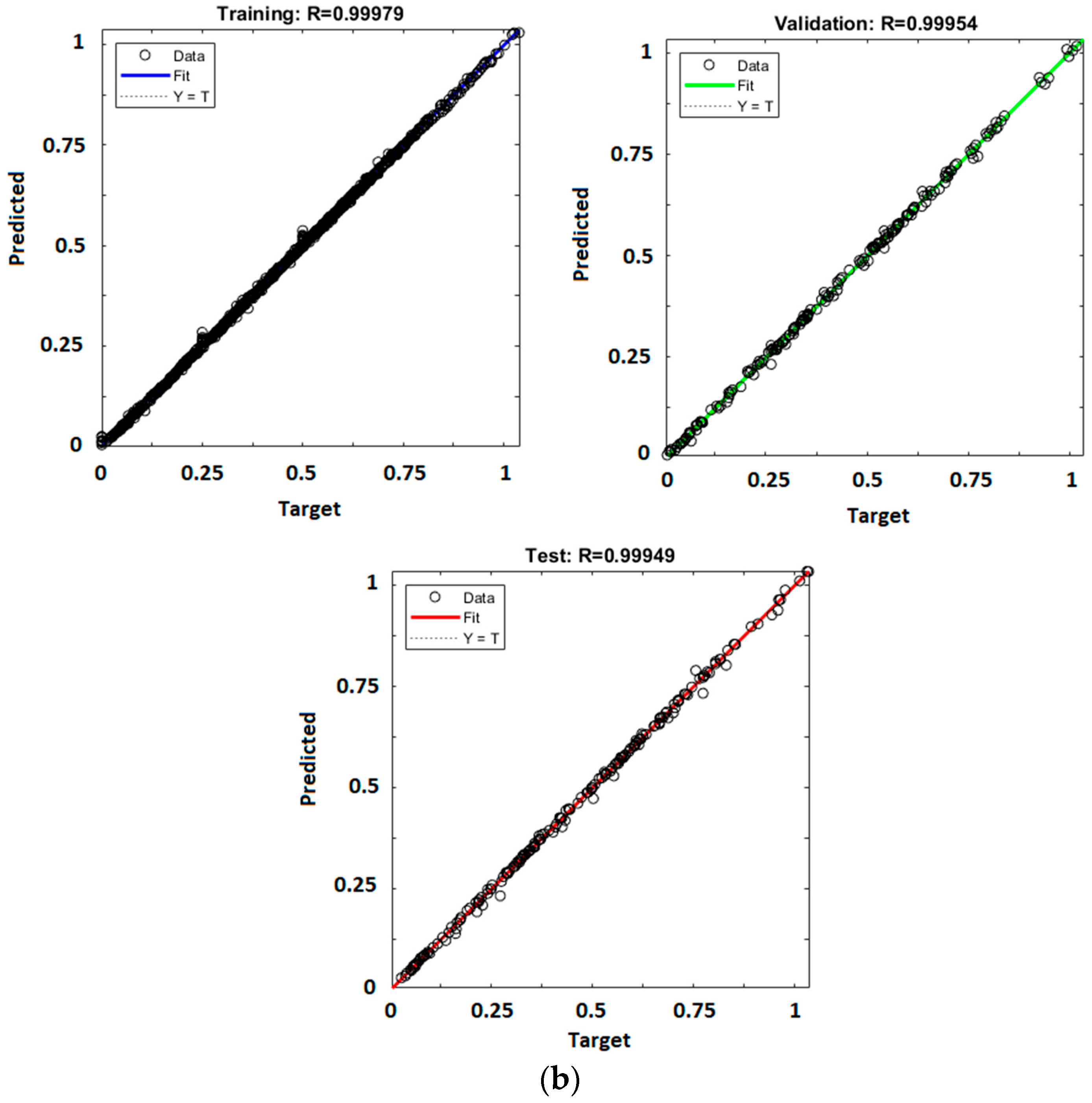
3.4. Artificial Neural Network (ANN)

Artificial neural networks (ANNs) are a type of supervised machine learning (ML) algorithms that are inspired by the human brain. They are composed of interconnected nodes, called neurons, that learn to process information and make predictions by adjusting their weights and biases during the training process. The performance of an ANN is based on the quality of the training data and the number of neurons and layers in the network. This allows for the construction of a functional dependency between inputs and outputs. In this work, we developed an inverse analysis method for identifying the elastoplastic parameters of GaN thin films using an ANN model which learns from simulated nanoindentation load–depth curves.
Figure 2 shows the feed-forward ANN structure with one hidden layer connecting the input and output layers. It is worth noting that the performance of the ANN model substantially depends on the number of neurons in the hidden layer and the learning rate. Therefore, a trial-and-error method was used to tune these parameters for the better accuracy of the ANN model. The training sets uses backpropagation with the Levenberg-Marquardt (LM) algorithm to update and determine the weights and biases of the neurons of the ANN model. The activation functions used in the hidden and output layer are the Logarithmic sigmoid (Logsig) and linear (Purelin) function, respectively. The input and output datasets were normalized using a linear transformation. This normalization was achieved to improve the training speed of the ANN model and to reduce the chances of the model becoming trapped in local minima. Additionally, normalization helps to prevent the ANN model from finding multiple solutions to the inverse problem [44,45].
It is important to note that the use of a limited number of training datasets for an ANN model can make it difficult to obtain an effective network predictivity. However, it is possible to train ANN models with limited datasets using regularization techniques, such as either Bayesian regularization [46] or the early stopping method to avoid the problem of ANN overfitting. Overfitting is a critical issue that can affect an ANN model’s performance, when the ANN model prioritizes fitting the training data too precisely, at the expense of its ability to generalize well to new, unseen data. Bayesian regularization does not require a validation subset, but it is more computationally expensive. In this work, the so-called early stopping method is used to avoid the overfitting of the network during the training process. Therefore, this method is used to improve the generalization performance of the network. The input datasets are randomly divided into three subsets: the training, validation, and testing subsets. The training subset is used to learn the ANN model, the validation subset is used to assess the generalization capacity of the model, and the testing subset is used to assess the performance of the model on unknown data. The input dataset is randomly partitioned into 70% for training, 15% for validation, and 15% for testing. The error on the validation set is monitored during the training process. The training stops automatically when the validation error starts to increase instead of continuously decreasing the validation data’s mean square error (MSE). To verify the performance and effectiveness of the network learning, additional virtual responses were randomly generated using a finite element model. The parameters of these virtual responses were known and within the range of the considered parameters. These virtual responses were then used as extra virtual experimental inputs in the trained ANN model, assuming that the corresponding parameters were unknown. This is an effective way to re-evaluate the performance capacity of the trained network using additional input datasets that are unknown to the network, thus avoiding multiple solutions to the inverse problem. More details about the feature of the used ANN model are summarized in Table 2.
Figure 3 shows the flowchart of the inverse identification approach used in this work to identify the stress–strain curve of the elastoplastic behavior. The identification procedure can be described in the following steps: firstly, the experimental data (load–depth nanoindentation curve) are obtained through the averaging of twenty experimental nanoindentation tests; secondly, a highly accurate finite element model is built for the numerical simulation of the nanoindentation; thirdly, data sampling was performed based on the BBD to determine and prepare the sets of the data inputs for the FE model to generate the numerical datasets; and fourthly, the dataset of the numerical load–depth curves is applied for the training, validation, and test procedures.

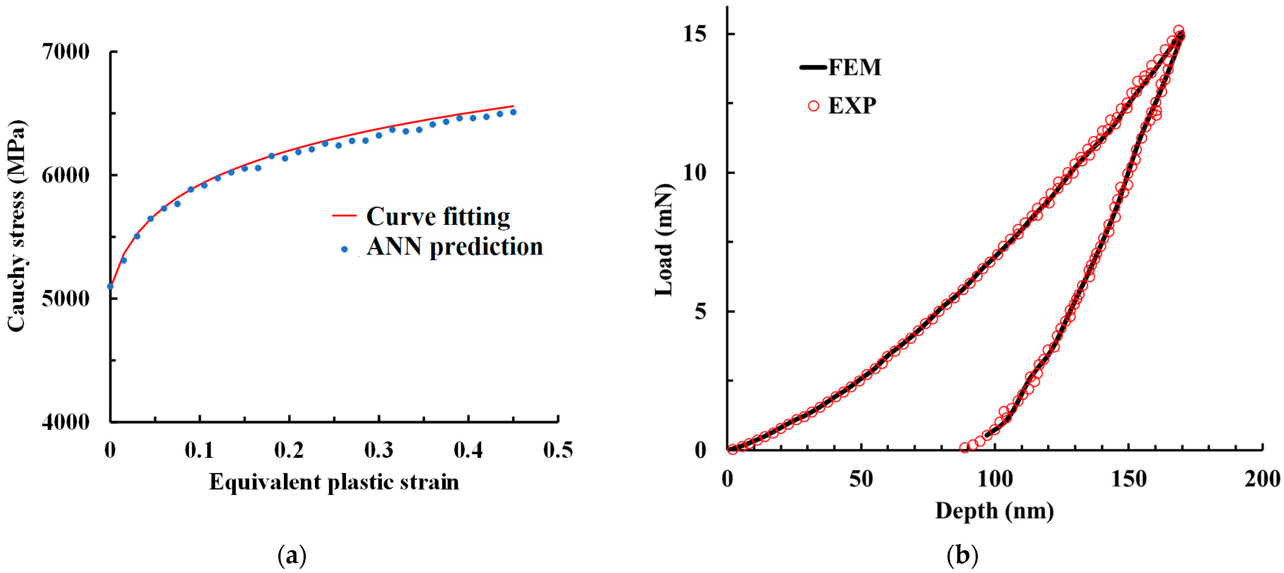
4. Results and Discussion

Figure 4a shows the averaged curve over the twenty experimental load–depth curves. Furthermore, the scanning electron microscopy (SEM) image depicts the indentation imprint on the GaN sample obtained by applying a load of 500 mN on the Berkovich indenter, as displayed in Figure 4b. Table 3 lists, for the GaN thin film and the sapphire substrate, the hardness and the Young’s modulus. The mechanical properties of the GaN thin film are obtained from analyzing the experimental load–depth curves using the Oliver–Pharr method. This table also presents the elastic recovery (i.e., which refers to the amount of deformation that the material recovers elastically after the indenter has been removed) along with the maximum applied load and the resulting maximal depth recorded at this load. In comparison, the sapphire substrate exhibits higher mechanical properties compared to GaN. The substrate’s hardness is reported as 27.5 ± 2 GPa, with an elastic modulus of 420.6 ± 20 GPa. The specific data regarding the maximum load, maximum depth, and elastic recovery for the sapphire substrate are not available.
Figure 5 shows the numerical load–depth curves obtained using the three finite element models: (i) 2D axisymmetric, (ii) 3D equivalent conical-shaped Berkovich indenter, and (iii) 3D Berkovich indenter (see Figure 1). The three models exhibit comparable predictive capabilities regarding the nanoindentation load curve. The unload curve demonstrates a high degree of similarity. Nevertheless, at the end of the unloading phase, the 3D Berkovich model displays minor deviations from the prediction of both the 2D axisymmetric and 3D equivalent conical-shaped Berkovich indenter models. Notably, the use of the 3D Berkovich model demands significant computational resources and time. In pursuit of an optimal balance between computational accuracy and efficiency, it becomes evident that the 2D axisymmetric model emerges as the preferred choice. Therefore, this model is adopted to conduct the finite element simulations of nanoindentation tests in the subsequent analyses.
To decouple material properties from the influence of factors like the friction coefficient and indenter tip radius in the case of nanoindentation, Figure 6 presents an analysis of the numerical model’s response to variations in these factors. By assessing their effects using nanoindentation simulations, we can gain valuable insights into the actual mechanical behavior of the thin films characterized by nanoindentation. This allows us to understand the sensitivity of the FE model to changes in these critical variables, providing a more nuanced interpretation of the results and their implications on experimental nanoindentation data. Figure 6a depicts that the friction coefficient has no visible effect on the nanoindentation load–depth curve, even for high values. This is because friction primarily affects lateral forces and frictional interactions between the indenter and the film’s contact surface. While friction may influence the lateral frictional force during loading and unloading phases, it typically has a negligible impact on the overall vertical force–displacement relationship captured by the load–depth curve, as also reported by Wang [48]. In contrast, Figure 6b clearly shows the visual influence of the indenter tip radius on the nanoindentation curve. The curves depict the results for several distinct tip radii, ranging from 50 nm to 500 nm. As the curves reach the same indentation depth (e.g., the simulations are run using imposed displacement), the load values differ significantly. Notably, the curve representing the smaller tip radius (50 nm) exhibits a lower load compared to the larger tip radius (500 nm) at the same depth. This behavior arises from the varying contact area created by different tip geometries. The larger tip with a 500 nm radius distributes the applied force over a broader area, necessitating a higher overall load to achieve the same level of indentation compared to the sharper tip that concentrates the force on a smaller area. Wang [48] reported that the change in the tip radius results in a significant effect on the load displacement data. The authors found the load to increase with a larger tip radius at the same maximum indentation depth. The sensitivity of the load–depth response to the indenter tip radius underscores a limitation of the rigid indenter assumption in nanoindentation simulations. While this assumption simplifies calculations, it neglects tip deformation, which becomes more pronounced as indenter radii decrease and loads increase. This can result in inaccurate load–depth relationships, errors in extracted mechanical properties, and misinterpretations of material behavior. However, when the indenter tip radius is sufficiently large, the assumption of using a rigid indenter in finite element analysis is valid, as shown in this work.
Figure 7a shows the training performance of the ANN model over epochs. It includes three lines, one representing the training set error (in blue), the validation set error (green line), and the test set error (red line). The mean squared error (MSE) of the training set decreases steadily, indicating improvement in the ANN model’s performance on the training set. The MSE of the validation and the test processes are also decreasing but with more fluctuations, suggesting improvement in the model’s performance on the validation set and test set with some variability. The best performance of the ANN model is achieved with the lowest mean squared error (MSE) for the validation and test sets at approximately 1.022 × 10⁻³. The increase trend after the 14th epoch of the MSE of the validation set indicates an overfitting issue of the ANN model. Therefore, the early stopping regularization method is activated to avoid overfitting, which reduces the ANN model’s performance. This MSE plot is a metric used to monitor the model’s learning progress, aiming to minimize errors on the training, validation, and test sets. Figure 7b displays the R-plots, which illustrate the regression analysis, showcasing the correlation between the target and the actual outputs of the ANN model. The linear regression coefficients of the training and validation and test processes are depicted during the network’s learning process. The correlation coefficient (R) value of 0.999 (approaching 1) is attained, signifying strong correlation. Additionally, the minimum MSE value is achieved, while the overfitting of the ANN model is mitigated by applying the early stopping regularization method, as shown in Figure 7a, indicating the construction of the high-performance ANN model, ready to be used for prediction for input experimental data.
Figure 8 exhibits the stress–strain curve determined using the developed ANN model and the verification of the capacity of the obtained stress–strain curve to produce the experimental responses using finite element simulation. Figure 8a showcases the stress–strain data (blue solid circles “”) predicted by the ANN model and using the experimental load–depth data as input in the trained ANN model. The red line (“”) represents the curve fitting of the data points using the elastoplastic constitutive model (power law model) given in Equation (3). It is noted that this curve fitting is in quite good agreement with the data points. The material parameters obtained based on the stress–strain curve fitting are listed in Table 4.
Figure 8b displays the comparison between the experimental load–depth curve and the curve obtained by numerical simulation using the stress–strain curve identified by the ANN model (data points). This result ascertains the performance of the used identification procedure to determine the elastoplastic behavior of the GaN thin film. It is clearly observed that the curve calculated by the finite element method is in very good agreement with the experimental curve. This represents a good verification of the obtained solution, which reflects the accuracy and performance of the developed inverse identification-based ANN model for deducing the constitutive equation of thin film using nanoindentation experiments. Furthermore, it could be mentioned that the ratio between the measured hardness H and the identified yield stress σ y approximately verifies the empirical well-known Tabor formula (H ≈ 3 × σ y ), which is the most applicable for relatively hard materials like metals and ceramics, where plastic deformation dominates the indentation response. It is worth noting that the identified Young’s modulus (365.4 GPa) is relatively close to the measured value (356 ± 8 GPa), determined from nanoindentation experiments using the Oliver–Pharr approach. On the other hand, the power law exponent with a value of 0.073 is very small. This low value is likely attributed to the dominant plasticity mechanisms occurring during the nanoindentation process. This behavior reflects the weak work-hardening exhibited by the GaN thin film material, which is commonly observed, at nanoscale, in stress–strain curves for ceramics and metals. In molecular dynamic (MD) simulations of metallic behavior at the atomistic scale, near-perfect plasticity (plastic flow with shallow strain hardening) is often found [49,50]. Subsequently, it is noteworthy that the identified behavior model (Equation (3)) is an empirical power law equation typically used to describe the elastoplastic behavior of metallic materials at the macroscale. In this study, we applied this equation to assess its capability in describing the mechanical behavior of a thin film at the nanoscale. Further investigation using MD simulations could provide valuable insights into the plastic behavior and potentially reveal correlations with the analysis based on macroscale relations. Furthermore, it is suggested to couple the finite element model with an MD model to thoroughly study material behaviors at different length scales.

5. Conclusions

This study demonstrated the effectiveness of an inverse identification approach using artificial neural networks (ANNs) for extracting the elastoplastic parameters of GaN thin films from load–depth nanoindentation data. Three finite element models were built and evaluated, revealing that a 2D axisymmetric model could accurately replicate the computationally expensive 3D model’s outputs. However, the load–depth response remained sensitive to the indenter tip radius, highlighting the importance of considering this factor in the simulation of nanoindentation for enhanced result accuracy. The trained/validated ANN model, built upon the 2D model-generated database, successfully predicted the GaN thin film’s stress–strain curve. The verification capacity of this stress–strain curve in describing the elastoplastic behavior of the GaN thin film was achieved through a finite element simulation of the nanoindentation test. The excellent performance of the developed ANN model underscores its capability to predict the actual stress–strain curve of the GaN thin film based on experimental nanoindentation data. This approach offers a computationally efficient and accurate method for identifying elastoplastic parameters of thin films, leveraging the combined power of nanoindentation testing, finite element simulations, and ANNs.

Author Contributions

Conceptualization, methodology, and software, A.K. (Ali Khalfallah), A.K. (Amine Khalfallah), and Z.B.; validation, A.K. (Ali Khalfallah) and Z.B.; formal analysis, A.K. (Ali Khalfallah); investigation, A.K. (Amine Khalfallah) and Z.B.; data curation, A.K. (Amine Khalfallah) and Z.B.; writing—original draft preparation, A.K. (Ali Khalfallah); writing—review and editing, A.K. (Ali Khalfallah) and Z.B.; visualization. All authors have read and agreed to the published version of the manuscript.

Funding

This research received no external funding.

Institutional Review Board Statement

Not applicable.

Informed Consent Statement

Not applicable.

Data Availability Statement

Data are available on request.

Conflicts of Interest

The authors declare no conflicts of interest.

References

  1. Touré, A.; Halidou, I.; Benzarti, Z.; Fouzri, A.; Bchetnia, A.; El Jani, B. Characterization of Low Al Content AlxGa1−xN Epitaxial Films Grown by Atmospheric-Pressure MOVPE. Phys. Status Solidi 2012, 209, 977–983. [Google Scholar] [CrossRef]
  2. Benzarti, Z.; Khalfallah, A.; Bougrioua, Z.; Evaristo, M.; Cavaleiro, A. Understanding the Influence of Physical Properties on the Mechanical Characteristics of Mg-Doped GaN Thin Films. Mater. Chem. Phys. 2023, 307, 128182. [Google Scholar] [CrossRef]
  3. Benzarti, Z.; Sekrafi, T.; Bougrioua, Z.; Khalfallah, A.; El Jani, B. Effect of SiN Treatment on Optical Properties of InxGa1−xN/GaN MQW Blue LEDs. J. Electron. Mater. 2017, 46, 4312–4320. [Google Scholar] [CrossRef]
  4. Bayram, C.; Shiu, K.T.; Zhu, Y.; Cheng, C.W.; Sadana, D.K.; Teherani, F.H.; Rogers, D.J.; Sandana, V.E.; Bove, P.; Zhang, Y.; et al. Engineering Future Light Emitting Diodes and Photovoltaics with Inexpensive Materials: Integrating ZnO and Si into GaN-Based Devices. Oxide-Based Mater. Devices IV 2013, 8626, 86260L. [Google Scholar] [CrossRef]
  5. Prado, E.O.; Bolsi, P.C.; Sartori, H.C.; Pinheiro, J.R. An Overview about Si, Superjunction, SiC and GaN Power MOSFET Technologies in Power Electronics Applications. Energies 2022, 15, 5244. [Google Scholar] [CrossRef]
  6. Runton, D.W.; Trabert, B.; Shealy, J.B.; Vetury, R. History of GaN: High-Power RF Gallium Nitride (GaN) from Infancy to Manufacturable Process and Beyond. IEEE Microw. Mag. 2013, 14, 82–93. [Google Scholar] [CrossRef]
  7. Lin, J.T.; Wang, P.; Shuvra, P.; McNamara, S.; McCurdy, M.; Davidson, J.; Walsh, K.; Alles, M.; Alphenaar, B. Impact of X-ray Radiation on GaN/AlN MEMS Structure and GaN HEMT Gauge Factor Response. In Proceedings of the 2020 IEEE 33rd International Conference on Micro Electro Mechanical Systems (MEMS), Vancouver, BC, Canada, 18–22 January 2020; pp. 968–971. [Google Scholar] [CrossRef]
  8. Ambacher, O.; Eickhoff, M.; Link, A.; Hermann, M.; Stutzmann, M.; Bernardini, F.; Fiorentini, V.; Smorchkova, Y.; Speck, J.; Mishra, U.; et al. Electronics and Sensors Based on Pyroelectric AlGaN/GaN Heterostructures: Part A: Polarization and Pyroelectronics. Phys. Status Solidi C Conf. 2003, 1878–1907. [Google Scholar] [CrossRef]
  9. Lv, L.; Ma, J.G.; Cao, Y.R.; Zhang, J.C.; Zhang, W.; Li, L.; Xu, S.R.; Ma, X.H.; Ren, X.T.; Hao, Y. Study of Proton Irradiation Effects on AlGaN/GaN High Electron Mobility Transistors. Microelectron. Reliab. 2011, 51, 2168–2172. [Google Scholar] [CrossRef]
  10. Rocco, E.; Licata, O.; Mahaboob, I.; Hogan, K.; Tozier, S.; Meyers, V.; McEwen, B.; Novak, S.; Mazumder, B.; Reshchikov, M.; et al. Hillock Assisted P-Type Enhancement in N-Polar GaN:Mg Films Grown by MOCVD. Sci. Rep. 2020, 10, 1426. [Google Scholar] [CrossRef]
  11. Azimah, E.; Zainal, N.; Hassan, Z.; Shuhaimi, A.; Bahrin, A. Electrical and Optical Characterization of Mg Doping in GaN. Adv. Mater. Res. 2013, 620, 453–457. [Google Scholar]
  12. Boughrara, N.; Benzarti, Z.; Khalfallah, A.; Evaristo, M.; Cavaleiro, A. Comparative Study on the Nanomechanical Behavior and Physical Properties Influenced by the Epitaxial Growth Mechanisms of GaN Thin Films. Appl. Surf. Sci. 2022, 579, 152188. [Google Scholar] [CrossRef]
  13. Tsai, C.H.; Jian, S.R.; Juang, J.Y. Berkovich Nanoindentation and Deformation Mechanisms in GaN Thin Films. Appl. Surf. Sci. 2008, 254, 1997–2002. [Google Scholar] [CrossRef]
  14. Khalfallah, A.; Benzarti, Z. Mechanical Properties and Creep Behavior of Undoped and Mg-Doped GaN Thin Films Grown by Metal–Organic Chemical Vapor Deposition. Coatings 2023, 13, 1111. [Google Scholar] [CrossRef]
  15. Laxmikant Vajire, S.; Prashant Singh, A.; Kumar Saini, D.; Kumar Mukhopadhyay, A.; Singh, K.; Mishra, D. Novel Machine Learning-Based Prediction Approach for Nanoindentation Load-Deformation in a Thin Film: Applications to Electronic Industries. Comput. Ind. Eng. 2022, 174, 108824. [Google Scholar] [CrossRef]
  16. Peng, L.; Liu, F.; Ni, J.; Lai, X. Size Effects in Thin Sheet Metal Forming and Its Elastic–Plastic Constitutive Model. Mater. Des. 2007, 28, 1731–1736. [Google Scholar] [CrossRef]
  17. Raulea, L.V.; Goijaerts, A.M.; Govaert, L.E.; Baaijens, F.P.T. Size Effects in the Processing of Thin Metal Sheets. J. Mater. Process. Technol. 2001, 115, 44–48. [Google Scholar] [CrossRef]
  18. Pathak, S.; Kalidindi, S.R. Spherical Nanoindentation Stress-Strain Curves. Mater. Sci. Eng. R. Rep. 2015, 91, 1–36. [Google Scholar] [CrossRef]
  19. Golovin, Y.I. Nanoindentation and Mechanical Properties of Solids in Submicrovolumes, Thin near-Surface Layers, and Films: A Review. Phys. Solid State 2008, 50, 2205–2236. [Google Scholar] [CrossRef]
  20. Liu, K.; Ostadhassan, M.; Bubach, B. Applications of Nano-Indentation Methods to Estimate Nanoscale Mechanical Properties of Shale Reservoir Rocks. J. Nat. Gas Sci. Eng. 2016, 35, 1310–1319. [Google Scholar] [CrossRef]
  21. Boughrara, N.; Benzarti, Z.; Khalfallah, A.; Oliveira, J.C.; Evaristo, M.; Cavaleiro, A. Thickness-Dependent Physical and Nanomechanical Properties of AlxGa1−xN Thin Films. Mater. Sci. Semicond. Process. 2022, 151, 107023. [Google Scholar] [CrossRef]
  22. Jian, S.R.; Tasi, C.H.; Huang, S.Y.; Luo, C.W. Nanoindentation Pop-in Effects of Bi2Te3 Thermoelectric Thin Films. J. Alloys Compd. 2015, 622, 601–605. [Google Scholar] [CrossRef]
  23. Zhou, G.; Guo, J.; Zhao, J.; Tang, Q.; Hu, Z. Nanoindentation Properties of 18CrNiMo7-6 Steel after Carburizing and Quenching Determined by Continuous Stiffness Measurement Method. Metals 2020, 10, 125. [Google Scholar] [CrossRef]
  24. Ohmura, T.; Wakeda, M. Pop-In Phenomenon as a Fundamental Plasticity Probed by Nanoindentation Technique. Materials 2021, 14, 1879. [Google Scholar] [CrossRef]
  25. Qian, L.; Zhao, H. Nanoindentation of Soft Biological Materials. Micromachines 2018, 9, 654. [Google Scholar] [CrossRef]
  26. Li, Y.; Li, S. Deep Learning Based Phase Transformation Model for the Prediction of Microstructure and Mechanical Properties of Hot-Stamped Parts. Int. J. Mech. Sci. 2022, 220, 107134. [Google Scholar] [CrossRef]
  27. Sun, X.; Liu, Z.; Wang, X.; Chen, X. Determination of Ductile Fracture Properties of 16MND5 Steels under Varying Constraint Levels Using Machine Learning Methods. Int. J. Mech. Sci. 2022, 224, 107331. [Google Scholar] [CrossRef]
  28. Merayo, D.; Rodríguez-Prieto, A.; Camacho, A.M. Prediction of Mechanical Properties by Artificial Neural Networks to Characterize the Plastic Behavior of Aluminum Alloys. Materials 2020, 13, 5227. [Google Scholar] [CrossRef]
  29. Long, X.; Dong, R.; Su, Y.; Chang, C. Critical Review of Nanoindentation-Based Numerical Methods for Evaluating Elastoplastic Material Properties. Coatings 2023, 13, 1334. [Google Scholar] [CrossRef]
  30. Li, Z.; Ye, Y.; Zhang, G.; Guan, F.; Luo, J.; Wang, P.; Zhao, J.; Zhao, L. Research on Determining Elastic–Plastic Constitutive Parameters of Materials from Load Depth Curves Based on Nanoindentation Technology. Micromachines 2023, 14, 1051. [Google Scholar] [CrossRef]
  31. Smith, J.L. Advances in Neural Networks and Potential for Their Application to Steel Metallurgy. Mater. Sci. Technol. 2020, 36, 1805–1819. [Google Scholar] [CrossRef]
  32. Park, S.; Fonseca, J.H.; Marimuthu, K.P.; Jeong, C.; Lee, S.; Lee, H. Determination of Material Properties of Bulk Metallic Glass Using Nanoindentation and Artificial Neural Network. Intermetallics 2022, 144, 107492. [Google Scholar] [CrossRef]
  33. Lu, L.; Dao, M.; Kumar, P.; Ramamurty, U.; Karniadakis, G.E.; Suresh, S. Extraction of Mechanical Properties of Materials through Deep Learning from Instrumented Indentation. Proc. Natl. Acad. Sci. USA 2020, 117, 7052–7062. [Google Scholar] [CrossRef]
  34. Jeong, K.; Lee, H.; Kwon, O.M.; Jung, J.; Kwon, D.; Han, H.N. Prediction of Uniaxial Tensile Flow Using Finite Element-Based Indentation and Optimized Artificial Neural Networks. Mater. Des. 2020, 196, 109104. [Google Scholar] [CrossRef]
  35. Wang, J.S.; Zheng, X.J.; Zheng, H.; Song, S.T.; Zhu, Z. Identification of Elastic Parameters of Transversely Isotropic Thin Films by Combining Nanoindentation and FEM Analysis. Comput. Mater. Sci. 2010, 49, 378–385. [Google Scholar] [CrossRef]
  36. Cheng, S.W.; Chen, B.S.; Jian, S.R.; Hu, Y.M.; Le, P.H.; Tuyen, L.T.C.; Lee, J.W.; Juang, J.Y. Finite Element Analysis of Nanoindentation Responses in Bi2Se3 Thin Films. Coatings 2022, 12, 1554. [Google Scholar] [CrossRef]
  37. Shui, S. Progress and Challenges in Finite Element Simulation of Nanoindentation of Ion-Irradiated Materials. J. Phys. Conf. Ser. 2021, 1885, 032039. [Google Scholar] [CrossRef]
  38. Bressan, J.D.; Tramontin, A.; Rosa, C. Modeling of Nanoindentation of Bulk and Thin Film by Finite Element Method. Wear 2005, 258, 115–122. [Google Scholar] [CrossRef]
  39. Barkachary, B.M.; Joshi, S.N. Numerical Simulation and Experimental Validation of Nanoindentation of Silicon Using Finite Element Method. In Advances in Computational Methods in Manufacturing: Select Papers from ICCMM 2019; Springer: Singapore, 2019; pp. 861–875. [Google Scholar] [CrossRef]
  40. Keryvin, V.; Charleux, L.; Bernard, C.; Nivard, M. The Influence of Indenter Tip Imperfection and Deformability on Analysing Instrumented Indentation Tests at Shallow Depths of Penetration on Stiff and Hard Materials. Exp. Mech. 2017, 57, 1107–1113. [Google Scholar] [CrossRef]
  41. Shi, Z.; Feng, X.; Huang, Y.; Xiao, J.; Hwang, K.C. The Equivalent Axisymmetric Model for Berkovich Indenters in Power-Law Hardening Materials. Int. J. Plast. 2010, 26, 141–148. [Google Scholar] [CrossRef]
  42. Lee, H.; Huen, W.Y.; Vimonsatit, V.; Mendis, P. An Investigation of Nanomechanical Properties of Materials Using Nanoindentation and Artificial Neural Network. Sci. Rep. 2019, 9, 13189. [Google Scholar] [CrossRef]
  43. Ktari, Z.; Leitão, C.; Prates, P.A.; Khalfallah, A. Mechanical Design of Ring Tensile Specimen via Surrogate Modelling for Inverse Material Parameter Identification. Mech. Mater. 2021, 153, 103673. [Google Scholar] [CrossRef]
  44. Nino-Adan, I.; Portillo, E.; Landa-Torres, I.; Manjarres, D. Normalization Influence on ANN-Based Models Performance: A New Proposal for Features’ Contribution Analysis. IEEE Access 2021, 9, 125462–125477. [Google Scholar] [CrossRef]
  45. Huang, L.; Qin, J.; Zhou, Y.; Zhu, F.; Liu, L.; Shao, L. Normalization Techniques in Training DNNs: Methodology, Analysis and Application. IEEE Trans. Pattern Anal. Mach. Intell. 2023, 45, 10173–10196. [Google Scholar] [CrossRef] [PubMed]
  46. Burden, F.; Winkler, D. Bayesian Regularization of Neural Networks. In Methods in Molecular Biology; Livingstone, D.J., Ed.; Humana Press: Totowa, NJ, USA, 2008; Volume 458, pp. 23–42. ISBN 9781588297181. [Google Scholar]
  47. Mao, W.G.; Shen, Y.G.; Lu, C. Nanoscale Elastic-Plastic Deformation and Stress Distributions of the C Plane of Sapphire Single Crystal during Nanoindentation. J. Eur. Ceram. Soc. 2011, 31, 1865–1871. [Google Scholar] [CrossRef]
  48. Wang, T.H.; Fang, T.H.; Lin, Y.C. A Numerical Study of Factors Affecting the Characterization of Nanoindentation on Silicon. Mater. Sci. Eng. A 2007, 447, 244–253. [Google Scholar] [CrossRef]
  49. Ivashchenko, V.I.; Turchi, P.E.A.; Shevchenko, V.I. Simulations of the Mechanical Properties of Crystalline, Nanocrystalline, and Amorphous SiC and Si. Phys. Rev. B—Condens. Matter Mater. Phys. 2007, 75, 085209. [Google Scholar] [CrossRef]
  50. Schiøtz, J.; Vegge, T.; Di Tolla, F.D.; Jacobsen, K.W. Atomic-Scale Simulations of the Mechanical Deformation of Nanocrystalline Metals. Phys. Rev. B—Condens. Matter Mater. Phys. 1999, 60, 11971–11983. [Google Scholar] [CrossRef]
Figure 1. Finite element models used in the numerical simulation of the nanoindentation (deformable parts): (a) the 2D axisymmetric FE model (top) and the 3D FE model (bottom) (deformable part); (b) the applied boundary conditions for the 2D FE model and definition of the 500 nm indenter tip radius in this case; (c) the definition of the 500 nm Berkovich indenter’s tip radius; (d) the 3D FE model using the Berkovich indenter, where the tip radius is 500 nm, as shown in Figure 1c.
Coatings 14 00683 g001
Figure 2. The feed-forward architecture of the ANN model, which is used to determine the stress–strain curve of the GaN thin film. The ANN model receives 81 sets of training data consisting of nanoindentation load–depth curves, (Wp/Wt), and (dP/dh) in order to consider the indentation information of the unloading curve; each set contains 25 input data points, forming then a [25 × 81] input matrix.
Coatings 14 00683 g002
Figure 3. A flowchart of the inverse identification approach used to uniquely identify the stress–strain curve of the thin film.
Coatings 14 00683 g003
Figure 4. (a) The experimental load–depth curve averaged over the twenty experimental nanoindentation test results; (b) an SEM image of the imprint of the Berkovich indenter at the maximum load of 500 mN on the top surface of the GaN sample.
Coatings 14 00683 g004
Figure 5. Load–depth curves obtained using three FE models: 2D equivalent conical-shaped Berkovich indenter model, 3D equivalent conical-shaped Berkovich indenter, and 3D with Berkovich indenter.
Coatings 14 00683 g005
Figure 6. The simulation effect of the (a) friction coefficient and (b) indenter tip radius on the load–depth curve.
Coatings 14 00683 g006
Figure 7. (a) The MSE evolution of the training validation and test set performances of the ANN model over epochs; (b) the correlation between predicted data by the ANN model and the target values.
Coatings 14 00683 g007aCoatings 14 00683 g007b
Figure 8. The identification of the stress–strain curve and numerical verification (validation) of the ANN model prediction: (a) The stress–strain curve (blue solid circles) predicted by the ANN model, determining the elastoplastic behavior of the GaN thin film. The red line represents the fitting plot of the data using Equation (3); (b) the verification of the inverse identification-based ANN model outputs by simulating the P-h curve using the stress–strain curve predicted by the ANN model. The comparison between the experimentally measured and simulated load–depth curves shows good agreement, indicating an accurate and efficient inverse identification approach.
Coatings 14 00683 g008
Table 1. Design matrix using DoE and BBD for finite element simulation.
Test No.σy (GPa)E (GPa)n (-)
151500.02
251500.05
351500.09
453000.02
553000.05
8064500.09
8174500.09
Table 2. The characteristics of the used ANN model.
FeatureFeed-Forward Network
Learning methodSupervised learning
Training methodLevenberg–Marquart backpropagation
Activation functionLog sigmoid (Logsig)
Linear (Purelin)
Number of layers3 layers: (input, hidden, output)
([81 × 25], 10, [1 × 31])
Number of hidden neurons10
Learning rate0.01
Performance metricMean squared error: (MSE)
Table 3. Mechanical properties obtained from analyzing the twenty load–unload curves using the Oliver–Pharr method. The mechanical properties of the sapphire substrate are provided from the literature.
MaterialHardness
(GPa)
E
(GPa)
Max Load
(mN)
Max Depth
(nm)
Degree of the Elastic Recovery %
GaN19.5 ± 0.5356 ± 815.09 ± 0.02170.06 ± 1.6528 ± 9
Sapphire substrate [47]27.5 ± 2420.6 ± 20---
Table 4. The best fit elastoplastic parameters for Equation (3) of the GaN thin film obtained by the fitting of the stress–strain curve using the power law expression.
Yield Stress
σy (MPa)
Young’s Modulus
E (GPa)
Power Law Exponent
n (-)
5105.7365.40.073
Disclaimer/Publisher’s Note: The statements, opinions and data contained in all publications are solely those of the individual author(s) and contributor(s) and not of MDPI and/or the editor(s). MDPI and/or the editor(s) disclaim responsibility for any injury to people or property resulting from any ideas, methods, instructions or products referred to in the content.

