Article

Optimization of Epitaxial Structures on GaN-on-Si(111) HEMTs with Step-Graded AlGaN Buffer Layer and AlGaN Back Barrier

Department of Semiconductor, Dong-A University, Busan 49315, Republic of Korea
Coatings 2024, 14(6), 700; https://doi.org/10.3390/coatings14060700
Submission received: 10 May 2024 / Revised: 25 May 2024 / Accepted: 31 May 2024 / Published: 2 June 2024

Abstract

:
Recently, crack-free GaN-on-Si growth technology has become increasingly important due to the high demand for power semiconductor devices with high performances. In this paper, we have experimentally optimized the buffer structures such as the AlN nucleation layer and step-graded AlGaN layer for AlGaN/GaN HEMTs on Si (111) substrate by varying growth conditions and thickness, which is very crucial for achieving crack-free GaN-on-Si epitaxial growth. Moreover, an AlGaN back barrier was inserted to reduce the buffer trapping effects, resulting in the enhancement of carrier confinement and suppression of current dispersion. Firstly, the AlN nucleation layer was optimized with a thickness of 285 nm, providing the smoothest surface confirmed by SEM image. On the AlN nucleation layer, four step-graded AlGaN layers were sequentially grown by increasing the Al composition from undermost layer to uppermost layer, meaning that the undermost one was close to AlN, and the uppermost was close to GaN, to reduce the stress and strain in the epitaxial layer gradually. It was also verified that the thicker step-graded AlGaN buffer layer is suitable for better crystalline quality and surface morphology and lower buffer leakage current, as expected. On these optimized buffer structures, the AlGaN back barrier was introduced, and the effects of the back barrier were clearly observed in the device characteristics of the AlGaN/GaN HEMTs on Si (111) substrate such as the transfer characteristics, output characteristics and pulsed I-V characteristics.

1. Introduction

For the next-generation power device, gallium nitride (GaN) is one of the most attractive materials because of its excellent material properties such as wide energy bandgap, high breakdown field, fast switching speed and high thermal conductivity. Owing to the absence of large-size and cost-effective free-standing high-quality GaN substrates, high-quality GaN-based heterostructures grown on Si (111) substrates are essential for effective commercialization in high-power applications [1,2,3,4,5,6]. However, there are two major challenges: the large difference of lattice mismatch of 17%, and the thermal expansion coefficient of 54% between the wurtzite GaN structure and Si (111). The large lattice mismatch results in numerous dislocations in the whole epitaxial structures, leading to severe trapping effects and scattering, and the different thermal expansion coefficient (TEC) leads to large stresses on the wafer, resulting in severe wafer bowing and cracking during the cooling process.
To address these challenges, thick buffer layers between the GaN and Si (111) substrate should be inserted for the reduction of defects and stress management. Firstly, to prevent the melt-back etching of the Si surface by Si-Ga, an AlN nucleation layer is commonly employed on the Si (111) substrate to complete the lateral coalescence of three-dimensional nucleate islands on the substrate [2,7]. After that, several thick buffer layers are designed and grown on the AlN nucleation layer to reduce the defects and stress. Among them, graded AlGaN and AlN/GaN superlattice buffer structures are widely adopted for the buffer layers.
The AlN/GaN superlattice technology proves its competence in the reduction of the stress and improvement of the epitaxial quality. The advantage of the AlN/GaN superlattice structure is that the large number of vertically generated dislocations can be terminated by inserting the superlattice structure.
Another alternative structure for the buffer layers is step-graded AlGaN layers. The multiple AlGaN layers are sequentially grown, and these layers can effectively control the stress and strain on the epitaxial layers. These technologies have achieved enormous progress for the epitaxial growth of GaN-on-Si; however, further efforts are still needed regarding the reliability of the electronic devices.
Moreover, there are lots of demands for enhancement of the reliability of GaN-based electronic devices, especially in the reduction of the trapping effects at the surface and buffer layer. Firstly, to reduce the surface trapping effects, the traps on the surface should be passivated by the deposition of a passivation layer. The traps on the surface capture the electrons, and these act as a virtual gate, which depletes 2-DEG (two-dimensional electron gas) channel electrons, causing an increase in on-resistance and degraded current density simultaneously. There have been many studies on suppressing the surface trapping effect with various dielectric materials such as SiNx, SiO2 and an Al2O3 layer. They are deposited by low-pressure chemical vapor deposition (LPCVD), plasma-enhanced chemical vapor deposition (PECVD) and atomic layer deposition (ALD), respectively. However, the high density of the interface trap states in the order of ~1013–1014 cm−2 eV−1 is usually generated at the interface of the dielectric/AlGaN barrier. Recently, new materials for improving the interface have emerged such as graphene, AlNO, SiON and so on [8,9,10,11]. In addition, to minimize the buffer trapping effects, it is necessary to engineer the epitaxial structure and materials. Several structures have been suggested such as a carbon-doped (C-doped) GaN buffer, a graded AlGaN channel and N-polar HEMTs [12,13,14,15,16,17,18,19,20]. Secondly, to reduce the buffer trapping effects, back barrier structures were introduced such as AlGaN and InGaN. It is very important to optimize the thickness and material composition of the back barrier by varying the growth parameters such as III/V ratio, growth pressure and growth temperature, which affect the quality and material composition of the back barrier.
In this work, we have grown an AlGaN/GaN heterostructure on Si (111) substrate with an optimized step-graded AlGaN buffer layer and AlGaN back barrier. It is desirable to grow a GaN-based epitaxial layer on Si (111) substrate, and not go in the (100) or (110) direction, because the crystal structure of GaN and Si (111) is quite similar to wurtzite structures compared to other directions. The fabricated device exhibited considerable improvement in device performances, such as improved DC characteristics and pulsed I-V. The dynamic on-resistance (Ron) of the optimized device was remarkably improved because the optimization of step-graded AlGaN layers and AlGaN back barrier could effectively reduce the trapping effects.

2. Materials and Methods

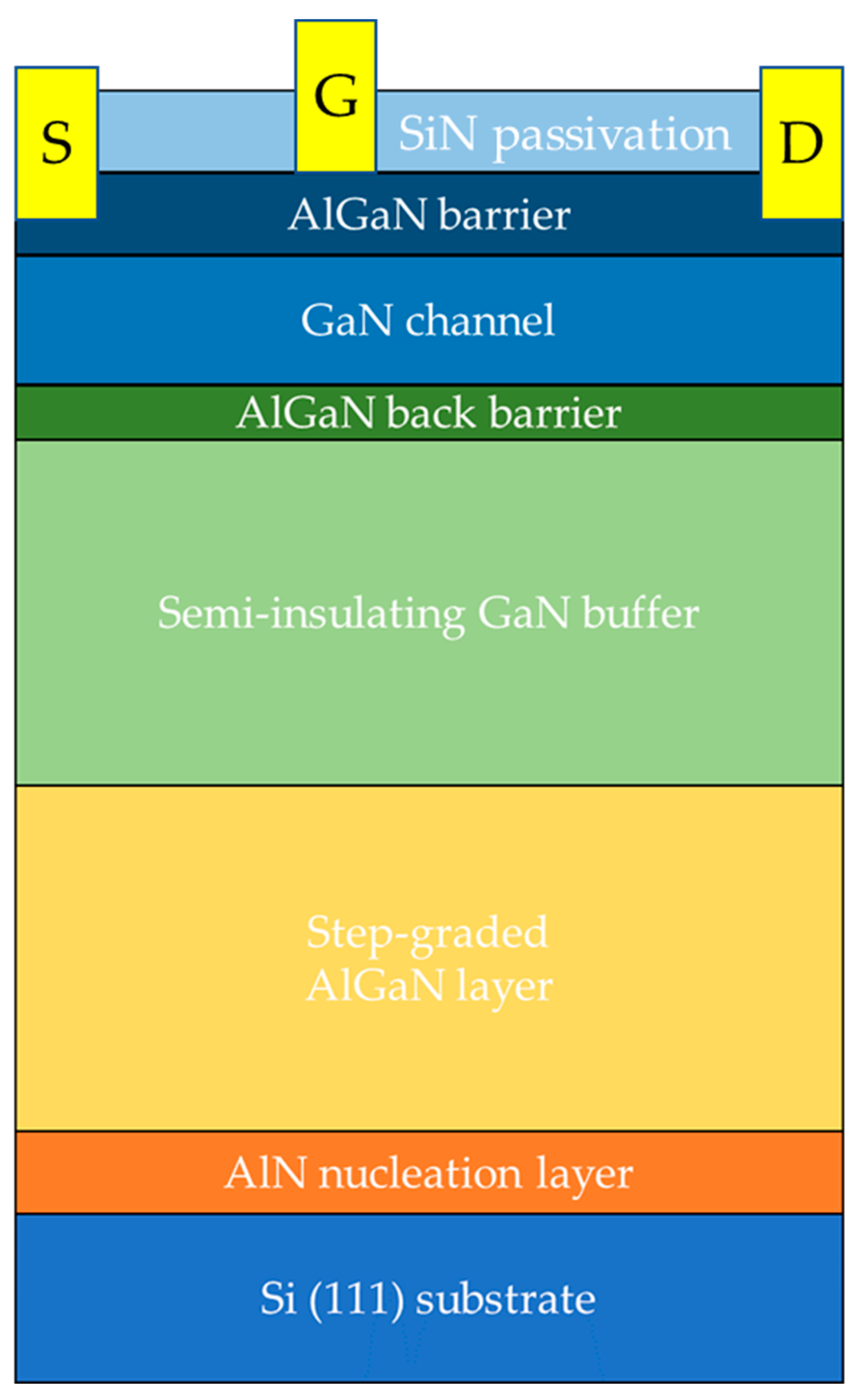
2.1. Growth of AlGaN/GaN Heterostructure Structure

An AlGaN/GaN HEMTs structure on Si was grown on 2-inch Si (111) substrate by metalorganic chemical vapor deposition (MOCVD). Prior to the growth of the epitaxial layers, the Si (111) substrate was chemically cleaned by using diluted HF (DHF) to effectively eliminate the native oxide. For the precursors of MOCVD, Trimethylgallium (TMGa), trimethylaluminum (TMAl) and ammonia (NH3) were used as the sources of Ga, Al and N, respectively, and H2 was the carrier gas.
Firstly, to prevent the Si-Ga melt-back etching, an AlN nucleation layer was grown on the Si (111) substrate. The thickness of the AlN nucleation layer strongly affects the growth of upper epitaxial layers; thus, it is essential to optimize the thickness of the AlN nucleation layer. After that, thick step-graded AlGaN buffer layers were grown on the AlN nucleation layer with different Al compositions and thicknesses of the AlGaN layer. On the optimized step-graded AlGaN buffer layer, a periodical C-doped GaN buffer layer of 2 μm was grown as the semi-insulating buffer layer. This distinct layer has much better crystal quality with semi-insulating characteristics than a conventional C-doped GaN buffer layer, proved by our previous research [21].
After that, the AlGaN back barrier layer was inserted between the semi-insulating C-doped GaN buffer layer and GaN channel layer to improve the carrier confinement in the 2-DEG channel and reduce buffer trapping effects. The AlGaN back barrier layer prevents the transfer of electrons in the GaN channel layer to the buffer layer, resulting in reduced leakage current and improved breakdown voltage. In addition, the dislocations from the buffer layers can be effectively blocked by the back barrier, and, hence, the quality of the GaN channel layer is going to be enhanced.
Sequentially, the AlGaN/GaN heterostructure composed of an unintentionally doped GaN channel layer with a thickness of 100 nm and a 25 nm thick AlGaN barrier with Al composition of 25% were grown at a growth temperature of 1070 °C.
Prior to device fabrication, the 2-DEG property of the optimized epitaxial structure was estimated by Hall measurements using the Van der Pauw method such as electron density of 8.91 × 1012 cm−2, electron mobility of 1600 cm2/V·s and sheet resistance of 429.9 ohm/sq, as shown in Table 1. In addition, the RMS roughness of the AlGaN/GaN heterostructure was 0.462 nm, measured by Atomic Force Microscope (AFM), as shown in Figure 1.

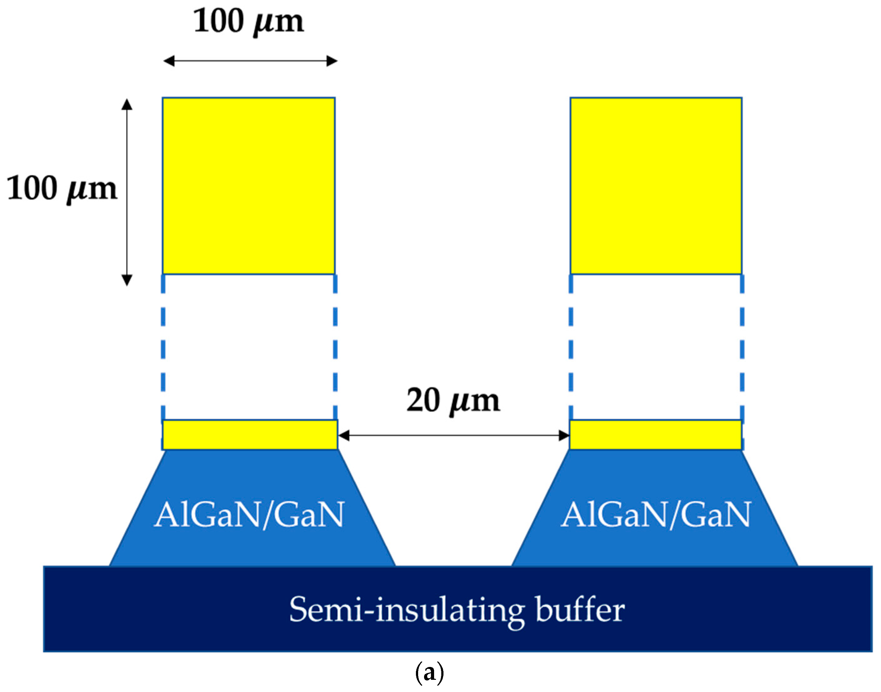
2.2. Device Fabrication

As shown in Figure 2, an AlGaN/GaN HEMT was fabricated on the Si (111) substrate. Firstly, MESA isolation was performed by using Cl2/Ar gases in an inductively coupled plasma-reactive ion etcher (ICP-RIE) for the device isolation. The depth of etching was 300 nm, almost two times larger than the total thickness of the AlGaN/GaN heterostructure, for certain device isolation. For the source/drain ohmic contact, an Si/Ti/Al/Ni/Au (1/25/160/40/100 nm) metal stack was formed by e-beam evaporator, and 2-step rapid thermal annealing (RTA) at 500 °C for 20 s and 850 °C for 30 s in ambient N2 was sequentially performed [22]. For the better ohmic contact, the AlGaN barrier was partially recessed where 5 nm remained of the AlGaN barrier [23]. The contact resistance was 0.63 ohm∙mm, evaluated by the transfer length method (TLM). Finally, for the gate electrode, Ni/Au (50/150 nm) was deposited by e-beam evaporator with a sufficiently high work function of 5.1 eV to have Schottky contact. Finally, the SiN passivation layer was deposited by PECVD, and the device had a gate length (LG) of 3 μm, gate width (WG) of 50 μm and gate–drain distance (LGD) of 10 μm.

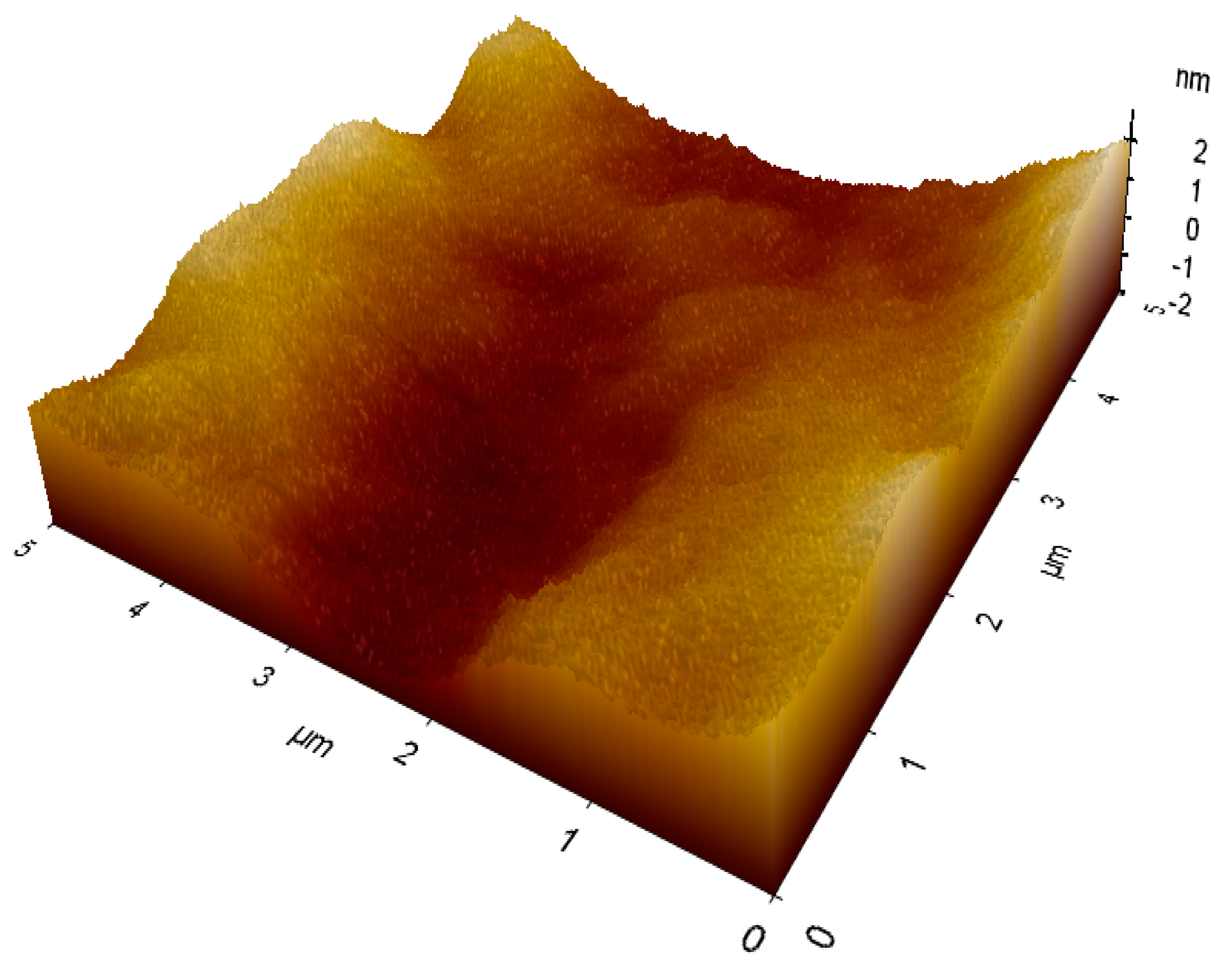
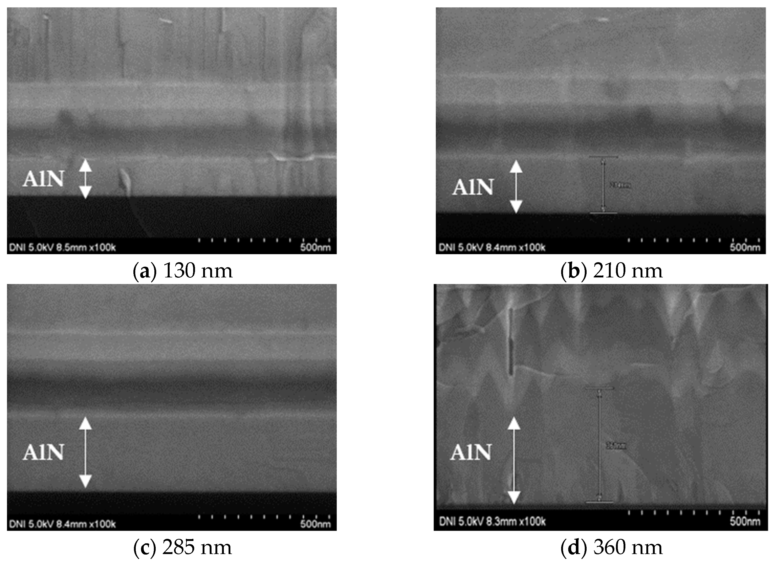
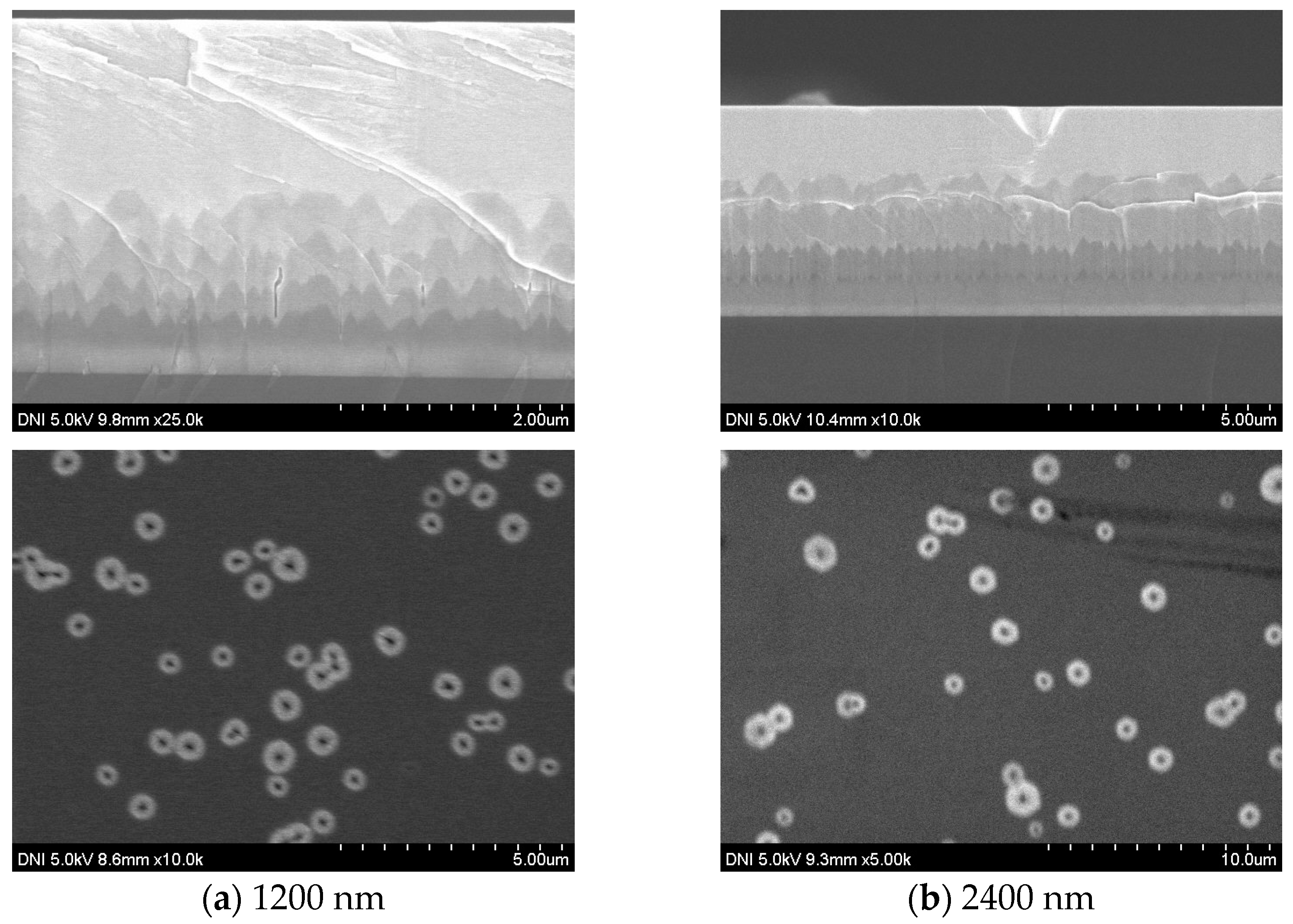
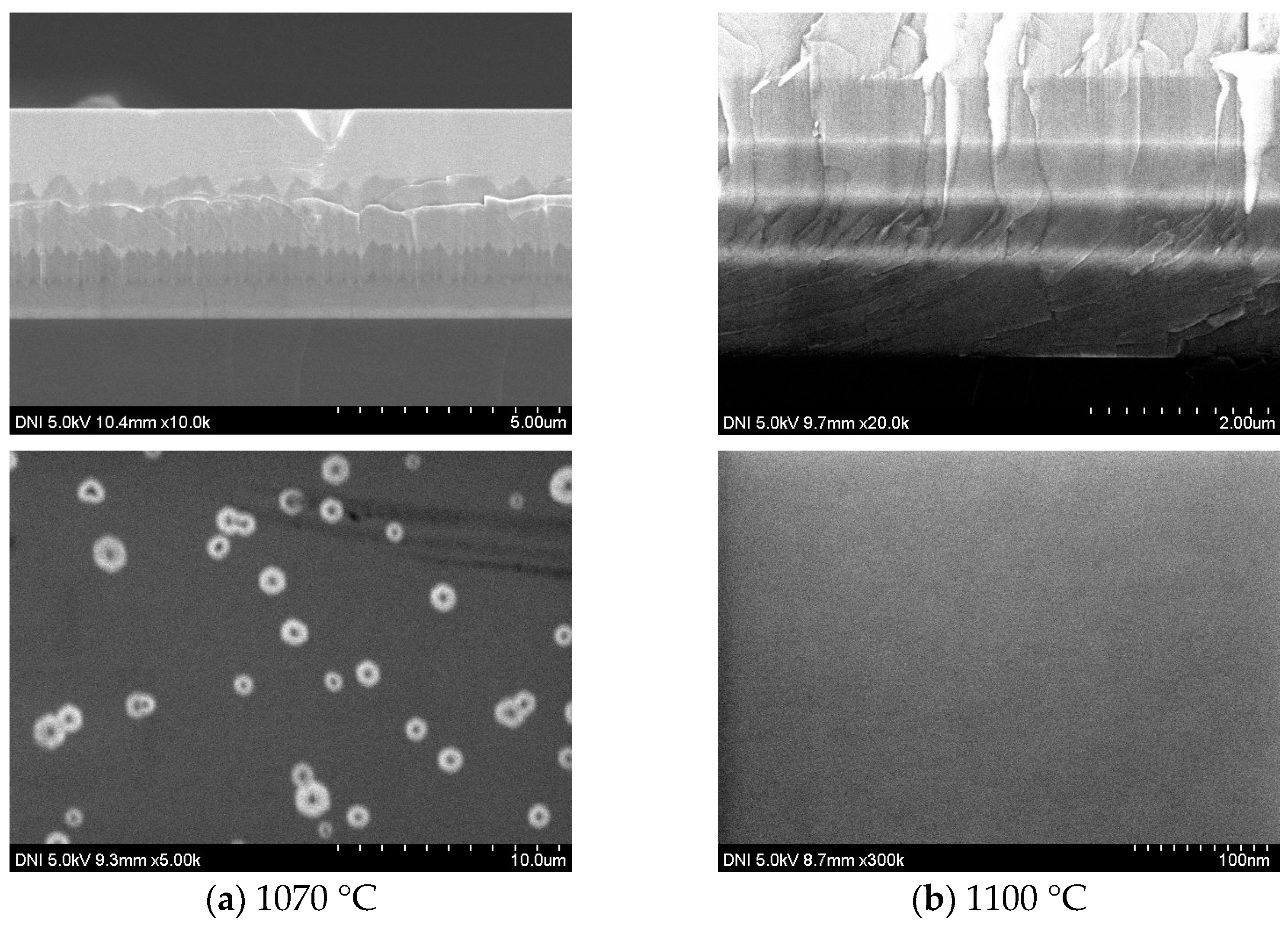
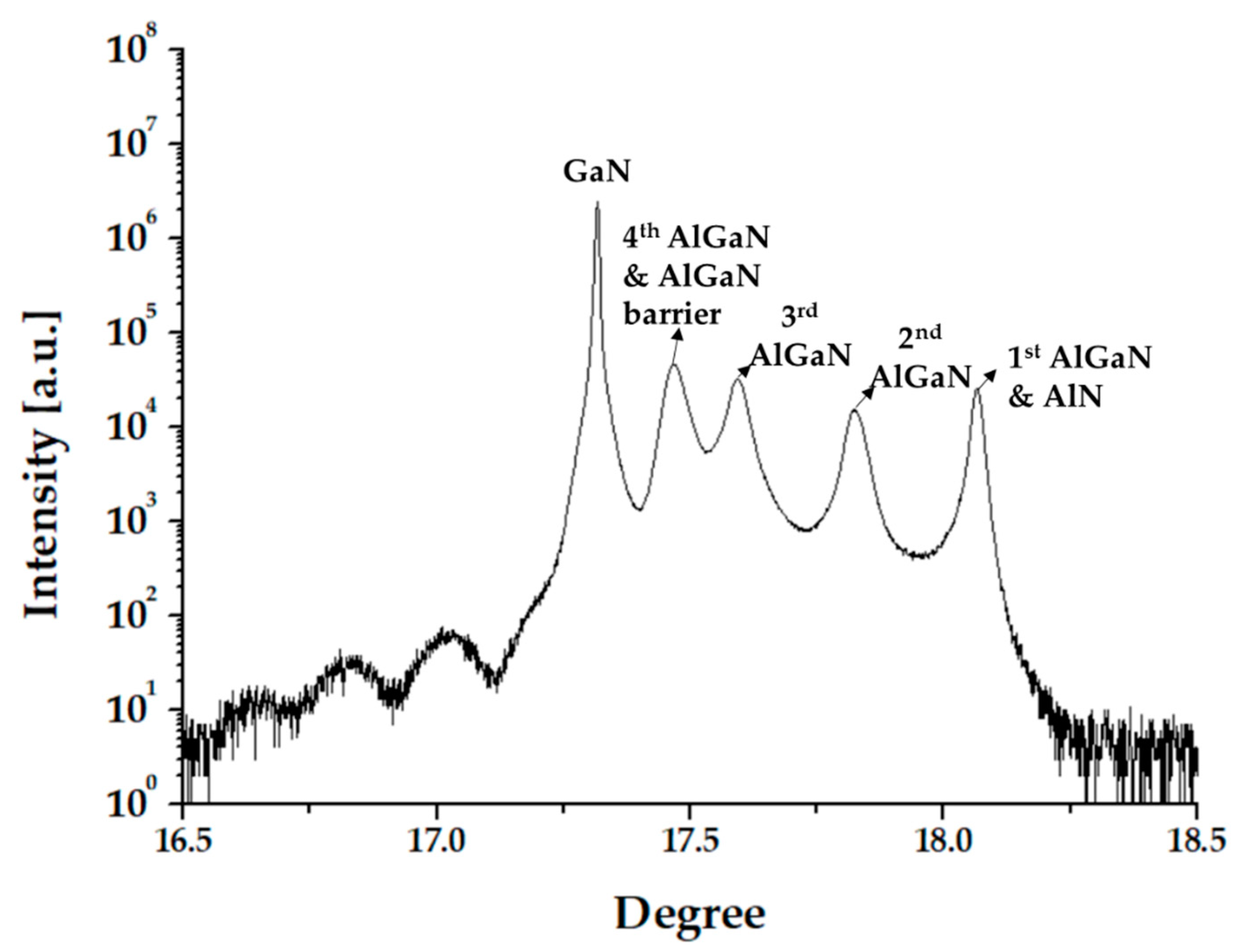
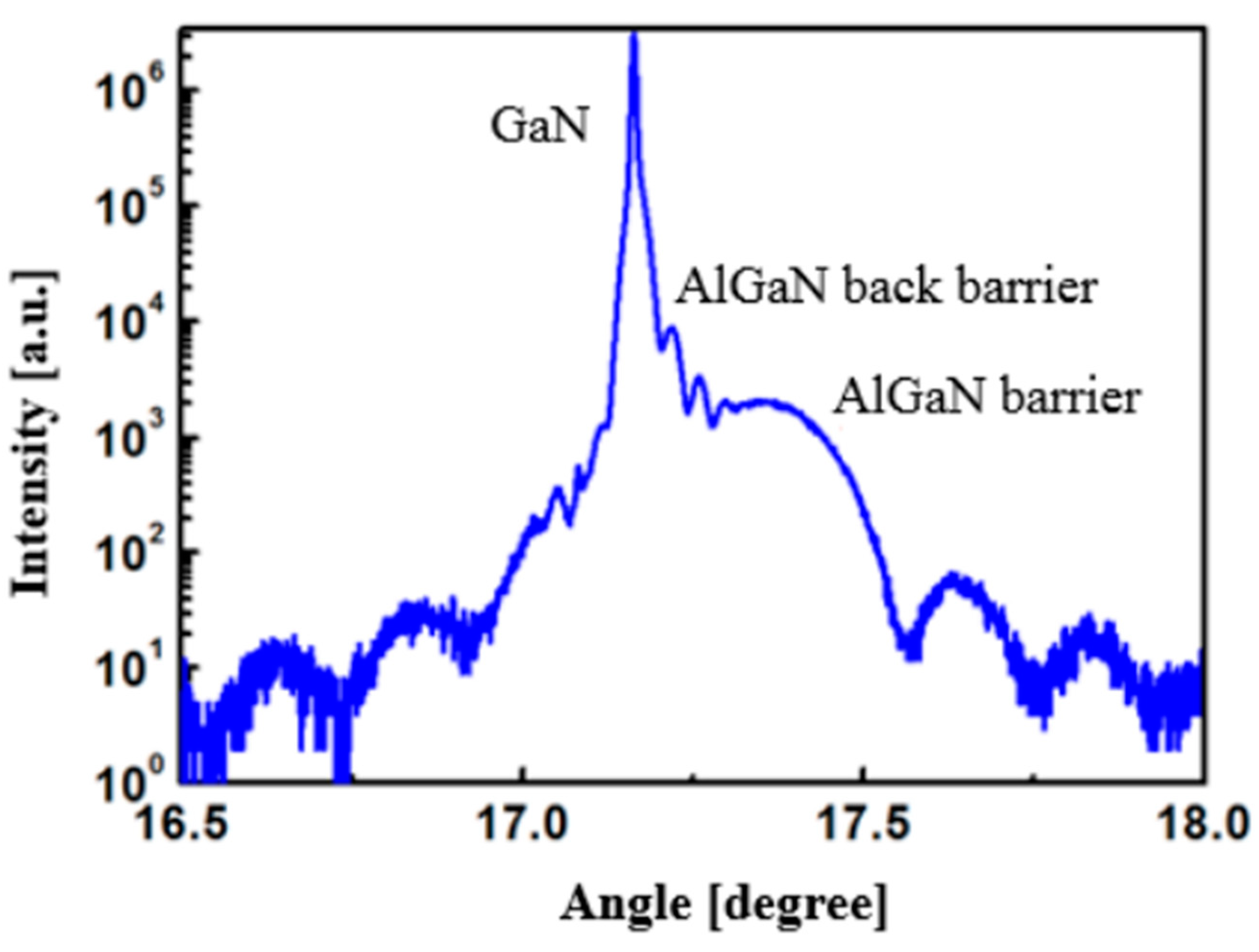
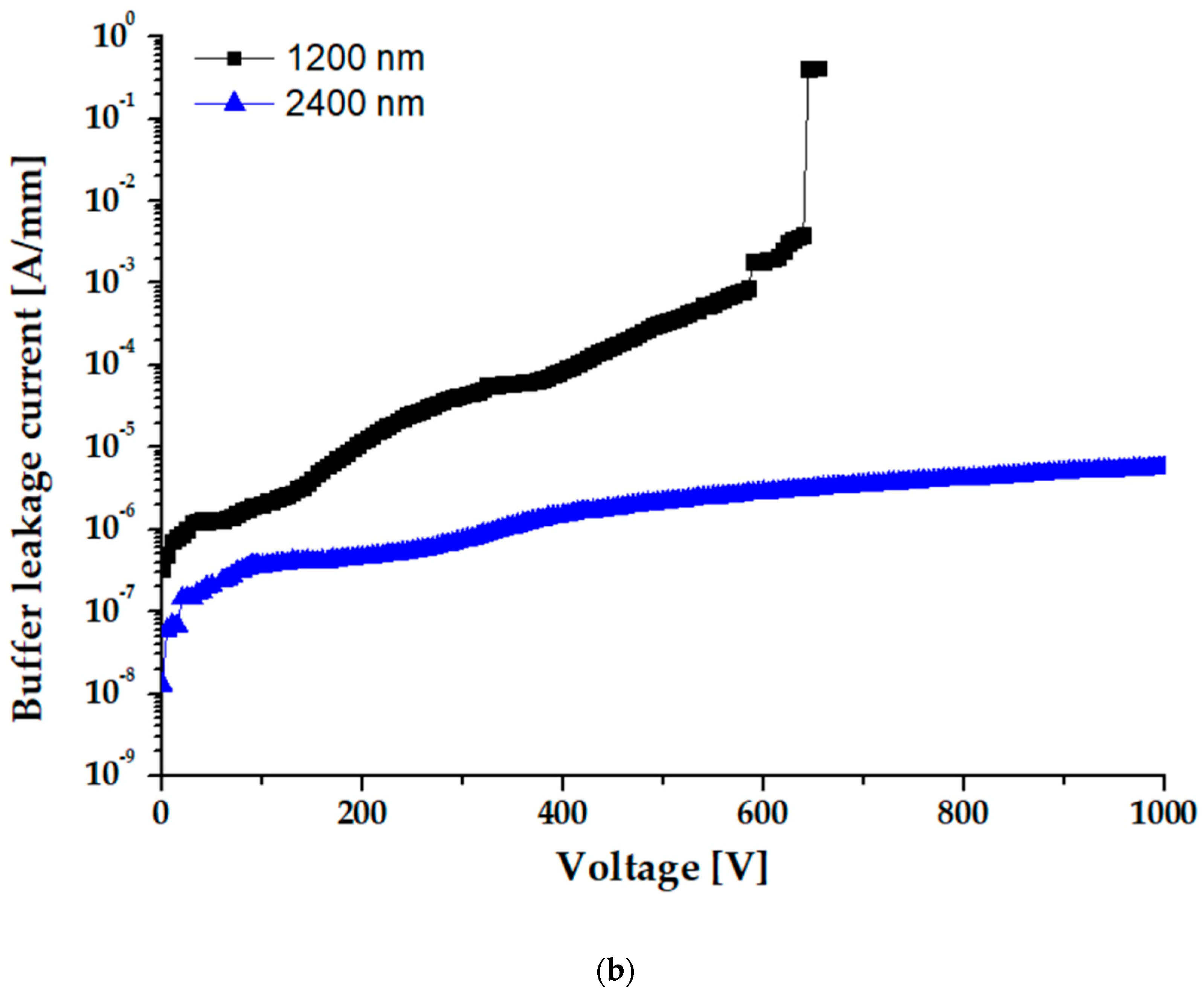
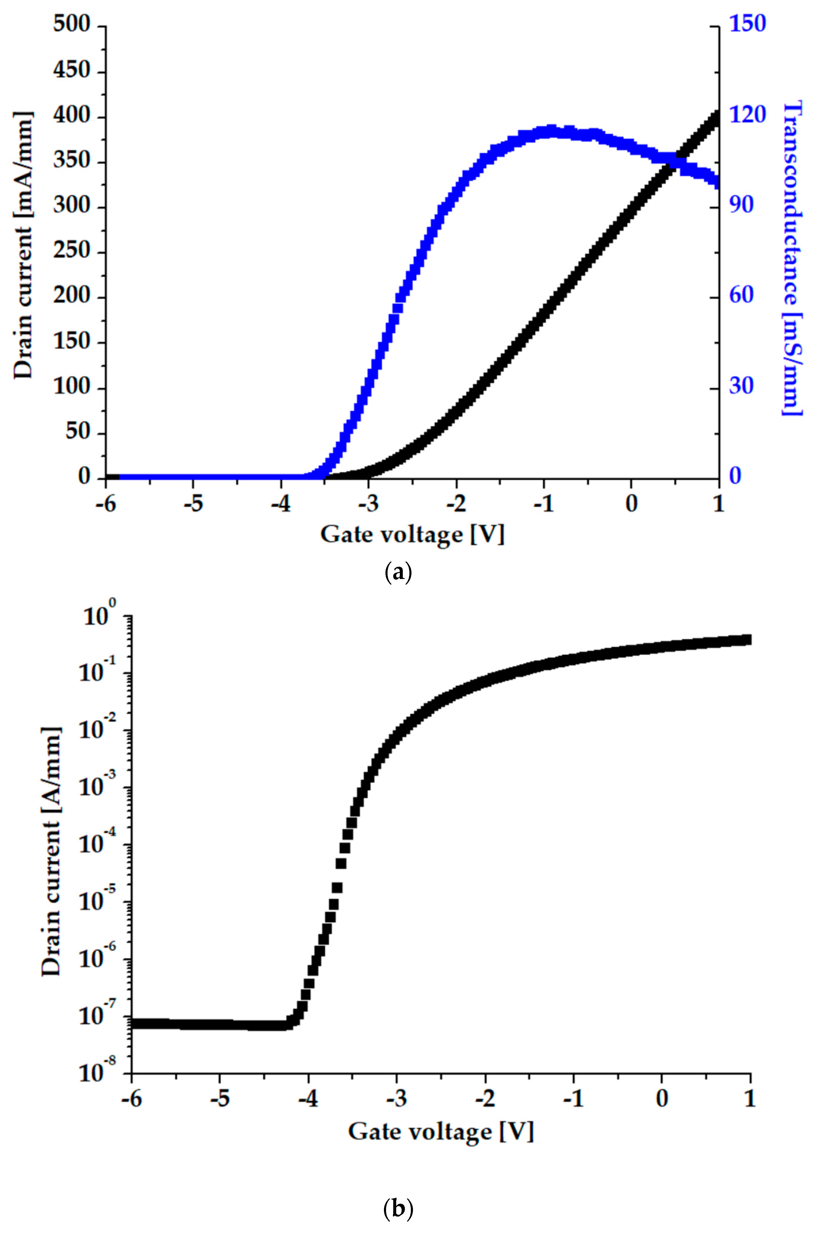
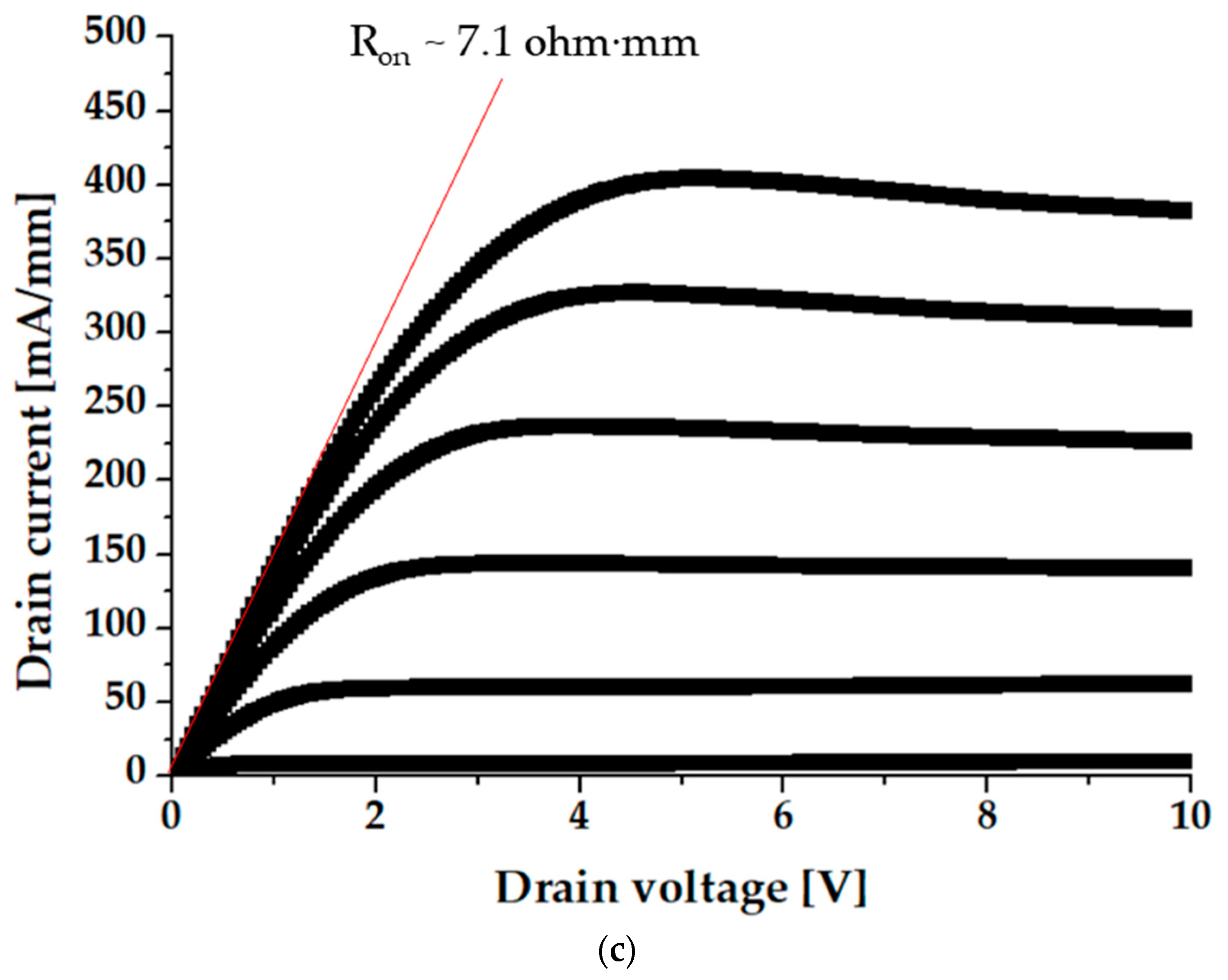
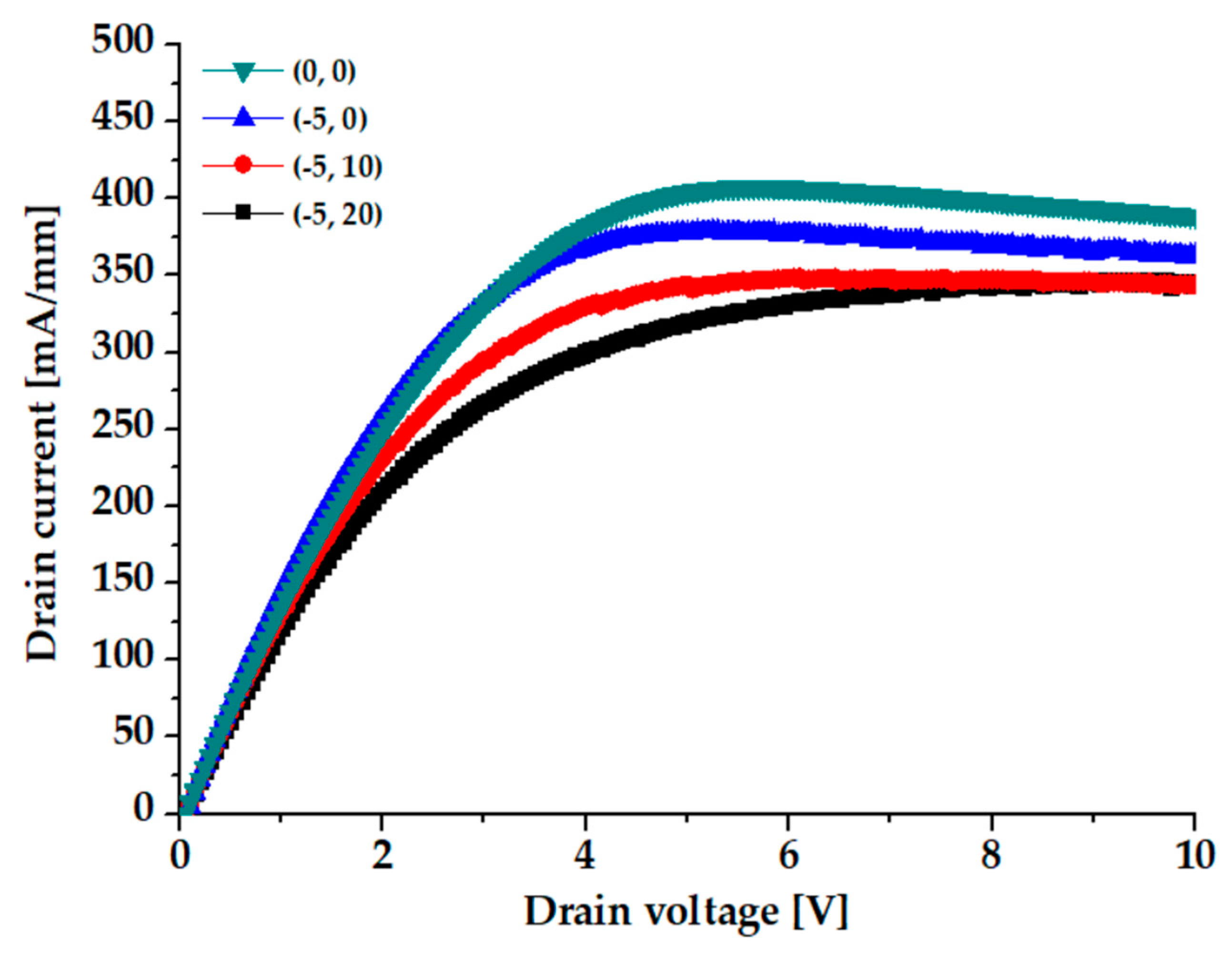
3. Results and Discussion

Firstly, to obtain a crack-free epitaxial structure, an AlN nucleation layer was grown on the Si (111) substrate at a growth temperature of 1100 °C. The thickness of the AlN layer was split into 130, 210, 285 and 360 nm, respectively, and it was revealed that the thickness of 285 nm had the most favorable cross-section in the SEM image, resulting in a smoother surface. In addition, the AlN nucleation layer should be relatively thick enough to prevent the Si diffusion from the substrate to the GaN layer. However, it is noted that a more than 300 nm thick AlN nucleation layer makes lots of stress and strain, resulting in the degradation of AlN layer roughness, as shown in Figure 3.
After that, thick step-graded AlGaN buffer layers were grown on the AlN nucleation layer, which consists of four different AlGaN layers with different Al composition. The Al composition was gradually decreased from the bottom one to the upper one to reduce the stress in the epitaxial layers. To find the effects of AlGaN layer thickness, two different entire step-graded AlGaN buffer layers of thickness 1200 and 2400 nm were grown. As shown in Figure 4, it was clearly observed that thicker step-graded AlGaN buffer layers of 2400 nm presented a much improved interface and surface. In addition, it is desirable to grow a thick buffer layer to improve the breakdown voltage for the GaN-on-Si HEMTs.
Still, the step-graded AlGaN buffer layer of 2400 nm thickness grown at 1070 °C showed a rough interface and several pits on the surface. It is widely reported that Al adatoms can be more effectively spread out on the surface by increasing the growth temperature. This is because the surface mobility of Al adatoms increases, and, finally, the Al atoms can be more uniformly distributed on the surface, resulting in a better interface and surface roughness. It was obviously confirmed that the step-graded AlGaN buffer layer grown at the higher temperature of 1100 °C had greatly enhanced interface and surface quality without a crack, as shown in Figure 5b. The Al composition in each step-graded AlGaN layer was measured by X-ray diffraction (XRD) omega-2theta scan as shown in Figure 6. The Al composition from the undermost layer to uppermost layer was gradually increased from 23.8% to 95.0%, and the thickness of each AlGaN layer is described in Table 2. It is believed that this gradual change in Al composition can effectively reduce the strain and stress in the epitaxial layers.
To find the optimum growth conditions, the AlGaN back barrier was grown on the sapphire substrate because the step-graded AlGaN buffer layer and the back barrier peaks are overlapped on silicon substrate. The thickness of the back barrier and composition of Al are very critical for improving the epitaxial quality. Firstly, to find the optimum thickness of the back barrier, the thickness was varied from 30 to 50 nm. Theoretically, it is desirable to have a thicker back barrier so that it can improve the carrier confinement. However, the epitaxial stress will become larger with a thick back barrier, inducing the degradation of 2-DEG characteristics such as electron mobility and sheet resistance. The 2-DEG property with a 30 nm thick AlGaN back barrier layer was better than that of the 40 and 50 nm thick AlGaN back barriers, such as a 5% improved sheet resistance and 2% improved electron mobility.
After that, the Al composition in the back barrier was increased from 5 to 11% because a less than 5% Al composition is too small to have better carrier confinement with the optimized thickness of 30 nm. To increase the Al composition in the AlGaN back barrier, TMAl flow was increased in MOCVD. It was observed that the 2-DEG property was gradually degraded with increasing Al composition from 7 to 9 to 11%. It is believed that the larger lattice mismatch and stress applied to the epitaxial structure induced the deterioration of the epitaxial quality. In conclusion, the 30 nm thickness and Al composition of 5% are the most suitable conditions for a high-quality AlGaN back barrier, as shown in Figure 7.
To confirm the semi-insulating characteristics, the buffer leakage current was evaluated with the isolated pattern as shown in Figure 8a. The size of the metal was 100 μm × 100 μm, and the distance between each pattern was 20 μm. As shown in Figure 8b, the buffer leakage with the thicker buffer of 2400 nm still remained with a low current level of 10−6 A/mm even at 1000 V; however, the breakdown occurred with the thinner buffer layer around 630 V. It is clearly indicated that the thick buffer layer is highly desirable for the high-power device, and the device with the 2400 nm thick step-graded AlGaN buffer layer still survives even at 1000 V.
Figure 9a,b show the transfer characteristics(ID-VG) of the device at the saturation region (VDS = 10 V) with optimized epitaxial structure. The threshold voltage (Vth) of −2.83 V was extracted by the linear extrapolation method. The AlGaN/GaN HEMT exhibited a drain current of 403 mA/mm at the gate voltage of 1 V and maximum transconductance of 116 mS/mm with a very low off-state leakage current of ~7 × 10⁻⁸ A/mm and high on/off current ratio of ~107, resulting from the enhancement of carrier confinement by introducing the AlGaN back barrier. The output characteristics of AlGaN/GaN HEMTs were assessed with the variation of gate voltage from –6 V to 1 V as shown in Figure 9c. The relatively low RON of 7.1 ohm∙mm was extracted at a current level of 200 mA/mm. The optimized buffer structure and back barrier structure make these enhanced device characteristics.
The pulsed I–V characteristics were analyzed at a gate voltage of 1 V under the electrical stress condition of a pulse width of 50 μs and a period of 1 ms to evaluate the trapping effects, as shown in Figure 10. The stress conditions were varied from the cold quiescent bias point (Vgs = Vds = 0 V) to the pinch-off condition (Vgs = Vds = –5 V) called gate lag and, finally, to the drain lag condition with the increase in drain stress bias from 0 to 20 V. The device indicated outstanding performance with a very low current dispersion of 6.5% under the bias stress of (–5, 0). Even under the stress condition of (–5, 20), the device achieved an excellent current dispersion of 11.2% compared to other research results [24,25], indicating that the optimized buffer structure and AlGaN back barrier remarkably suppress buffer trapping effects.

4. Conclusions

We have grown a crack-free AlGaN/GaN heterostructure on Si (111) substrate with an optimized AlN nucleation layer, step-graded AlGaN buffer layer and AlGaN back barrier by varying the thicknesses and material compositions in the layers, which is very crucial to GaN-based epitaxial layers for power applications. With those optimized epitaxial structures, the device characteristics of AlGaN/GaN HEMTs on Si (111) substrate were investigated. The devices showed a drain current of 403 mA/mm and a transconductance of 116 mS/mm with a high on/off current ratio (Ion/Ioff) of ~107, indicating that the optimized buffer structure including AlGaN back barrier successfully blocked the carrier moving from channel to buffer layer. Furthermore, it is confirmed that the trapping effect was also greatly suppressed with the optimized crack-free AlGaN/GaN heterostructure.

Funding

This work was supported by the Dong-A University research fund.

Institutional Review Board Statement

Not applicable.

Informed Consent Statement

Not applicable.

Data Availability Statement

Data are contained within the article.

Conflicts of Interest

The author declares no conflict of interest.

References

  1. Wei, J.; Tang, G.; Xie, R.; Chen, K.J. GaN Power IC Technology on P-GaN Gate HEMT Platform. Jpn. J. Appl. Phys. 2020, 59, SG0801. [Google Scholar] [CrossRef]
  2. Zhang, N.-Q.; Keller, S.; Parish, G.; Heikman, S.; DenBaars, S.P.; Mishra, U.K. High Breakdown GaN HEMT with Overlapping Gate Structure. IEEE Electron. Device Lett. 2000, 21, 421–423. [Google Scholar] [CrossRef]
  3. Fujita, S. Wide-Bandgap Semiconductor Materials: For Their Full Bloom†. Jpn. J. Appl. Phys. 2015, 54, 30101. [Google Scholar] [CrossRef]
  4. Chen, K.J.; Häberlen, O.; Lidow, A.; Tsai, C.L.; Ueda, T.; Uemoto, Y.; Wu, Y. GaN-on-Si Power Technology: Devices and Applications. IEEE Trans. Electron Devices 2017, 64, 779–795. [Google Scholar] [CrossRef]
  5. Ishikawa, H.; Zhao, G.-Y.; Nakada, N.; Egawa, T.; Jimbo, T.; Umeno, M. GaN-on-Si Substrate with AlGaN/AlN Intermediate Layer. Jpn. J. Appl. Phys. 1999, 38, L492. [Google Scholar] [CrossRef]
  6. Marcon, D.; Saripalli, Y.N.; Decoutere, S. 200mm GaN-on-Si Epitaxy and e-Mode Device Technology. In Proceedings of the 2015 IEEE International Electron Devices Meeting (IEDM), Washington, DC, USA, 7–9 December 2015; pp. 16.2.1–16.2.4. [Google Scholar]
  7. Luo, W.; Wang, X.; Guo, L.; Xiao, H.; Wang, C.; Ran, J.; Li, J.; Li, J. Influence of AlN Buffer Layer Thickness on the Properties of GaN Epilayer on Si(111) by MOCVD. Microelectron. J. 2008, 39, 1710–1713. [Google Scholar] [CrossRef]
  8. Zhao, S.-X.; Liu, X.-Y.; Zhang, L.-Q.; Huang, H.-F.; Shi, J.-S.; Wang, P.-F. Impacts of Thermal Atomic Layer-Deposited AlN Passivation Layer on GaN-on-Si High Electron Mobility Transistors. Nanoscale Res. Lett. 2016, 11, 137. [Google Scholar] [CrossRef] [PubMed]
  9. Huang, S.; Jiang, Q.; Yang, S.; Zhou, C.; Chen, K.J. Effective Passivation of AlGaN/GaN HEMTs by ALD-Grown AlN Thin Film. IEEE Electron. Device Lett. 2012, 33, 516–518. [Google Scholar] [CrossRef]
  10. Kim, H.; Schuette, M.L.; Lee, J.; Lu, W.; Mabon, J.C. Passivation of Surface and Interface States in AlGaN/GaN HEMT Structures by Annealing. J. Electron. Mater. 2007, 36, 1149–1155. [Google Scholar] [CrossRef]
  11. Tzou, A.-J.; Chu, K.-H.; Lin, I.-F.; Østreng, E.; Fang, Y.-S.; Wu, X.-P.; Wu, B.-W.; Shen, C.-H.; Shieh, J.-M.; Yeh, W.-K.; et al. AlN Surface Passivation of GaN-Based High Electron Mobility Transistors by Plasma-Enhanced Atomic Layer Deposition. Nanoscale Res. Lett. 2017, 12, 315. [Google Scholar] [CrossRef] [PubMed]
  12. Wienecke, S.; Romanczyk, B.; Guidry, M.; Li, H.; Zheng, X.; Ahmadi, E.; Hestroffer, K.; Megalini, L.; Keller, S.; Mishra, U.K. N-Polar Deep Recess MISHEMTs With Record 2.9 W/Mm at 94 GHz. IEEE Electron. Device Lett. 2016, 37, 713–716. [Google Scholar] [CrossRef]
  13. Li, W.; Romanczyk, B.; Guidry, M.; Akso, E.; Hatui, N.; Wurm, C.; Liu, W.; Shrestha, P.; Collins, H.; Clymore, C.; et al. Record RF Power Performance at 94 GHz From Millimeter-Wave N-Polar GaN-on-Sapphire Deep-Recess HEMTs. IEEE Trans. Electron. Devices 2023, 70, 2075–2080. [Google Scholar] [CrossRef]
  14. Akso, E.; Collins, H.; Clymore, C.; Li, W.; Guidry, M.; Romanczyk, B.; Wurm, C.; Liu, W.; Hatui, N.; Hamwey, R.; et al. First Demonstration of Four-Finger N-Polar GaN HEMT Exhibiting Record 712-MW Output Power With 31.7% PAE at 94 GHz. IEEE Microw. Wirel. Technol. Lett. 2023, 33, 683–686. [Google Scholar] [CrossRef]
  15. Moon, J.; Wong, J.; Grabar, B.; Antcliffe, M.; Chen, P.; Arkun, E.; Khalaf, I.; Corrion, A. High-Speed Linear GaN Technology with a Record Efficiency in Ka-Band. In Proceedings of the 2019 14th European Microwave Integrated Circuits Conference (EuMIC), Paris, France, 30 September–1 October 2019; pp. 57–59. [Google Scholar]
  16. Moon, J.S.; Wu, S.; Wong, D.; Milosavljevic, I.; Conway, A.; Hashimoto, P.; Hu, M.; Antcliffe, M.; Micovic, M. Gate-Recessed AlGaN-GaN HEMTs for High-Performance Millimeter-Wave Applications. IEEE Electron. Device Lett. 2005, 26, 348–350. [Google Scholar] [CrossRef]
  17. Moon, J.-S.; Grabar, B.; Wong, J.; Dao, C.; Arkun, E.; Tai, H.; Fanning, D.; Miller, N.C.; Elliott, M.; Gilbert, R.; et al. W-Band Graded-Channel GaN HEMTs with Record 45% Power-Added-Efficiency at 94 GHz. IEEE Microw. Wirel. Technol. Lett. 2023, 33, 161–164. [Google Scholar] [CrossRef]
  18. Harrouche, K.; Kabouche, R.; Okada, E.; Medjdoub, F. High Power AlN/GaN HEMTs with Record Power-Added-Efficiency >70% at 40 GHz. In Proceedings of the 2020 IEEE/MTT-S International Microwave Symposium (IMS), Los Angeles, CA, USA, 4–6 August 2020; pp. 285–288. [Google Scholar]
  19. Shanbhag, A.; Sruthi, M.P.; Medjdoub, F.; Chakravorty, A.; DasGupta, N.; DasGupta, A. Optimized Buffer Stack with Carbon-Doping for Performance Improvement of GaN HEMTs. In Proceedings of the 2021 IEEE BiCMOS and Compound Semiconductor Integrated Circuits and Technology Symposium (BCICTS), Monterey, CA, USA, 5–8 December 2021; pp. 1–4. [Google Scholar]
  20. Harrouche, K.; Kabouche, R.; Okada, E.; Medjdoub, F. High Performance and Highly Robust AlN/GaN HEMTs for Millimeter-Wave Operation. IEEE J. Electron. Devices Soc. 2019, 7, 1145–1150. [Google Scholar] [CrossRef]
  21. Kang, H.-S.; Kim, D.-S.; Won, C.-H.; Kim, Y.-J.; Yoon, Y.J.; Kim, D.-K.; Lee, J.-H.; Bae, Y.; Cristoloveanu, S. Impact of Multi-Layer Carbon-Doped/Undoped GaN Buffer on Suppression of Current Collapse in AlGaN/GaN HFETs. Int. J. High Speed Electron. Syst. 2014, 23, 1450017. [Google Scholar] [CrossRef]
  22. Desmaris, V.; Eriksson, J.; Rorsman, N.; Zirath, H. Low-Resistance Si/Ti/Al/Ni/Au Multilayer Ohmic Contact to Undoped AlGaN/GaN Heterostructures. Electrochem. Solid-State Lett. 2004, 7, G72. [Google Scholar] [CrossRef]
  23. Lau, W.S.; Tan, J.B.H.; Singh, B.P. Formation of Ohmic contacts in AlGaN/GaN HEMT structures at 500°C by Ohmic contact recess etching. Microelectron. Reliab. 2009, 49, 558–561. [Google Scholar] [CrossRef]
  24. Subramani, N.K. Physics-Based TCAD Device Simulations and Measurements of GaN HEMT Technology for RF Power Amplifier Applications. Doctoral Dissertation, Université de Limoges, Limoges, Limoges, 2017. [Google Scholar]
  25. Omika, K.; Tateno, Y.; Kouchi, T.; Komatani, T.; Yaegassi, S.; Yui, K.; Nakata, K.; Nagamura, N.; Kotsugi, M.; Horiba, K.; et al. Operation Mechanism of GaN-based Transistors Elucidated by Element-Specific X-ray Nanospectroscopy. Sci. Rep. 2018, 8, 13268. [Google Scholar] [CrossRef] [PubMed]
Figure 1. RMS roughness of AlGaN/GaN heterostructure on Si (111) by AFM.
Coatings 14 00700 g001
Figure 2. Schematic of AlGaN/GaN HEMT on Si epitaxial structure.
Coatings 14 00700 g002
Figure 3. Cross-sectional SEM image of AlN nucleation layer with various thicknesses.
Coatings 14 00700 g003
Figure 4. Cross-sectional and surface SEM image of step-graded AlGaN layers with different thicknesses of AlGaN layers: (a) 1200 nm, (b) 2400 nm.
Coatings 14 00700 g004
Figure 5. Cross-sectional and surface SEM image of step-graded AlGaN layers grown at the different growth temperatures: (a) 1070 °C, (b) 1100 °C.
Coatings 14 00700 g005
Figure 6. X-ray diffraction (XRD) omega-2theta scan of step-graded AlGaN buffer layer.
Coatings 14 00700 g006
Figure 7. X-ray diffraction (XRD) omega-2theta scan of AlGaN back barrier layer.
Coatings 14 00700 g007
Figure 8. (a) Isolated device pattern and (b) characteristics of buffer leakage current with different step-graded AlGaN layer thicknesses of 1200 and 2400 nm.
Coatings 14 00700 g008aCoatings 14 00700 g008b
Figure 9. Comparison of AlGaN/GaN HEMTs in terms of transfer characteristics: (a) linear scale and (b) log scal, (c)output characteristics.
Coatings 14 00700 g009aCoatings 14 00700 g009b
Figure 10. Pulsed I–V characteristics of AlGaN/GaN HEMTs under the stress conditions of (0, 0), (−5, 0), (−5, 10) and (−5, 20).
Coatings 14 00700 g010
Table 1. 2-DEG property of AlGaN/GaN heterostructure with optimized buffer structure.
2-DEG Property
Electron Desity [cm−2]Electron Mobility [cm2/V·s]Sheet Resistance [ohm/sq]
8.91 × 10121600429.9
Table 2. Al composition and thickness of the optimized step-graded AlGaN buffer layer.
PositionAl Composition [%]Thickness [nm]
1st AlGaN layer95.0651
2nd AlGaN layer78.1582
3rd AlGaN layer42.7563
4th AlGaN layer23.8637
Disclaimer/Publisher’s Note: The statements, opinions and data contained in all publications are solely those of the individual author(s) and contributor(s) and not of MDPI and/or the editor(s). MDPI and/or the editor(s) disclaim responsibility for any injury to people or property resulting from any ideas, methods, instructions or products referred to in the content.

