Abstract
In this paper, we study the nonlinear optical bistability (OB) in a symmetrical multilayer structure. This multilayer structure is constructed by embedding a nonlinear three-dimensional Dirac semimetal (3D DSM) into a Fabry–Perot cavity composed of one-dimensional photonic crystals. The OB phenomenon stems from the third order nonlinear conductivity of 3D DSM. The local field of resonance mode could enhance the nonlinearity and reduce the thresholds of OB. This structure achieves the tunability of OB due to the fact that the transmittance could be modulated by the Fermi energy. It is found that the OB threshold and threshold width could be remarkably reduced by increasing the Fermi energy of the 3D DSM. Besides, we also found that the OB curve depends heavily on the angle of incidence of the incident light, the structural parameters of the Fabry–Perot cavity, and the position of the 3D DSM inside the cavity. After parameter optimization, we obtained OB with a threshold of . We believe this simple multilayer structure could provide a reference idea for realizing low-threshold and tunable all-optical switching devices.
1. Introduction
Optical bistability (OB) is a typical optical phenomenon, which refers to the nonlinear optical phenomenon where an input light intensity corresponds to two output light intensities that can be converted into each other within a certain range, and at this time, there is a hysteresis loop similar to the “S” shape between the input and output light intensities [1,2]. Due to the nonlinear characteristics similar to the hysteresis curve, OB has been widely used in fields such as optical communication and photonic computing, biosensors [3], all-optical switching [4], optical transistors [5], and optical memories [6]. Currently, the main goal of studying OB is to reduce the threshold of OB to achieve practical OB devices. Generally, researchers’ methods to reduce the OB threshold can be classified into two rough categories: the first category is to take advantage of resonant structures such as photonic crystal micro-cavities [7], Fabry–Perot (FP) cavities [8], fiber Bragg grating cavities [9], and surface plasmon resonance [10,11] to lower the OB threshold by achieving localized field enhancement effect; the second category is to use nonlinear materials with high nonlinear coefficients and add them to micro-nano structures to enhance the nonlinear effect of the system and achieve the goal of reducing the OB threshold. For example, a novel bistable resonator-free all-optical waveguide device based on indium tin oxide as nonlinear epsilon-near-zero material has been reported [12]. In addition, studies have shown that graphene has superior optoelectronic properties and can fully utilize its advantages in the field of OB, with its most prominent feature being its great nonlinear properties. Furthermore, graphene has characteristics such as tunable conductivity and ultra-fast modulation speed, making it a favorite of researchers [13,14]. Currently, researchers are eagerly reporting on the method of reducing the threshold of OB by adding graphene to composite structures [15,16,17]. However, optical bistability schemes based on graphene micro/nanostructures also face many challenges in practical preparation. Recently, people have turned their attention to another type of bulk material similar to graphene, namely three-dimensional Dirac semimetal (3D DSM). Three-dimensional DSM is a bulk medium, and its volume electrons form a three-dimensional Dirac cone, which is also known as “three-dimensional graphene”. Although 3D DSM is called “three-dimensional graphene”, unlike the two-dimensional Dirac fermions on the surface of graphene, 3D DSM has three-dimensional Dirac fermions in the volume. The unique electronic structure of 3D DSM gives it many peculiar properties. Previous reports have shown that 3D DSM not only has similar properties to graphene in controlling the dielectric constant by adjusting the Fermi energy but also exhibits high electron mobility [18], good stability, strong coupling with light, and the ability to avoid the huge metal losses that occur in traditional metal metamaterials [19]. It is worth noting that the nonlinear refractive index coefficient of 3D DSM in the terahertz range is relatively high [20]. Therefore, we observe that the OB phenomenon can be observed at lower incident electric field ranges. Based on these advantages, 3D DSM stands out as a candidate material for constructing nonlinear optical devices in the field of OB, providing a new perspective for designing flexible and controllable nonlinear OB devices.
As is well known, the simplest approach for implementing OB is the FP cavity structure, which can create the conditions necessary for the occurrence of OB by filling the cavity with a nonlinear medium. By increasing the intensity of incident light, the refractive index of the nonlinear medium in the FP cavity changes, resulting in a nonlinear bistable relationship between the input and output light intensities. Traditionally, the FP cavity consists of two mirrors. However, with the development of one-dimensional photonic crystals (1D PCs), researchers have found that 1D PCs have potential applications in the field of OB. Therefore, the use of two 1D PCs instead of two mirrors in the traditional FP cavity to achieve OB has attracted widespread attention. Currently, many optical devices based on photonic crystal FP cavity structures have been reported, such as optical absorption, optical filters, and nonlinear effects. Therefore, we imagine what changes would occur in the cavity if we used two 1D PCs instead of the two mirrors in the FP cavity and fill the cavity with 3D DSM. Will the hysteresis phenomenon still occur in such a new FP cavity? And what impact will 3D DSM have on the hysteresis phenomenon? Based on this question, we theoretically propose a photonic crystal FP cavity based on 3D DSM, which is placed at the center of the FP cavity. We found that 3D DSM can provide strong nonlinear effects for the structure, and the unique band structure of 1D PC can increase the flexibility of controlling OB. Moreover, the threshold and hysteresis width of OB can be regulated by tuning parameters such as the Fermi energy of 3D DSM, incident angle, relaxation time, period of 1D PC, length of FP cavity, and position of 3D DSM in the cavity. Therefore, we believe that the photonic crystal FP cavity structure based on 3D DSM has potential applications in the field of nonlinear terahertz devices and nanophotonics, providing a reference for achieving low threshold and tunable OB.
2. Theoretical Model and Method
We consider a FP cavity multilayer structure composed of two symmetric photonic crystals, filled with 3D DSM and pure water, as shown in Figure 1. 3D DSM is a bulk material which not only has linear/nonlinear conductivity characteristic similar to graphene but also is very easy to prepare. Under the current conditions of micro and nano processing technology, the preparation of multilayer structures as shown in Figure 1 is already a very mature means. The 3D DSM is placed in the middle of the cavity, and the medium C is placed on both sides of the 3D DSM. Medium C is pure water with a refractive index of and a thickness of . In fact, if pure water were replaced with an aqueous solution, this structure could also find potential applications in the field of biosensors. We will not delve into this discussion here for now. The photonic crystal is composed of dielectric materials A and B with a cycle of , where the refractive index of dielectric material A is and dielectric material B is glass with a refractive index of [21]. We know that the loss in the actual material has a significant impact on the performance of optical devices. However, for OB, what we are more concerned about is the threshold of the entire structure and the movement of the entire curve in the left and right directions. Therefore, we did not additionally consider material loss in the manuscript. The thicknesses of A and B are and , respectively. The central wavelength is set as , and the cavity length is set to . The thickness of dielectric material A and B is set as , and the thickness of medium C is also set as . The initial parameters of 3D DSM are set as , , and . The direction perpendicular to the photonic crystal is set as the z direction, and the incident electromagnetic wave is assumed to be TE polarization. It should be noted that the technology for preparing such multilayer dielectric structures is relatively mature, and because the 3D DSM is a bulk medium, the technical difficulty in manufacturing is reduced. Overall, it is feasible to apply the structure proposed in this paper in practice.
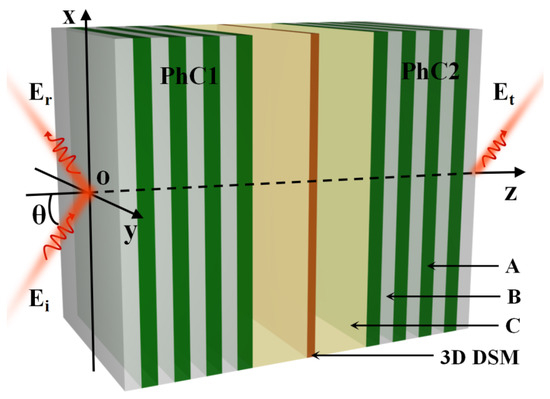
Figure 1.
Schematic diagram of photonic crystal multilayer structure based on 3D DSM.
Ignoring the effects of external magnetic fields and random phase approximation, we can use the semi-classical Boltzmann transport equation with relaxation time approximation to calculate the 3D DSM linear intraband optical conductivity in the terahertz range, as expressed in Equation (1) [22]:
where , is the relaxation time of the 3D DSM, is the Boltzmann constant, is temperature, is the reduced Planck constant, is the Fermi velocity of the electrons, is the polylogarithm function, and is the Fermi energy of the 3D DSM. It should be noted that we ignored the random phase approximation and adopted a simplified model. This is also a commonly used method in many similar works. The calculation of OB here considers the terahertz band. In the terahertz band, there is almost no difference between the linear intraband optical conductivity of 3D DSM under random phase approximation and the approximate model. Besides, the third-order nonlinear optical conductivity of the 3D DSM is expressed as Equation (2) [22]:
On this basis, we can write the third-order polarization of the 3D DSM as the following expression:
where represents the permittivity of vacuum. In addition, the linear complex refractive index of the 3D DSM is denoted as follows:
From the above expressions, it can be found that the third-order polarizability of 3D DSM is bound up with the linear inband optical conductivity , and the linear complex refractive index is bound up with the third-order nonlinear optical conductivity , while regulating the Fermi energy and relaxation time can regulate and . This provides convenient circumstance for effectuating a tunable OB.
The reflectance and transmission of the entire construction is calculated by making use of the transfer matrix method. As shown in Figure 1, we set the light beam to propagate along the z-axis, with the 3D DSM parallel to the x-axis and y-axis, and the 3D DSM is placed at . The transmission matrix of the photonic crystal and the transmission matrix of the aqueous tier inside the cavity can be expressed as follows:
where , is the constituent of medium j disseminating following the z-axis, is the wave vector in vacuum, is the thickness of medium j, is the constituent of the incident wave disseminating follow the y-axis, and is the incident angle.
Then, we canvass the transmission matrix of the nonlinear medium layer, which is the 3D DSM layer in this article. The transmission matrix of a Kerr-type nonlinear material can be expressed as the following equation [23]:
where is the z-component of the forward-propagating wave vector, is the z-component of the backward-propagating wave vector, and their expressions are given by Equation (7):
with , where and are the amplitude of vibration of the forward and backward waves, separately. The wave vectors and can be obtained by disposing of the coupled nonlinear equations below with the aid of the following equation:
where is the transmitted intensity, . If we can calculate a set of coupled nonlinear equations about and through fixed-point iteration, we can obtain the specific expression of the transmission matrix of the 3D DSM layer [24]. First, we set the initial value , and then we seek the stable solutions of and through multiple iterations. Once the solution of is determined, we can calculate the transmission matrix of the 3D DSM layer using Equations (6) and (7). Therefore, the transmission matrix of the entire structure can be determined as follows:
The transmission coefficient of the structure can be worked out as follows:
where , and is an element of the matrix . Finally, we can obtain the relevance between and , and observe the obvious OB phenomenon by adjusting the parameters.
3. Results and Discussions
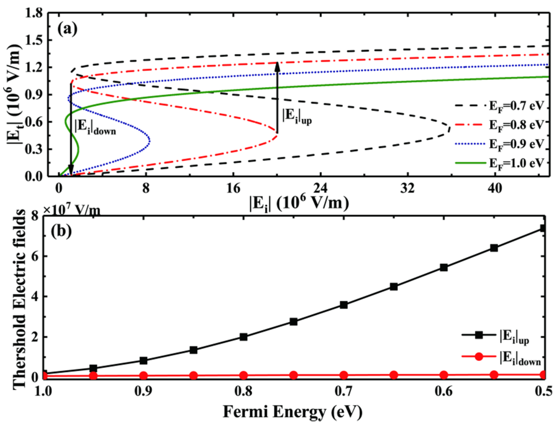
In this section, we first talk over the relevance between the transmitted electric field and the incident electric field under various Fermi energies in 3D DSM, while keeping the other values as those mentioned in Figure 1. Furthermore, it should be noted that since this work is purely theoretical, we did not consider the influence of edge effects on multilayer structures. The key factor in realizing OB in this study is the large nonlinear conductivity of Dirac semimetals. Specifically, when we fill 3D DSM into the FP cavity, we observe a significant change in the relevance curve between and , resulting in a hysteresis loop in the transmission curve. This is because the conditions required to achieve OB become easier to satisfy when the 3D DSM are filled into the FP cavity. Figure 2 clearly illustrates the effect of changes in Fermi energy on the threshold of optical bistability. From Figure 2, it can be seen that an increase in the Fermi energy can slightly lower the threshold of optical bistability. Although the threshold reduction is not significant, it cannot be denied that it is beneficial after all. However, the increase in the Fermi energy also leads to a sharp decrease in the threshold width, and even causes the disappearance of bistable phenomena, which is something we do not want to see. From Figure 2a, we can see that when is small, the transmitted electric field gradually raises with the incident electric field until a specific value, at which point the transmitted electric field undergoes a jump. However, when is large, gradually decreases with up to a specific value, at which point undergoes a jump. In the case of the double stable curve at in the figure, when gradually increases from a small value to , the transmitted electric field undergoes an upward mutation, and the value of at this point is called the upper threshold field of the switch. However, when the incident electric field gradually decreases from a large value to , the transmitted electric field undergoes a downward mutation, and the value of at this point is called the lower threshold field of the switch. In addition, the hysteresis width is denoted as . Moreover, from Figure 2a, we can also observe that as the Fermi energy of the 3D DSM increases, both the upper and lower threshold fields of the OB ( and ) raise, and they move to higher light intensity ranges to the right. We describe this phenomenon in detail in Figure 2b. As shown in the figure, as of the 3D DSM increases, the hysteresis loop between and gradually increases, and its hysteresis width also significantly widens because the speed of the upper threshold field of the OB moving to the right is much faster than that of the lower threshold field of the OB. Additionally, we can find that, although reducing of the 3D DSM is advantageous for lowering the OB threshold, when the Fermi energy decreases to a certain extent, the hysteresis width disappears and the OB curve vanishes as well. In summary, the discovery of the above laws is beneficial for us to regulate the OB threshold and hysteresis width by adjusting of the 3D DSM, providing a pathway for people to regulate the OB phenomenon through external electric field control.
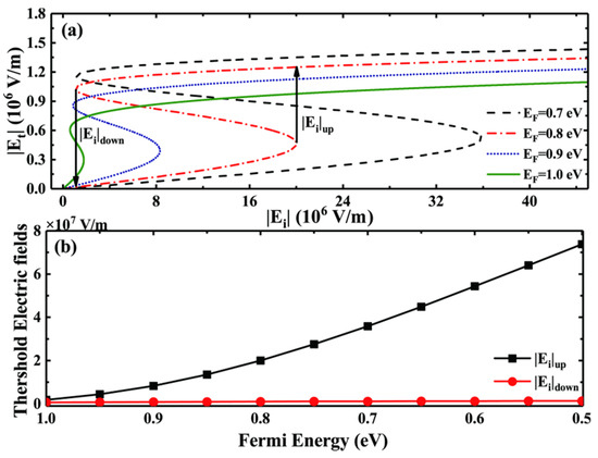
Figure 2.
(a) Dependence of on for different Fermi energies; (b) the influence of the Fermi energy of the 3D DSM on threshold.
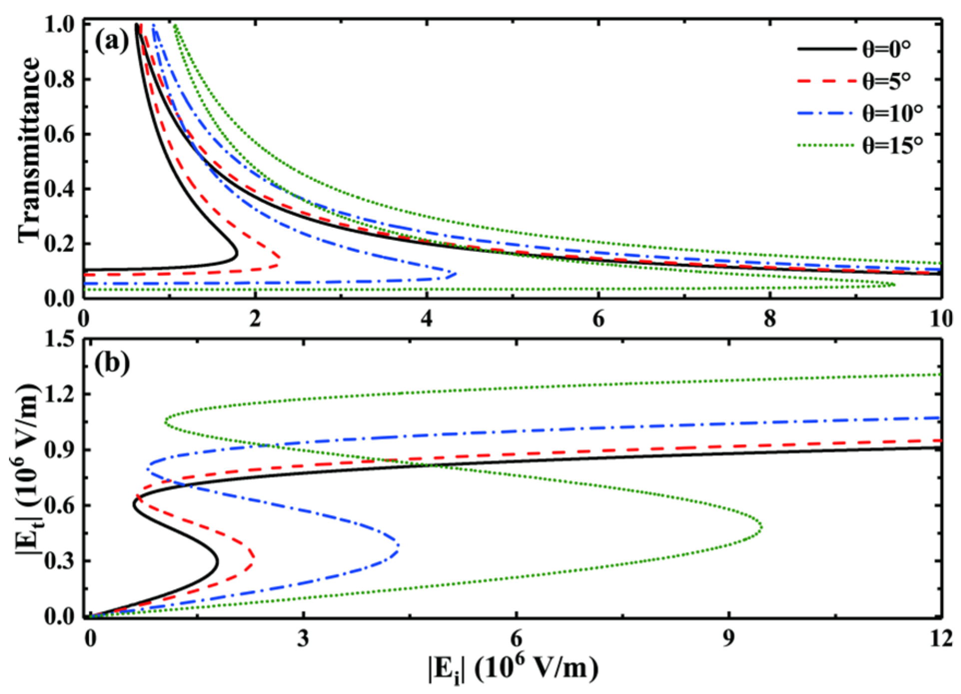
Next, we will discuss the impact of incident angle variations on the OB curve. We set the Fermi energy as , and other values were kept consistent with Figure 1. As illustrated in Figure 3, the threshold size and hysteresis width of the OB change with the incident angle, indicating that the OB phenomenon is highly sensitive to the incident angle, which follows a similar pattern to the discussion on the 3D DSM Fermi energy in the previous section. As shown in Figure 3a, increasing the incident angle of the structure causes the transmittance curve to shift towards higher light intensities, and the hysteresis width gradually increases with increasing incident angle. Meanwhile, the dependence of on also exhibits a similar variation tendency; the above rule is reflected in Figure 3b. We take and as examples to analyze the changing pattern in detail: when , , , and the hysteresis width ; when , , , and the hysteresis width is . These calculated results confirm the above pattern well. In addition, as shown in the OB line at in Figure 3b, although the hysteresis width gradually narrows with decreasing incident angle, even when the incident angle decreases to , there is still a hysteresis width in the relevance curve between and . Therefore, it can be proven that the method of using the 3D DSM-based photonic crystal FP cavity to achieve low-threshold and tunable OB can also be implemented under vertical incidence conditions without requiring specific incident angles. Compared to certain traditional methods of achieving low-threshold OB, this method has more advantages and is easier to implement.
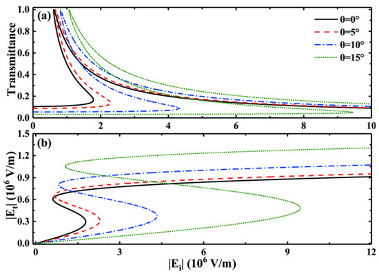
Figure 3.
Under various incidence angles, the relationship between (a) transmittance, (b) and .
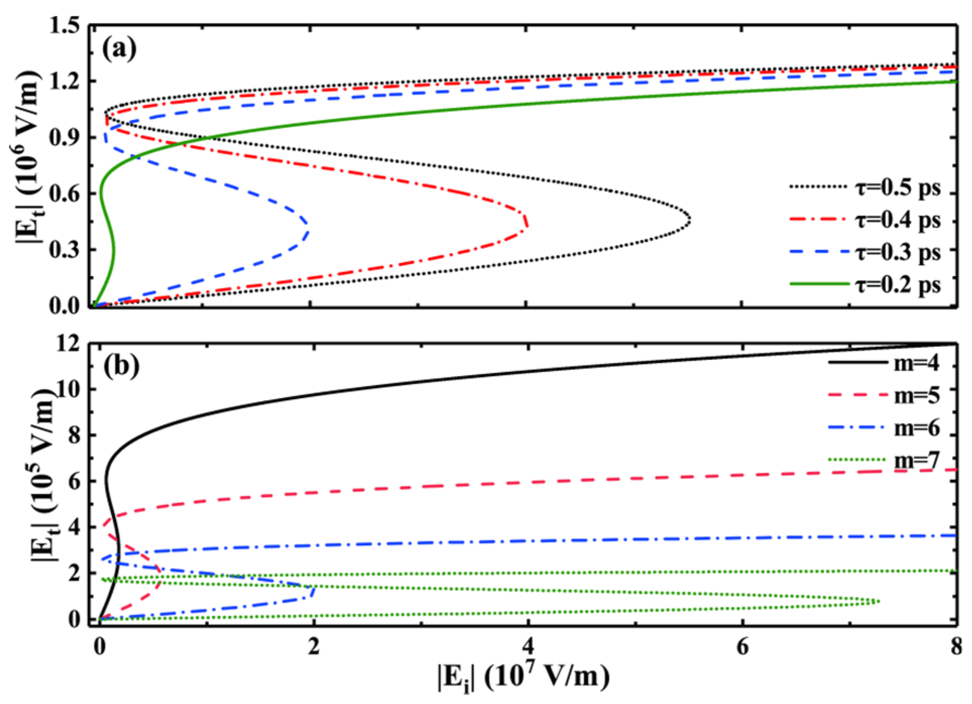
Furthermore, we investigate the influence of relaxation time and photonic crystal period variations on the OB phenomenon while keeping other relevant values unchanged. On the one hand, as illustrated in Figure 4a, we observe that the change in the relevance between and exhibits the same trends as those seen in the OB threshold and hysteresis width for different relaxation times. In the wake of decreases in , the OB threshold also decreases. However, when and both gradually increase but increases faster than , the hysteresis width rapidly narrows. For instance, when, , , and the hysteresis width is , and when , , and , it is . Simulation results reveal that the OB curve vanishes when the relaxation time expends to . Therefore, while reducing the relaxation time can effectively lower the OB threshold, it cannot be reduced to an excessively low level, as this will cause the OB phenomenon to disappear. On the other hand, as showed in Figure 4b, we find that the impact of photonic crystal period variations on the OB phenomenon is highly similar to that of relaxation time. The OB threshold decreases as the photonic crystal period decreases, and the hysteresis width between and narrows. Thus, careful consideration is required in choosing both the relaxation time and photonic crystal period to ensure optimal OB phenomenon production and the fabrication of more reasonable and practical OB devices.
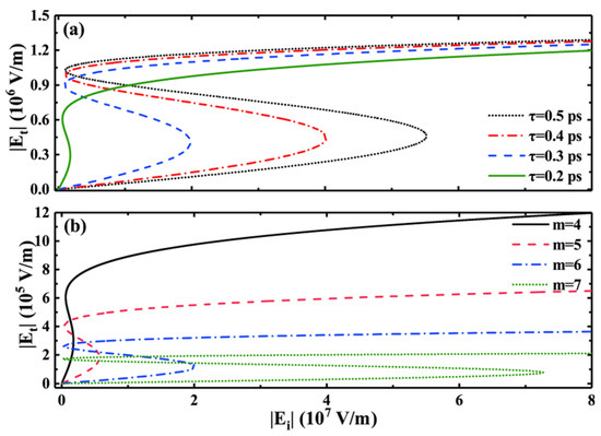
Figure 4.
The relationship between and at (a) different relaxation times and (b) different photonic crystal periods.
Regarding the relevance between and , we observed that the OB phenomenon is not only sensitive to the relaxation time, photonic crystal period, and 3D DSM Fermi energy but also to the cavity length of the FP cavity and the position of the 3D DSM layer in the cavity. Firstly, with the cavity length fixed at , we studied the effect of the placement of the 3D DSM layer in the cavity on the OB phenomenon. The position of the center point of the 3D DSM layer can be represented as . As shown in Figure 5a, as the position of the 3D DSM layer in the FP cavity changes, the resulting OB phenomenon also changes, with a corresponding change in the threshold size and hysteresis width, thus achieving flexible control of the OB phenomenon by adjusting the position of the 3D DSM layer. Additionally, the cavity length of the FP cavity should satisfy , where the frequency is inversely proportional to the cavity length . Therefore, by adjusting the cavity length , the OB phenomenon can be controlled. Figure 5b shows the changes in the hysteresis curve after changing the cavity length. It can be observed that as the cavity length increases, the threshold size and hysteresis width of the OB phenomenon both increase significantly. Thus, we believe that the cavity length of the FP cavity can be an important means of controlling the OB phenomenon.
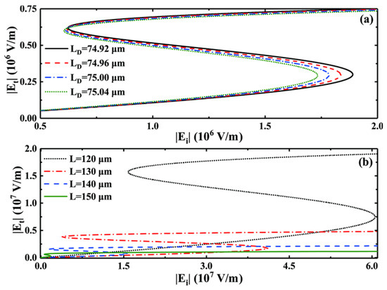
Figure 5.
(a) Variation of the cavity length and (b) relevance between and for different positions of the 3D DSM layer inside the cavity.
4. Conclusions
In conclusion, we have studied the OB phenomenon in a photonic crystal FP cavity based on 3D DSM. By utilizing the unique band structure of the photonic crystal, the resonant effect of the FP cavity, and the extraordinary nonlinear properties of 3D DSM, we have achieved low-threshold OB at terahertz frequencies, which can be flexibly controlled in terms of threshold size and hysteresis width. Our theoretical studies have shown that embedding 3D DSM in a FP cavity can significantly enhance the hysteresis behavior. By adjusting parameters such as the Fermi energy of the 3D DSM, the incident angle of the beam, the relaxation time, the cavity length of the FP cavity, and the position of the 3D DSM layer in the FP cavity, the OB phenomenon can be further controlled. Through numerical simulations, we have found suitable 3D DSM and structural parameters and obtained an OB curve with a threshold of . Our research provides new ideas for achieving tunable low-threshold OB at terahertz frequencies. We are firmly convinced that the construction described within this article for realizing OB is relatively simple, has advantages in the manufacture of practical OB devices, and has an extensive range of applications in the field of nonlinear optical devices.
Author Contributions
Methodology, Y.Y.; Formal analysis, W.C.; Resources, Y.Y.; Data curation, J.P.; Writing—original draft, H.Z.; Writing—review & editing, R.W. All authors have read and agreed to the published version of the manuscript.
Funding
This work was supported by the Wenzhou major science and technology innovation project: Research and Industrialization of Key Technologies for Intelligent Dynamic Ultrahigh Pressure Microfluidizer (Grant No. ZG2023012), the Wenzhou major science and technology innovation project (Grant No. ZG2022011), and the science and technology project of Zhejiang Province (Grant No. 2024C25030).
Institutional Review Board Statement
Not applicable.
Informed Consent Statement
Not applicable.
Data Availability Statement
Data are contained within the article.
Conflicts of Interest
The authors declare no conflict of interest.
References
- Boyd, R.W. Nonlinear Optics; Academic Press, Inc.: San Diego, CA, USA, 1992. [Google Scholar]
- Gibbs, H.M. Optical Bistability Controlling: Light with Light; Academic Press: Cambridge, MA, USA, 1985. [Google Scholar]
- Li, J.B.; Liang, S.; Xiao, S.; He, M.D.; Liu, L.H.; Luo, J.H.; Chen, L.Q. A sensitive biosensor based on optical bistability in a semiconductor quantum dot-DNA nanohybrid. J. Phys. D Appl. Phys. 2019, 52, 035401. [Google Scholar] [CrossRef]
- Notomi, M.; Shinya, A.; Mitsugi, S.; Kira, G.; Tanabe, T. Optical bistable switching action of Si high-Q photonic-crystal nanocavities. Opt. Express 2005, 13, 2678–2687. [Google Scholar] [CrossRef]
- Yanik, M.F. All-optical transistor action with bistable switching in a photonic crystal cross-waveguide geometry. Opt. Lett. 2003, 28, 2506–2508. [Google Scholar] [CrossRef] [PubMed]
- Tanabe, T.; Notomi, M.; Mitsugi, S.; Shinya, A.; Kuramochi, E. Fast bistable all-optical switch and memory on a silicon photonic crystal on-chip. Opt. Lett. 2005, 30, 2575–2577. [Google Scholar] [CrossRef] [PubMed]
- Bravo-Abad, J.; Rodriguez, A.; Bermel, P.; Johnson, S.G.; Joannopoulos, J.D.; Soljačić, M. Enhanced nonlinear optics in photonic-crystal micro-cavities. Opt. Express 2007, 15, 16161–16176. [Google Scholar] [CrossRef] [PubMed]
- Azadpour, F.; Bahari, A. All-optical bistability based on cavity resonances in nonlinear photonic crystal slab-reflector-based Fabry-Perot cavity. Opt. Commun. 2018, 437, 297–302. [Google Scholar] [CrossRef]
- Zang, Z.G. Numerical analysis of optical bistability based on Fiber Bragg Grating cavity containing a high nonlinearity doped-fiber. Opt. Commun. 2011, 285, 521–526. [Google Scholar] [CrossRef]
- Wang, G.; Lu, H.; Liu, X.; Gong, Y.; Wang, L. Optical bistability in metal-insulator-metal plasmonic waveguide with nanodisk resonator containing Kerr nonlinear medium. Appl. Opt. 2011, 50, 5287–5290. [Google Scholar] [CrossRef] [PubMed]
- Wysin, G.; Simon, H.; Deck, R. Optical bistability with surface plasmons. Opt. Lett. 1981, 6, 30–32. [Google Scholar] [CrossRef]
- Gosciniak, J.; Hu, Z.; Thomaschewski, M.; Sorger, V.J.; Khurgin, J.B. Bistable All-Optical Devices Based on Nonlinear Epsilon-Near-Zero (ENZ) Materials. Laser Photonics Rev. 2023, 17, 2200723. [Google Scholar] [CrossRef]
- Liu, M.; Yin, X.; Ulin-Avila, E.; Geng, B.; Zentgraf, T.; Ju, L.; Wang, F.; Zhang, X. A graphene-based broadband optical modulator. Nature 2011, 474, 64–67. [Google Scholar] [CrossRef] [PubMed]
- Bonaccorso, F.; Sun, Z.; Hasan, T.; Ferrari, A.C. Graphene photonics and optoelectronics. Nat. Photonics 2011, 4, 611–622. [Google Scholar] [CrossRef]
- Jiang, L.Y.; Tang, J.; Xu, J.; Zheng, Z.W.; Dong, J.; Guo, J.; Qian, S.Y.; Dai, X.Y.; Xiang, Y.J. Graphene Tamm plasmon-induced low-threshold optical bistability at terahertz frequencies. Opt. Mater. Express 2019, 9, 139–150. [Google Scholar] [CrossRef]
- Deng, H.Q.; Ji, C.P.; Zhang, X.Y.; Chen, P.; Wu, L.C.; Jiang, J.; Tian, H.S.; Jiang, L.Y. Low threshold optical bistability in graphene/waveguide hybrid structure at terahertz frequencies. Opt. Commun. 2021, 499, 127282. [Google Scholar] [CrossRef]
- Jiang, L.Y.; Guo, J.; Wu, L.M.; Dai, X.Y.; Xiang, Y.J. Manipulating the optical bistability at terahertz frequency in the Fabry-Perot cavity with graphene. Opt. Express 2015, 23, 31181–31191. [Google Scholar] [CrossRef] [PubMed]
- Liang, T.; Gibson, Q.; Ali, M.N.; Liu, M.; Cava, R.J.; Ong, N.P. Ultrahigh mobility and giant magnetoresistance in the Dirac semimetal Cd3As2. Nat. Mater. 2015, 14, 280–284. [Google Scholar] [CrossRef] [PubMed]
- Neupane, M.; Xu, S.Y.; Sankar, R.; Alidoust, N.; Bian, G.; Liu, C.; Belopolski, I.; Chang, T.R.; Jeng, H.T.; Lin, H.; et al. Observation of a three-dimensional topological Dirac semimetal phase in high-mobility Cd3As2. Nat. Commun. 2014, 5, 3786. [Google Scholar] [CrossRef]
- Kotov, O.V.; Loxovik, Y.E. Dielectric response and novel electromagnetic modes in three dimensional Dirac semimetal films. Phys. Rev. B 2016, 93, 235417. [Google Scholar] [CrossRef]
- Kim, D.S.; Kim, D.H.; Hwang, S.; Jang, J.H. Broadband terahertz absorber realized by selfassembled multilayer glass spheres. Opt. Express 2012, 20, 13566–13572. [Google Scholar] [CrossRef]
- Ooi, K.J.A.; Ang, Y.S.; Zhai, Q.; Tan, D.T.H.; Ang, L.K.; Ong, C.K. Nonlinear plasmonics of three-dimensional Dirac semimetal. APL Photonics 2019, 4, 034402. [Google Scholar] [CrossRef]
- Hou, P.; Chen, Y.; Chen, X.; Shi, J.; Wang, Q. Giant bistable shifts for one-dimensional nonlinear photonic crystals. Phys. Rev. A 2007, 75, 045802. [Google Scholar] [CrossRef]
- Long, X.; Bao, Y.W.; Yuan, H.X.; Zhang, H.Y.; Dai, X.Y.; Li, Z.F.; Jiang, L.Y.; Xiang, Y.J. Low threshold optical bistability based on topological edge state in photonic crystal heterostructure with Dirac semimetal. Opt. Express 2022, 30, 20847–20858. [Google Scholar] [CrossRef] [PubMed]

Disclaimer/Publisher’s Note: The statements, opinions and data contained in all publications are solely those of the individual author(s) and contributor(s) and not of MDPI and/or the editor(s). MDPI and/or the editor(s) disclaim responsibility for any injury to people or property resulting from any ideas, methods, instructions or products referred to in the content. |
© 2024 by the authors. Licensee MDPI, Basel, Switzerland. This article is an open access article distributed under the terms and conditions of the Creative Commons Attribution (CC BY) license (https://creativecommons.org/licenses/by/4.0/).