Article

Nonlinear Optical Bistability Based on Surface Plasmons with Nonlinear Dirac Semimetal Substrate

1
College of Science, Jiujiang University, Jiujiang 332005, China
2
School of Mechanical and Intelligent Manufacturing, Jiujiang University, Jiujiang 332005, China
3
School of Physics and Electronics, Hunan Normal University, Changsha 410081, China
*
Author to whom correspondence should be addressed.
Coatings 2024, 14(4), 394; https://doi.org/10.3390/coatings14040394
Submission received: 29 October 2023 / Revised: 17 March 2024 / Accepted: 24 March 2024 / Published: 27 March 2024
(This article belongs to the Special Issue Optical Properties of Crystals and Thin Films, Volume II)

Abstract

:
In this paper, we theoretically investigated the low-threshold and controllable optical bistability (OB) of a graphene-based Otto configuration with a nonlinear three-dimensional Dirac semimetal (3D DSM) as the substrate. The combined effect of the excitation of surface plasmon polaritons (SPPs) in graphene and the very high third-order nonlinear conductivity of the 3D DSM enabled this scheme to achieve a relatively low optical bistability threshold. At the same time, this simple multilayer structure showed the tunability of OB due to the fact that the reflectance could be modulated by regulating the Fermi energy of the 3D DSM. Furthermore, we also found that the OB hysteresis curve was closely related to the relaxation time of the 3D DSM and the thickness of the air layer. We believe that this multilayer configuration could provide a reference idea for devising a bistable device.

1. Introduction

Optical bistability (OB) is a fascinating nonlinear optical phenomenon that exhibits a clear hysteresis loop relationship between the output and input light intensity, characterized by two corresponding output intensities for a given input intensity [1]. The OB phenomenon has excellent nonlinear optical properties and has been widely used in various micro–nano optoelectronic devices in recent years, such as biosensors [2], all-optical switches [3], optical memory [4], optical logic devices [5], optical transistors [6], etc. With the increasing demand for micro–nano optoelectronic devices and the maturity of micro–nano fabrication technology, more and more researchers are focusing on the design of micro–nano optically bistable devices. Recently, a number of micro–nano structures have been proposed for OB implementation, such as Fabry–Perot cavities [7], hyperbolic metamaterials [8], photonic crystals [9], and optical ring cavities [10]. It is well known that threshold and response time are two important indicators for evaluating optically bistable devices. As there is currently no urgent need for fast response time in communication systems, researchers are focusing on how to achieve low-threshold OB. Large incident light intensity is one of the necessary conditions to obtain an obvious OB phenomenon, but this often leads to device damage, which significantly hinders the development of optically bistable devices. To address this challenge, structures with locally enhanced fields, such as the defect mode in photonic crystals [11], the optical Tamm state [12], and the topological edge state [13], have been proposed. Surface plasmon polaritons (SPPs) are highly localized electromagnetic modes that arise from strong interactions between metal surface free electrons and incident photons [14]. They can be excited through prism coupling, near-field excitation, grating coupling, strong focusing beams [15], etc. Common prism coupling methods include the Krestchmann structure [16] and the Otto structure [17]. Specifically, the local field enhancement exhibited by graphene SPPs allows for the observation of a significant OB phenomenon at lower incident light intensity, providing favorable conditions for achieving low-threshold OB. In addition, finding materials with higher nonlinear refractive indices is also one of the directions for studying low-threshold OB. In recent years, graphene has played an important role in the field of nonlinear optics, owing to its considerable nonlinear conductivity and excellent optoelectronic properties. Nonlinear optical devices based on graphene, such as optical switches [18], biomedical sensing elements [19], memory [20], etc., have been extensively studied. Although graphene’s remarkable nonlinearity and controllability have led to extensive research in the field of nonlinear optics, its limitations in preparation and operational bandwidth cannot be ignored. Recently, Dirac materials, represented by three-dimensional Dirac semimetals (3D DSMs), have become a research hotspot [21,22]. They are known as “3D graphene” and have optical properties that are similar to or even better than those of graphene [23]. Like graphene, these materials also have excellent optoelectronic properties but present higher carrier mobility and stronger light–matter coupling and are easier to prepare [24]. In addition, their Fermi energy can be changed through modulation of external voltage or chemical doping, providing the possibility of designing controllable micro–nano optoelectronic devices [25]. Especially, their higher nonlinear refractive indices provide the necessary nonlinear conditions for achieving low-threshold OB [13,26]. Therefore, it is expected that these materials will replace graphene as the new generation of materials for preparing various micro–nano nonlinear optically bistable devices.
In summary, this article proposes an Otto structure based on 3D DSMs, which excites graphene SPPs through prism coupling. The results indicate that the emergence of strong localized fields is due to the excitation of SPPs at the interface between air and graphene. Moreover, the considerable nonlinear refractive index of the substrate 3D DSM provides a nonlinear refractive index for achieving OB. In addition, the relevant parameters of graphene and the 3D DSM, such as Fermi energy and relaxation time, have a significant regulatory effect on the OB phenomenon. We further found that changing structural parameters can apparently regulate the OB phenomenon. We believe that this structure provides a new approach for achieving controllable OB and can be applied in the field of nonlinear photons.

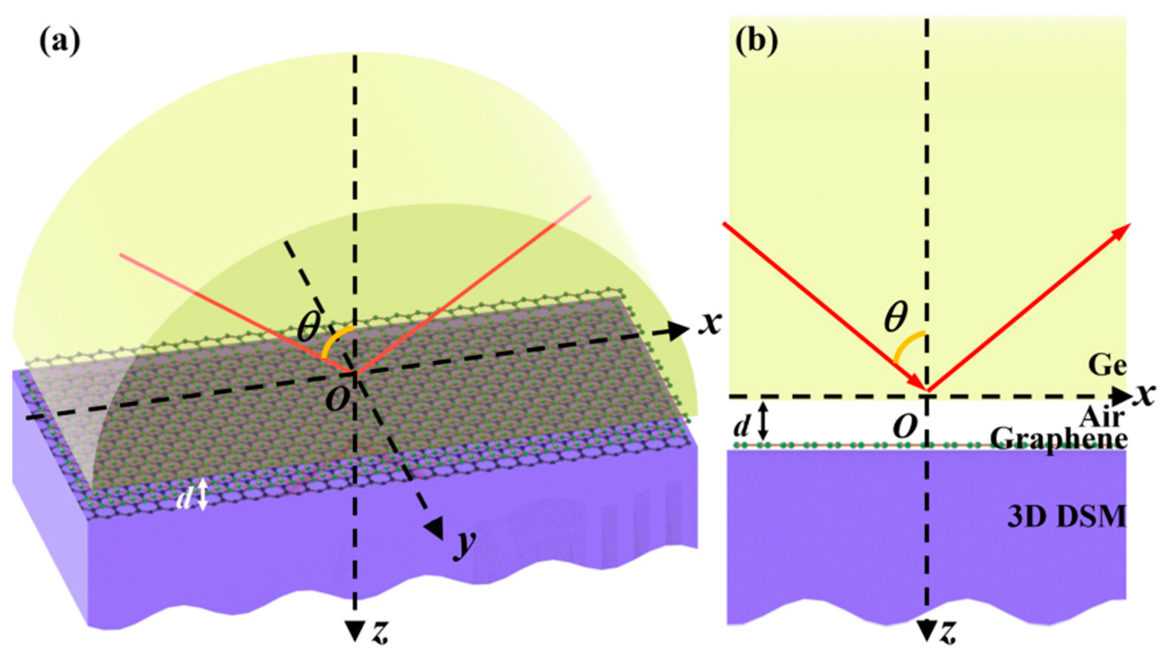
2. Theoretical Model and Method

We consider an Otto structure based on a 3D DSM, as shown in Figure 1. A germanium prism is separated from the 3D DSM by an air layer, and graphene covers the semi-infinite 3D DSM surface. The proposal of this structure is also based on the convenient acquisition of low-threshold optical bistability. First, we construct the SPP structure with localized field enhancement. The Otto configuration is a typical structure for exciting SPPs. Secondly, we need to select a nonlinear material with a large nonlinear coefficient to provide the necessary nonlinear characteristics for generating optical bistable phenomena, so we choose a nonlinear 3D DSM as the substrate. Based on the above comprehensive considerations, we propose the structure shown in Figure 1. Since SPPs are only excited in TM polarization, this paper only discusses the latter. We assume that the electromagnetic wave is incident on the germanium prism at an angle θ and wavelength λ = 100   μ m . The refractive indices of the germanium prism and the air layer are denoted by n p = 3.84  and, n 1 = 1 respectively. It should be noted that the core purpose of this work is to achieve optical bistability with as low a threshold as possible. Therefore, the initial values of structural and material parameters are selected based on program optimization. Based on this, we first set the thickness of the air layer to d = 3.5   μ m . Additionally, the optical properties of graphene are generally characterized by its surface conductivity, and its linear intraband and interband conductivity can be obtained with the Kubo formula [27]:
{ σ g - intra ( 1 ) = i e 2 k B T π 2 ( ω + i / τ ) ( E F k B T + 2 ln ( e E F k B T + 1 ) ) σ g - inter ( 1 ) = i e 2 4 π ln | 2 E F ( ω + i τ 1 ) 2 E F + ( ω + i τ 1 ) | ,
where E F and τ are the Fermi energy and relaxation time of graphene, respectively. e , k B , , and ω represent the charge of an electron, the Boltzmann constant, the reduced Planck constant, and the angular frequency of the incident light, respectively. T = 300   K is the temperature. In the terahertz frequency range, the interband conductivity of graphene can be neglected. Therefore, for convenience, the linear conductivity of graphene in this paper is approximated as σ g ( 1 ) σ g - intra ( 1 ) . In addition, the optoelectronic properties of 3D DSMs can also be expressed in terms of conductivity. We know that unlike graphene, 3D DSM is a general term for a class of materials. In order to combine practice and facilitate the calculations, in the subsequent computations of this article, we choose cadmium arsenide (Cd3As2) to represent the specific 3D DSM material. Its linear conductivity can be approximated as [26]
σ d ( 1 ) = σ 0 4 3 π 2 τ D 1 i ω τ D ( k B T ) 2 2 v F [ 2 L i 2 ( e E F D k B T ) + ( E F D k B T ) 2 + π 2 3 ] ,
where σ 0 e 2 / 4 ; τ D and E F D are the relaxation time and Fermi energy of the 3D DSM, respectively; v F is the Fermi velocity of electrons; and L i s ( z ) is the multiple logarithmic function. The linear part of the refractive index of the 3D DSM can be expressed as n D = 1 + i σ d ( 1 ) / ε 0 ω , so its linear dielectric constant is represented by ε D = n D 2 , where ε 0 is the absolute dielectric constant. Furthermore, the nonlinear conductivity of Cd3As2 is given by [26]
σ d ( 3 ) = σ 0 8 e 2 v F 5 π 2 2 τ D 3 ( 1 + ω 2 τ D 2 ) ( 1 2 i ω τ D ) 1 ( 1 + exp ( E F D / ( k B T ) ) ) .
Then, the third-order nonlinear susceptibility of Cd3As2 is χ ( 3 ) = χ ( 3 ) + i χ ( 3 ) = i σ d ( 3 ) / ε 0 ω , the effective third-order nonlinear susceptibility is χ e ( 3 ) = 3 χ ( 3 ) , and the nonlinear refractive index can be expressed as n 2 = χ e ( 3 ) / 2 n D . In order to simplify the calculations, except for the additional parameter values set in this paper, the other initial parameters of the linear and nonlinear conductivity of Cd3As2 are consistent with those in [26]. Additionally, the transmission characteristics of the 3D DSM are described by wave equations. As a typical Kerr nonlinear medium, the wave equation for the magnetic field ( H 2 y ) of the 3D DSM can be expressed as [28,29]
2 H 2 y z 2 + k 0 2 ( ε D + α | H 2 y | 2 ε p sin 2 θ ) H 2 y = 0 ,
where ε p is the dielectric constant of the prism, α = α / ( ε D ε 0 2 c 2 ) , and α = ε D ε 0 c n 2 is the nonlinear coefficient ( ε 2 = ε D + α | E | 2 ) of the 3D DSM. For self-focusing Kerr nonlinear media, the solution to the wave equation can be written as
H 2 y ( z ) = 2 / α q sech [ k 0 q ( z d ) + κ ] exp i ( C + k x x ω t ) ,
where C is a constant, q 2 = ε p sin 2 θ ε D , κ = cosh 1 ( 2 / α q / | H 2 y ( z = d ) | ) , and H 2 y ( z = d ) is the magnetic field amplitude of the 3D DSM surface covered with graphene. The transmission and reflection coefficients of the structure can be calculated by using the Fresnel formula, according to which the reflection and transmission coefficients at the interface between the germanium prism and the air layer can be written as
{ r p 1 = k p z / ε p k 1 z / ε 1 k p z / ε p + k 1 z / ε 1 t p 1 = 2 k p z / ε p k p z / ε p + k 1 z / ε 1 ,
where k p z = k 0 ε p cos θ and k 1 z = k 0 ε 1 ε p sin 2 θ are the components of the wave vector in the z-direction in the germanium prism and air, respectively. The reflection and transmission coefficients at the interface between the air layer and the 3D DSM can be written as
{ r 12 = k 1 z / ε 1 ( 1 + σ g ( 1 ) k 2 z e / ( ω ε 0 ε 2 e ) ) k 2 z e / ε 2 e k 1 z / ε 1 ( 1 + σ g ( 1 ) k 2 z e / ( ω ε 0 ε 2 e ) ) + k 2 z e / ε 2 e t 12 = 2 k 1 z / ε 1 k 1 z / ε 1 ( 1 + σ g ( 1 ) k 2 z e / ( ω ε 0 ε 2 e ) ) + k 2 z e / ε 2 e ,
where k 2 z e = i k 0 q tanh ( κ ) is the effective wave vector component in the z-direction in the 3D DSM, ε 2 e = ε D + α | H 2 y ( z = d ) | 2 / 2 is the effective dielectric constant of the 3D DSM, and σ g ( 1 ) is the linear complex electric conductivity of graphene. It is worth noting that although Equation (7) still has the form of the Fresnel formula as a whole, it needs to be modified due to the effect of the graphene layer on boundary conduction. When σ g ( 1 ) = 0 , i.e., the interface between air and the 3D DSM is not covered with graphene, Equation (7) becomes the general Fresnel formula. The total reflection and transmission coefficients of the light at the interface between air and the 3D DSM covered by graphene can be expressed as
{ r = r p 1 + r 12 exp ( 2 i k 1 z d ) 1 + r p 1 r 12 exp ( 2 i k 1 z d ) t = t p 1 t 12 exp ( i k 1 z d ) 1 + r p 1 r 12 exp ( 2 i k 1 z d ) .
In addition, the relationship between a given magnetic field H 2 y ( z = d ) and the input light intensity can be written as
I i n = 1 2 c ε 0 ε p | H 2 y ( z = d ) | 2 | t | 2 .
Then, the corresponding reflection light intensity ( I r e ) and the reflection electric field ( E r e ), the transmission light intensity ( I o u t ), and the transmission electric field ( E o u t ) can be obtained based on the calculated reflection and transmission rates.

3. Results and Discussion

We will first discuss the influence of the Fermi energies of the two materials on the reflectivity of the entire multilayer structure. Figure 2a,b show the influence of the graphene ( E F ) and 3D DSM Fermi energies ( E F D ) on the reflection spectra, respectively. It should be noted that in Figure 2, we have set these parameters within a certain range of values based on the proposed structure, using corresponding calculation programs and continuous debugging over a long period of time. In the Introduction section, we mentioned that the core indicator of optical bistability is to achieve the lowest possible threshold. This requires us to further adjust or optimize the parameters to obtain the lowest possible threshold after obtaining obvious OB phenomena. Therefore, in the Discussion section, the numerical selection of the Fermi energies of the two materials is also aimed at obtaining the lowest possible threshold based on the scheme in Figure 1. From Figure 2a, it can be seen that when there is no graphene in the structure; there is only one dip in the reflection spectrum, which is caused by the electromagnetic wave under normal incidence. After inserting graphene, the reflection spectrum changes significantly, with a second resonance peak appearing. This peak comes from the excitation of graphene SPPs, and the excitation angle can be easily obtained through the corresponding dispersion curve [30]. Unlike the first dip, which remains stable, the second resonance peak is clearly influenced by the graphene ( E F ) and 3D DSM Fermi energies ( E F D ). As can be seen from Figure 2a, as E F increases, the second resonance angle gradually decreases, and so does the reflectance. At the same time, the reflection spectrum characteristics are also regulated by E F D . When E F D continues to increase, the second resonance angle also increases, and so does the reflectance. These regulatory characteristics provide rich means for realizing controllable OB phenomena.
Next, we will discuss in detail the regulatory effects of structural and material parameters on the OB phenomenon, focusing on the 3D DSM Fermi energy ( E F D ) first. Figure 3a,b show the functional relationships between the reflected electric field/reflectance and the incident electric field, as well as how the threshold and hysteresis loop width of OB vary with E F D . From Figure 3a, we can see that as E F D increases from 0.63 eV to 0.66 eV, both the upper and lower thresholds of OB decrease continuously, and so does the hysteresis loop width. Specifically, if E F D is 0.63 eV, the upper and lower thresholds of OB are | E i | u p 3.71 × 10 6   V / m and | E i | d o w n 4.99 × 10 6 V / m , with the threshold width of Δ Y = 1.28 × 10 6   V / m ; if E F D is 0.66 eV, the upper and lower thresholds of OB are | E i | u p 3.23 × 10 6   V / m and | E i | d o w n 3 . 47 × 10 6 V / m , with the threshold width of Δ Y = 0.24 × 10 6   V / m . Figure 3b shows the dependence of reflectance on the incident electric field for different 3D DSM Fermi energies ( E F D ) corresponding to Figure 3a, with their changing trends remaining consistent. The dynamic tunability of 3D DSMs provides a basis for achieving controllable OB. The behavior of OB can be controlled solely by adjusting the external voltage applied to the Dirac semimetal.
It is well known that the Fermi energy of Dirac materials can be effectively controlled by adjusting the external voltage or chemical doping applied to them. Therefore, changing the Fermi energy ( E F ) of graphene is an effective method to control the OB phenomenon. Figure 4a,b show the relationship between the reflected electric field/reflectance and the incident electric field, respectively, for different graphene Fermi energies ( E F ). We can see that the OB phenomenon is also influenced by E F . The threshold width and upper and lower thresholds of OB increase with the increase in E F , with the lower threshold changing more than the upper threshold. When E F increases from 0.77 eV to 0.80 eV, the upper threshold increases by 0.24 × 10 6   V / m , and the lower threshold increases by 0.98 × 10 6   V / m . We can see that changing E F can also sensitively control the OB phenomenon and allows the low-threshold OB required for optical bistable devices to be achieved.
In addition to the Fermi energy, the relaxation time can also be used to regulate the hysteresis behavior of OB. Figure 5 shows the functional relationship between the reflected electric field/reflectance and the incident electric field at different relaxation times. Figure 5a,b show the effect of the relaxation time ( τ D ) of the 3D DSM on OB and Figure 5c,d that of the relaxation time ( τ ) of graphene on OB. From Figure 5, we can clearly see that compared with the relaxation time of graphene, τ D has a more significant effect on the control of OB, which is also inconsistent in trend. When τ D increases, the thresholds and threshold width of OB also increase; when τ continuously increases, the hysteresis loop width of OB gradually increases, but its upper and lower thresholds continue to decrease. It is worth noting that although the role of relaxation time in controlling the OB threshold is very obvious, it still has limitations in flexibility. After all, once the 3D DSM and graphene materials are prepared, their relaxation time no longer has controllable characteristics. Nevertheless, we have still discussed the effect of relaxation time on OB, which provides a reference for the design of bistable devices.
The tunable optical properties of 3D DSMs and graphene make it possible to employ various methods and approaches for realizing low-threshold and tunable OB. We have already discussed in detail how to adjust the OB phenomenon by changing the relevant parameters of the 3D DSM. In addition, proper adjustments to OB can also be made by changing the corresponding structural parameters. Figure 6 shows the effects of different air layer thicknesses (d) on the threshold and hysteresis loop width of OB. As can be seen from the figure, as d increases, the OB thresholds and threshold widths also increase, with this effect being significant. In principle, the OB devices we design should be as small as possible for device integration, and a smaller air layer thickness value can result in a lower OB threshold. Therefore, in theory, we should make the air layer thin enough when designing OB devices with an Otto structure, which is beneficial for achieving low-threshold OB. However, small-sized devices have higher process requirements, and the errors caused by constructing devices of this type are usually large, which is very unfavorable for the design and manufacturing of low-threshold OB devices. Therefore, when designing optical devices, it is generally necessary to consider the balance between device performance and device process. At this time, theoretical analysis and calculation of the device provide important reference for this balance.

4. Conclusions

In summary, a 3D DSM-based Otto structure which can achieve low-threshold and tunable OB in the terahertz frequency range is proposed in this paper. The results show that graphene SPPs excited by the Otto structure can effectively enhance the local electric field, providing the necessary conditions for the implementation of low-threshold OB. In addition, the introduction of a 3D DSM provides crucial nonlinear conditions for achieving nonlinear OB. Moreover, the dynamically tunable optoelectronic properties of 3D DSMs provide a new approach for the tunability of OB. It is demonstrated that the Fermi energy and relaxation time of 3D DSMs play a crucial role in nonlinear OB, and reasonable adjustment of the relevant parameters can significantly lower the threshold of the hysteresis loop. Similarly, the Fermi energy and relaxation time of graphene also affect the OB phenomenon, providing another means of tuning for achieving controllable bistable phenomena. Finally, we discuss the effect of air layer thickness on OB, and the results show that the structural changes have a significant impact on the nonlinear OB phenomenon. Therefore, when designing bistable devices, the influence of the structural parameters on device performance should be fully considered. In conclusion, our proposed scheme and conclusions provide a theoretical basis for designing and fabricating bistable devices, and this scheme has potential applications in the field of all-optical devices.

Author Contributions

Conceptualization, Q.W.; Software, Y.G.; Writing—original draft, X.W.; Writing—review & editing, X.L. All authors have read and agreed to the published version of the manuscript.

Funding

This work was supported by Science and Technology Project of Jiangxi Provincial Education Department (grant No. GJJ190911).

Informed Consent Statement

Not applicable.

Data Availability Statement

Data are contained within the article.

Conflicts of Interest

The authors declare no conflict of interest.

References

  1. Gibbs, H.M. Optical Bistability: Controlling Light with Light; Academic Press: Cambridge, MA, USA, 1985. [Google Scholar]
  2. Li, J.B.; Liang, S.; Xiao, S.; He, M.D.; Liu, L.H.; Luo, J.H.; Chen, L.Q. A sensitive biosensor based on optical bistability in a semiconductor quantum dot-DNA nanohybrid. J. Phys. D Appl. Phys. 2018, 52, 035401. [Google Scholar] [CrossRef]
  3. Liu, J.C.; Wang, F.L.; Han, J.Y.; Hao, Y.Z.; Yang, Y.D.; Xia, J.L.; Huang, Y.Z. All-optical switching and multiple logic gates based on hybrid square–rectangular laser. J. Light. Technol. 2020, 38, 1382–1390. [Google Scholar] [CrossRef]
  4. Nagasaki, Y.; Gholipour, B.; Ou, J.Y.; Plum, E.; MacDonald, K.F.; Takahara, J.; Zheludev, N.I. Optical bistability in shape-memory nanowire metamaterial array. Appl. Phys. Lett. 2018, 113, 021105. [Google Scholar] [CrossRef]
  5. Zhang, W.L.; Jiang, Y.; Zhu, Y.Y.; Wang, F.; Rao, Y.J. All-optical bistable logic control based on coupled Tamm plasmons. Opt. Lett. 2013, 38, 4092–4095. [Google Scholar] [CrossRef] [PubMed]
  6. Hu, W.; Jiang, J.; Xie, D.; Wang, S.; Bi, K.; Duan, H.; Yang, J.; He, J. Transient security transistors self-supported on biodegradable natural-polymer membranes for brain-inspired neuromorphic applications. Nanoscale 2018, 10, 14893–14901. [Google Scholar] [CrossRef] [PubMed]
  7. Jiang, L.Y.; Guo, J.; Wu, L.M.; Dai, X.Y.; Xiang, Y.J. Manipulating the optical bistability at terahertz frequency in the Fabry-Perot cavity with graphene. Opt. Express 2015, 23, 31181–31191. [Google Scholar] [CrossRef]
  8. Kim, M.; Kim, S.; Kim, S. Optical bistability based on hyperbolic metamaterials. Opt. Express 2018, 26, 11620–11632. [Google Scholar] [CrossRef] [PubMed]
  9. Ardakani, A.G.; Firoozi, F.B. Highly tunable bistability using an external magnetic field in photonic crystals containing graphene and magnetooptical layers. J. Appl. Phys. 2017, 121, 023105. [Google Scholar] [CrossRef]
  10. Chen, Y.Q.; Dong, L.J.; Fang, Y.; Wu, X.Z.; Wu, Q.Y.; Jiang, J.; Shi, Y.L. Bistable switching in electromagnetically induced-transparency-like meta-molecule. Appl. Phys. 2019, A125, 22. [Google Scholar] [CrossRef]
  11. Wang, L.G.; Zhu, S.Y. Giant lateral shift of a light beam at the defect mode in one-dimensional photonic crystals. Opt. Lett. 2006, 31, 101–103. [Google Scholar] [CrossRef]
  12. Tang, J.; Ye, Y.Y.; Xu, J.; Zheng, Z.W.; Jin, X.L.; Jiang, L.Y.; Jiang, J.; Xiang, Y. High-sensitivity terahertz refractive index sensor in a multilayered structure with graphene. Nanomaterials 2020, 10, 500. [Google Scholar] [CrossRef] [PubMed]
  13. Long, X.; Bao, Y.W.; Yuan, H.X.; Zhang, H.Y.; Dai, X.Y.; Li, Z.F.; Jiang, L.Y.; Xiang, Y.J. Low threshold optical bistability based on topological edge state in photonic crystal heterostructure with Dirac semimetal. Opt. Express 2022, 30, 20847–20858. [Google Scholar] [CrossRef] [PubMed]
  14. Maier, S.A. Plasmonics: Fundamentals and Applications; Springer: Berlin/Heidelberg, Germany, 2007; Volume 1, p. 245. [Google Scholar]
  15. Zayats, A.V.; Smolyaninov, I.I.; Maradudin, A.A. Nano-optics of surface plasmon polaritons. Phys. Rep. 2005, 408, 131–314. [Google Scholar] [CrossRef]
  16. Kretschmann, E. The determination of the optical constants of metals by excitation of surface plasmons. Z. Für Phys. A Hadron. Nucl. 1971, 241, 313–324. [Google Scholar] [CrossRef]
  17. Otto, A. Excitation of nonradiative surface plasma waves in silver by the method of frustrated total reflection. Z. Für Phys. A Hadron. Nucl. 1968, 216, 398–410. [Google Scholar] [CrossRef]
  18. Farmani, A.; Zarifkar, A.; Sheikhi, M.H.; Miri, M. Design of a tunable graphene plasmonic-on-white graphene switch at infrared range. Superlattice Microst. 2017, 112, 404–414. [Google Scholar] [CrossRef]
  19. Kumar, R.; Singh, R.; Hui, D.; Feo, L.; Fraternali, F. Graphene as biomedical sensing element: State of art review and potential engineering applications. Compos. Part B Eng. 2018, 134, 193–206. [Google Scholar] [CrossRef]
  20. Yang, Y.; Lee, J.; Lee, S.; Liu, C.H.; Zhong, Z.; Wei, L. Oxide resistive memory with functionalized graphene as built-in selector element. Adv. Mater. 2014, 26, 3693–3699. [Google Scholar] [CrossRef] [PubMed]
  21. Borisenko, S.; Gibson, Q.; Evtushinsky, D.; Zabolotnyy, V.; Buchner, B.; Cava, R.J. Experimental realization of a three-dimensional Dirac semimetal. Phys. Rev. Lett. 2014, 113, 027603. [Google Scholar] [CrossRef] [PubMed]
  22. Neupane, M.; Xu, S.-Y.; Sankar, R.; Alidoust, N.; Bian, G.; Liu, C.; Belopolski, I.; Chang, T.-R.; Jeng, H.-T.; Lin, H.; et al. Observation of a three-dimensional topological Dirac semimetal phase in high-mobility Cd3As2. Nat. Commun. 2014, 5, 3786. [Google Scholar] [CrossRef] [PubMed]
  23. Liu, Z.K.; Zhou, B.; Zhang, Y.; Wang, Z.J.; Weng, H.M.; Prabhakaran, D.; Mo, S.K.; Zhang, Y.; Shen, Z.X.; Fang, Z.; et al. Discovery of a three-dimensional topological Dirac semimetal, Na3Bi. Science 2014, 343, 864–867. [Google Scholar] [CrossRef] [PubMed]
  24. Liang, T.; Gibson, Q.; Ali, M.N.; Liu, M.; Cava, R.J.; Ong, N.P. Ultrahigh mobility and giant magnetoresistance in the Dirac semimetal Cd3As2. Nat. Mater. 2015, 14, 280–284. [Google Scholar] [CrossRef] [PubMed]
  25. Kotov, O.V.; Lozovik, Y.E. Dielectric response and novel electromagnetic modes in three-dimensional Dirac semimetal films. Phys. Rev. B 2016, 93, 235417. [Google Scholar] [CrossRef]
  26. Ooi, K.J.A.; Ang, Y.S.; Zhai, Q.; Tan, D.T.H.; Ang, L.K.; Ong, C.K. Nonlinear plasmonics of three-dimensional Dirac semimetals. APL Photonics 2019, 4, 034402. [Google Scholar] [CrossRef]
  27. Koppens, F.H.L.; Chang, D.E.; de Abajo, F.J.G. Graphene Plasmonics: A Platform for Strong Light-Matter Interactions. Nano Lett. 2011, 11, 3370–3377. [Google Scholar] [CrossRef]
  28. Stegeman, G.I.; Seaton, C.T. Nonlinear surface plasmons guided by thin metal films. Opt. Lett. 1984, 9, 235–237. [Google Scholar] [CrossRef] [PubMed]
  29. Gupta, S.D.; Agarwal, G.S. Optical bistability with surface plasmons beyond plane waves in a nonlinear dielectric. J. Opt. Soc. Am. B 1984, 3, 236–238. [Google Scholar] [CrossRef]
  30. Jiang, L.Y.; Guo, J.; Wang, Q.; Dai, X.Y.; Xiang, Y.J. Perfect terahertz absorption with graphene surface plasmons in the modified Otto configuration. Plasmonics 2017, 12, 1825–1831. [Google Scholar] [CrossRef]
Figure 1. Schematic diagram of Otto structure based on 3D DSM. (a) Sideview and (b) front view.
Coatings 14 00394 g001
Figure 2. Influence of (a) graphene ( E F ) and (b) 3D DSM Fermi energies ( E F D ) on transmission spectrum. Here, d = 3.5   μ m , τ = 0.6   ps , τ D = 0.5   ps , and λ = 100   μ m .
Coatings 14 00394 g002
Figure 3. The relationship between (a) the reflected electric field and (b) reflectance and the incident electric field for different Fermi energies ( E F D ) of the 3D DSM. Here, E F = 0.8   eV , τ = 0.6   ps , τ D = 0.5   ps , d = 3.5   μ m , and θ = 60 ° .
Coatings 14 00394 g003
Figure 4. The relationship between (a) the reflected electric field and (b) reflectance and the incident electric field for different Fermi energies ( E F ) of graphene. Here, E F D = 0 . 63 eV , τ = 0.6   ps , τ D = 0.5   ps , d = 3.5   μ m , and θ = 60 ° .
Coatings 14 00394 g004
Figure 5. Dependence of (a) the reflected electric field and (b) reflectance on the incident electric field for different relaxation time ( τ D ) of the 3D DSM. Dependence of (c) the reflected electric field and (d) reflectance on the incident electric field for different relaxation time ( τ ) of graphene. Here, E F D = 0 . 63 eV , E F = 0 . 8 eV , d = 3.5   μ m , and θ = 60 ° .
Coatings 14 00394 g005
Figure 6. The relationship between (a) the reflected electric field and (b) reflectance and the incident electric field for different air layer thicknesses (d). Here, E F D = 0.63   eV , E F = 0.8   eV , τ D = 0.5   ps , τ = 0.6   ps , and θ = 60 ° .
Coatings 14 00394 g006
Disclaimer/Publisher’s Note: The statements, opinions and data contained in all publications are solely those of the individual author(s) and contributor(s) and not of MDPI and/or the editor(s). MDPI and/or the editor(s) disclaim responsibility for any injury to people or property resulting from any ideas, methods, instructions or products referred to in the content.

