Abstract
Organic thin layers are highlighted as crucial components of flexible and printed electronic products due to their ability to provide mechanical flexibility in various applications, such as flexible displays and wearable electronics. The thickness and uniformity of these layers are crucial factors that influence surface planarization, mechanical stress relief, and the enhancement of optical performance. Therefore, accurate measurement of their thickness distribution is essential. In this study, the two-dimensional thickness distributions of spin-coated and inkjet-printed organic microlayers on glass substrates were measured using a light extinction image method. Using a 300 nm wavelength light source and a camera, images with an area of 4872 × 3640 μm2 and an XY resolution of 3.5 μm were obtained through single measurements. The precision of the measured thickness could be enhanced to several nanometers through pixel binning and image overlaying. Using this light extinction measurement system, we measured and analyzed the thickness distribution of the center and edge of the spin-coated and inkjet-printed organic layers with thicknesses of several micrometers.
1. Introduction
In recent years, the electronics industry has shown a special interest in the development of flexible electronic products through the introduction of innovative technologies and materials [1,2,3,4,5]. Flexible electronic products are creating new markets by overcoming the limitations of traditional cumbersome and restrictive designs, providing users with improved portability and usability. Among the key components of these flexible electronic products, organic layers have been emphasized for their role in providing protection and mechanical flexibility across various applications.
The role of organic layers in electronic products, such as OLED displays, is highly significant. Through thin film encapsulation (TFE) technology, organic layers offer a flexible protective barrier for sensitive electronic components that are susceptible to moisture and oxygen in the air, thereby extending their lifespan [6,7,8]. Additionally, organic layers such as optical clear resin (OCR) enhance the optical performance of displays, providing users with vivid and sharp images [9,10]. These organic layers are typically applied as micrometer-scale thickness layers in electronic devices to achieve surface planarization, mechanical stress relief, and the enhancement of optical performance [11,12,13].
Recently, the inkjet printing technique has been widely studied for depositing organic materials due to its advantages of scalability, patternability, and affordability. However, even advanced inkjet systems require sophisticated and strategic control to achieve thickness uniformity of the coating layer and prevent stains and edge problems [14,15,16]. Since the thickness and uniformity of the organic layer are critical factors influencing these effects, accurate measurement of thickness is very important.
Various techniques are employed to achieve accurate measurements of organic layer thickness. These techniques, including focused ion beam scanning electron microscopy (FIB-SEM), profilometry, and ellipsometry, are favored for their precision and reliability [17,18,19]. Among these, the preference for non-destructive methods is driven by the need to preserve the integrity of the thin layers during measurement. Non-destructive thickness measurement techniques, such as spectroscopic ellipsometry and spectral reflectance measurement, play a crucial role in accurately measuring the thickness of thin layers, thereby optimizing device performance [20,21,22]. However, this technique inherently allows for the measurement of only one point at a time, limiting the spatial resolution. Also, spectroscopic ellipsometry and spectral reflectance typically require measurement times ranging from 1 to 300 s per point and 0.1 to 5 s per point, respectively. This limitation makes it challenging to fully comprehend the thickness distribution across the entire layer.
To overcome these challenges, we applied a light extinction image method to measure the thickness distribution of the organic layer on the glass substrate. Based on the measurement of the optical properties of the glass and the organic resin, a UV LED light source and a UV CCD camera were used to capture two-dimensional light extinction images. These images were then converted into the thickness distribution of the organic layers. Using the light extinction image method, we analyzed the thickness distribution of spin-coated and inkjet-printed organic layers. This method enabled us to precisely evaluate the thickness nonuniformity and edge quality of the samples without the need for destructive testing.
2. Materials and Methods
2.1. Organic Layer Preparation
The organic resin is the UV-curable ink (LG Chemical, Seoul, Republic of Korea) developed for TFE, with oxetane resin and epoxy resin as base materials, whose viscosity and surface tension are 20.1 cP, and 30 dyne/cm, respectively. Figure 1 shows the complex refraction indices of the glass substrate and organic layer measured using an ellipsometer (J.A. Woollam, M-2000UI, Lincoln, NE, USA) as a function of light wavelength. The real part of the complex refraction index (n) of the organic resin is 1.55 at a wavelength of 300 nm, which is close to that of glass (n = 1.56). These values remain almost constant as the wavelength varies from 300 nm to 450 nm. The imaginary parts (k) of the two materials are much smaller compared to the real parts (n) because both materials are nearly transparent to near UV and visible light, even though they increase rapidly with decreasing wavelength. It is also noticeable that the absorption index (k) of the organic resin is more than ten times higher than that of glass.
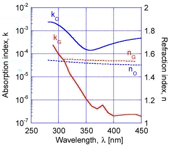
Figure 1.
Complex refraction index of the glass substrate (nG, kG) and organic layer (nO, kO).
The organic layers were coated on glass substrates using two methods: spin coating and inkjet printing. Prior to coating, glass substrates were washed with acetone and isopropyl alcohol and then rinsed with deionized water. Spin coating was applied to a 24 × 24 mm2 glass substrate at spin speeds ranging from 700 rpm to 4500 rpm, resulting in six different thicknesses of the organic layer. The organic layers were also coated on glass substrates using inkjet printing, covering an area of 20 × 20 mm2 with varying thicknesses. The inkjet printing system consists of dual print heads, each of which has 1776 (296 × 6 rows) nozzles arranged at 600 npi, to achieve a printing resolution of 1200 dpi with a drop volume of 4.2 pL per nozzle. The printing speed and the number of overlapping prints were fixed by 200 mm/s and five times, respectively, and the thickness of the printing layer was adjusted by varying the printing density through a dither-based halftoning method [23].
2.2. Light Extinction Measurement
Figure 2 illustrates the light extinction of a single glass layer and a glass-organic bilayer. The extinction of vertically incident light in a single layer can be described by the light absorption in the glass and the reflection at the glass–air interfaces as functions of the absorption coefficient of glass, αG = 4πkGλ−1, and the transmittance at the surface of glass in the air, TG, respectively.
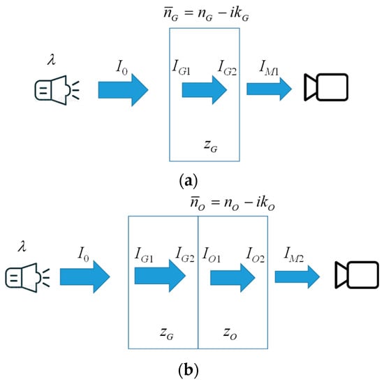
Figure 2.
Light intensities through (a) a single glass layer and (b) a glass-organic bilayer.
Here, zG is the thickness of the glass substrate, I0 is the intensity of incident light, IG1 and IG2 are the intensities of light in the glass at the front and the back surfaces, and IM1 is the measured light intensity, respectively. Since glass is transparent (kG << 1) for the measuring wavelength, λ = 300 nm, TG can be estimated by Equation (3).
Similarly, for the glass-organic bilayer, the light intensities can be correlated as follows:
where
Here, zO is the thickness of the organic layer, IO1 and IO2 are the intensities of light in the organic layer at the front and the back surfaces, IM2 is the intensity of light measured after passing through the bilayer, TO is the absorption coefficient of the organic layer, TOG is the transmittance at the interface of glass and the organic layer, and TO is the transmittance at the surface of the organic layer, respectively. From the refractive index in Figure 1 and Equation (7), the effective absorption coefficient, TO, was 0.08 μm−1 for a wavelength of 300 ± 5 nm.
As shown in Figure 1, a well-made optically clear resin has nearly the same refractive index as glass (nO = nG), and it is highly transparent (kO << nO). Therefore, TOG and TO can be simplified as follows:
From Equations (2) and (4)–(6), the distribution of the organic layer thickness, zO, can be obtained by calculating the intensity ratio between the light after passing through the bare glass, IM1, and the light after passing through the glass coated with the organic layer, IM2.
Figure 3 shows the schematic of the light extinction measurement system. The setup consists of a 300 nm wavelength light source (M300L4, THORLABS, Newton, NJ, USA), a collimator for producing parallel light, a 5× objective lens, and a CCD camera (pco.ultraviolet, Excelitas, Waltham, MA, USA) with 1392 × 1040 pixels and a 300 ± 5 nm bandpass filter, enabling a measurement range of 4872 × 3640 μm2 with an XY resolution of 3.5 μm. The typical images of the measured intensity of light extinction for a glass substrate, IM1, and an organic layer spin-coated glass substrate at 1500 rpm, IM2, are shown in Figure 4a and Figure 4b, respectively. Figure 4c displays the intensity ratio of IM2/IM1. In this figure, all the light intensities are relative values to the average intensity of the bare glass substrate, IM1,avg, over the measured area. Figure 5 shows the root mean squared error (RMSE) between the measurements. It can be clearly seen that the RMSE could be reduced to the level of several nanometers by pixel binning and image overlaying. By overlaying 16 images for each measurement, the current light extinction method was able to achieve an RMSE of less than 30 nm (0.75%) without pixel binning.
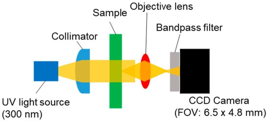
Figure 3.
Schematic of the light extinction image measurement system.
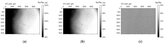
Figure 4.
Relative intensity of the light measured through (a) a glass substrate, IM1/IM1,avg, (b) an organic layer spin-coated glass substrate with 1500 rpm, IM2/IM1,avg, and (c) the ratio of IM2/IM1.
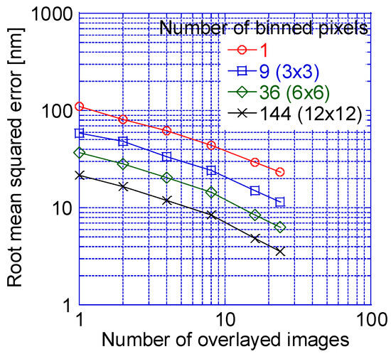
Figure 5.
Variation in the root mean squared error of the light extinction-based thickness measurements as a function of pixel binning and image overlay.
Figure 6 and Figure 7 compare the thickness measurements obtained using the light extinction image method with those from the FIB-SEM method (Helios 5 UX, Thermo Fisher, Waltham, MA, USA). Despite being a point measurement method and a destructive method, SEM has been adopted as a comparative method because it is the most accurate and is specified in the Thickness Measurement Standard (SPS-KION002-6253) [24]. The distinct difference between the two methods is not only whether the sample is destroyed but also the measurement dimension and the measurement area that can be measured at once: the thickness profile provided by the FIB-SEM is one-dimensional, and the length of the measurement area is inevitably on the same scale as the thickness. In contrast, light extinction can provide two-dimensional profiles, and the length scale of the measurement area can be extended regardless of the thickness scale. As shown in Figure 6, for example, when measuring an organic layer spin-coated at 2000 rpm, the FIB-SEM images provide cross-sectional thickness profiles over a transverse range of 17 μm, while the light extinction image provides a 2D profile over an area of 4872 × 3640 μm2. The average thickness, zO,avg, measured by the light extinction image could be easily obtained from individual pixel data.
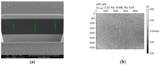
Figure 6.
Thickness profiles of the organic layer spin-coated with 2000 rpm: (a) cross-sectional profile measured by an FIB-SEM image; (b) 2D profile measured by a light extinction image.
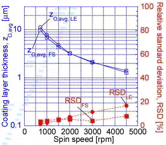
Figure 7.
Variation in average thickness, zO,avg, and relative standard deviation, RSD, of the spin-coated organic layer as a function of spin speed, measured by FIB-SEM (FS) and light extinction (LE) methods.
Figure 7 shows the variation in the average thickness, zO,avg and its relative standard deviation, RSD, of the spin-coated organic layer as a function of spin speed, indicating a strong agreement between the FIB-SEM (FS) method and the light extinction (LE) method. Here, for the SEM measurements, each average thickness and standard deviation are the results of data from 27 measurement points in nine images obtained from different locations.
Of course, there are some limitations to consider when using this measurement method. (1) If there are multiple layers of unknown thickness distribution, multiple light sources with different wavelengths are needed to measure the thickness of each layer. (2) If any of the layers are opaque to either of the lights, the thickness of any layer cannot be measured. (3) If any of the layer contains nonuniformly dispersed particles or particles larger than the wavelength, the measured thickness cannot be accurate. (4) If the thickness of the layer is much smaller than the absorption coefficient, the signal-to-noise ratio for this measurement decreases, making it less practical.
3. Results
3.1. Measurement of Thickness Uniformity
Figure 8 displays thickness distribution images of spin-coated organic layers at various spin speeds in the central region of the substrate. The images are visually represented on a gray scale ranging from −0.4 μm to +0.4 μm, centered on the average thickness. From 1,447,680 data points of the 4872 × 3640 μm2 area obtained from each measurement, the arithmetic average, Ra, and root mean square average, Rq, of the roughness profiles were also calculated using Equations (12) and (13), respectively.
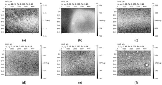
Figure 8.
Distribution of organic layer thickness, zO, spin-coated at (a) 700 rpm, (b) 1000 rpm, (c) 1500 rpm, (d) 2000 rpm, (e) 3000 rpm, and (f) 4500 rpm.
As the spin speed increases from 700 rpm to 4500 rpm, reducing zO,avg from 11.25 μm to 1.41 μm, Ra slightly decreases from 0.088 μm to 0.068 μm. However, Rq increases from 0.16 μm to 0.24 μm, indicating that the surface waviness increases with spin speed. As we can see in Figure 8, wavy nonuniformities of circular and linear shapes can be intuitively observed from these images at a glance. The results demonstrate that this light extinction-based measurement can be actively utilized not only for surface roughness evaluation but also for surface waviness observations of spin-coated and inkjet-printed organic layers on transparent substrates.
In Figure 9, the thickness distribution of the inkjet-printed organic layer is shown for printing densities of 40%, 60%, and 80%. In this case, the printing direction is from left to right, and a longitudinal waviness perpendicular to the printing direction that becomes more pronounced with printing density is observed. As the printing density increases from 40% to 80%, zO,avg increases proportionally from 6.63 μm to 12.73 μm. Unlike spin coating, both Ra and Rq also increase linearly from 0.056 μm to 0.084 μm and from 0.073 μm to 0.11 μm, respectively.
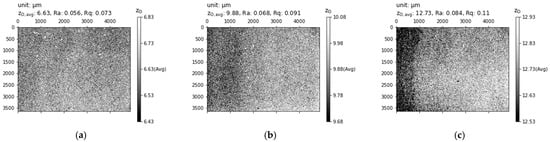
Figure 9.
Distribution of organic layer thickness, zO, inkjet-printed at printing densities of (a) 40%, (b) 60%, and (c) 80%. Printing direction is from left to right.
The surface roughness characteristics of the organic layer were compared using spin coating and inkjet printing methods, as shown in Figure 10. In the figure, blue solid symbols and red hollow symbols represent Ra and Rq, respectively, while circles and squares represent spin coating and inkjet printing, respectively. As shown in Figure 10, Ra, which evaluates the smoothness of the surface, does not show a significant difference between inkjet printing and spin coating. However, Rq, which evaluates the flatness of the surface, shows a significant difference between them. Quantitatively, the Rq of the inkjet-printed layer is significantly smaller than that of the spin-coated layer. Moreover, qualitatively, the Rq of the inkjet-printed layer decreases as the layer thickness decreases, while the Rq of the spin-coated layer tends to increase as the thickness decreases. These results imply that the inkjet printing method is relatively advantageous for forming a thin and uniform film.
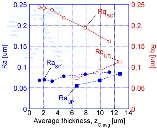
Figure 10.
Variation in arithmetic average, Ra, and root mean square average, Rq, of surface roughness for spin-coated (SC) and inkjet-printed (IJP) organic layers, as a function of average thickness, zO,avg.
3.2. Observation of Edge Beads
Figure 11 shows the thickness distribution of the spin-coated organic layer near the edge of the substrate for various spin speeds ranging from 700 rpm to 4500 rpm. Figure 11a shows thickness distribution images measured by the light extinction method, where the edges of the layers are located on the left side of the images, and the center direction is on the right side of the images. In the images, the thickness of the bright area is higher, and the median brightness level was adjusted to the average thickness, zO,avg, of each layer. Figure 11b shows the thickness profiles along the a-a’ cross-sections of the images in Figure 11a. As shown in Figure 11, the light extinction image method successfully measured thickness distributions that vary significantly near the edge. This method clearly captured the typical edge beads produced during spin coating [25,26]. In this figure, the height and width of the edge bead decrease with spin speed.
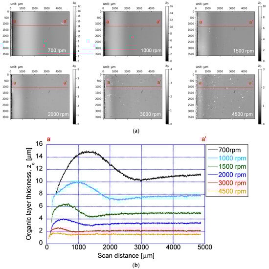
Figure 11.
Thickness distribution of spin-coated organic layer near the edge of the substrate for various spin speeds from 700 rpm to 4500 rpm: (a) 2D distribution; (b) cross-sectional profiles along a-a’.
The thickness distribution of the inkjet-printed organic layer near the pattern edge was also shown for various printing densities in Figure 12. A ridge shape similar to the edge bead formed by spin coating is observed at the edge of the inkjet-printed organic layer [14], which is caused by the surface tension of the ink at the edge. Interestingly, in inkjet printing, the thickness distribution image of the edge bead region remains very similar regardless of changes in thickness due to printing density. This suggests that, unlike spin coating, the ratio of edge bead height to average thickness does not vary significantly with changes in thickness.
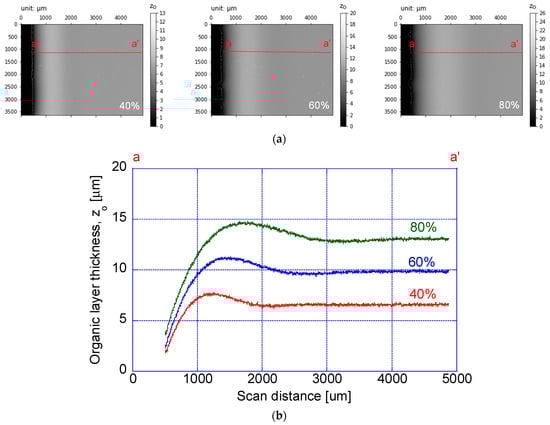
Figure 12.
Thickness distribution of inkjet-printed organic layer near the edge of the printed pattern for various printing densities of 40%, 60%, and 80%: (a) 2D distribution; (b) cross-sectional profiles along a-a’.
Figure 13 compares the change in edge bead height according to the average layer thickness, zO,avg, for two coating techniques: spin coating and inkjet printing. Here, the height of the edge bead, δ, was defined as follows:
where zO,max is the maximum thickness at the ridge. It can be seen that the bead height increases as the thickness increases, and the bead height of inkjet printing is lower than that of spin coating when the thickness is high. For spin coating, as shown in Figure 13, δ increases from 0.32 μm to 3.60 μm with decreasing spin speed, while the average layer thickness, zO,avg, increases from 1.41 μm to 11.25 μm. This results in an increase in the relative height of δ/zO,avg from 23% to 32%. On the other hand, δ, made by inkjet printing, was measured to be 1.33 μm, 1.97 μm, and 2.88 μm for zO,avg of 6.63 μm, 9.88 μm, and 12.73 μm, so that the relative heights, δ/zO,avg, of the corresponding inkjet-printed layers did not vary significantly with the thickness change, being 20.1%, 19.9%, and 22.6%, respectively.
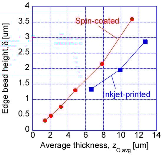
Figure 13.
Variation in edge bead height, δ, formed by spin coating and inkjet printing as a function of average thickness, zO,avg.
Finally, Figure 14 shows the overall distribution along the printing direction for a printing density of 60%, which was created by connecting successively measured light extinction images. In this figure, the cross-sectional profile measured by the light extinction was also compared to that measured by a surface profiler (P-7, KLA-Tencor, Milpitas, CA, USA), showing that the two results are in good agreement.
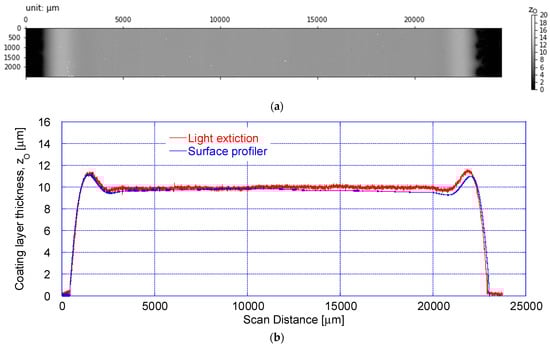
Figure 14.
Edge-to-edge thickness distribution of inkjet-printed organic layer for printing density of 60%: (a) 2D distribution measured by the light extinction method; (b) cross-sectional profiles along the printing direction (from left to right) measured by the light extinction method and a surface profiler.
4. Conclusions
Two-dimensional thickness distributions of organic microlayers on glass substrates, which are used in optically transparent resin for displays and thin film encapsulation for flexible OLEDs, were quantitatively and qualitatively measured using a UV light extinction imaging method. Quantitatively, the organic materials tested absorbed 40 to 50% of light with a wavelength of 300 nm through a layer with a thickness of 3 to 4 μm. Consequently, a measurement error of less than a few nanometers could be achieved through image overlay and pixel binning. Qualitatively, this non-destructive, non-contact, two-dimensional measurement method enables immediate and intuitive analysis of the thickness distribution or surface waviness of the coated layer.
This UV light extinction imaging method was applied to comparatively evaluate the characteristics of spin-coated and inkjet-printed organic layers. The thickness uniformity of the inkjet-printed layer was found to be superior to that of the spin-coated layer in the central area of the coating. In particular, the difference became more evident as the layer thickness decreased. This was observed as the root mean square average of the surface roughness of the inkjet-printed layer decreased with thinner layers, while it increased for the spin-coated layer. At the edge of the coating, edge beads with increased thicknesses were commonly observed. However, unlike spin coating, where the edge bead height relatively shrinks as the layer thickness decreases, the edge bead height of the inkjet-printed layer remained at approximately 20% of the average layer thickness regardless of changes in layer thickness.
Author Contributions
Conceptualization, J.Y.H.; methodology, J.H.Y., H.T.K., G.-Y.Y. and J.H.K.; software, J.H.Y.; validation, H.T.K., D.W.L. and S.W.L.; formal analysis, J.Y.H.; investigation, J.H.Y., G.-Y.Y. and J.Y.H.; resources, H.T.K., D.W.L. and S.W.L.; writing—original draft preparation, J.H.Y.; writing—review and editing, J.Y.H. All authors have read and agreed to the published version of the manuscript.
Funding
This study was supported by the Industry Technology R&D Program as “Development of Organic Thin Film Encapsulation Equipment (20016124)” funded by the Ministry of Trade, Industry & Energy (MOTIE, South Korea).
Institutional Review Board Statement
Not applicable.
Informed Consent Statement
Not applicable.
Data Availability Statement
Data are contained within the article.
Conflicts of Interest
All authors have no conflicts of interest.
References
- Kim, Y.-G.; Park, B.-M.; Choi, J.-K.; Jang, D.-H.; Han, K.-Y. Optimization of the Rework of Bended OLED Displays by Surface-Energy Control. Coatings 2021, 11, 1523. [Google Scholar] [CrossRef]
- Tan, G.; Lee, J.-H.; Lan, Y.-H.; Wei, M.-K.; Peng, L.-H.; Cheng, I.-C.; Wu, S.-T. Broadband antireflection film with moth-eye-like structure for flexible display applications. Optica 2017, 4, 678–683. [Google Scholar] [CrossRef]
- Grego, S.; Lewis, J.; Vick, E.; Temple, D. evelopment and evaluation of bend-testing techniques for flexible-display applications. J. Soc. Inf. Disp. 2005, 13, 575–581. [Google Scholar] [CrossRef]
- Jeong, E.G.; Kwon, J.H.; Kang, K.S.; Jeong, S.Y.; Choi, K.C. A review of highly reliable flexible encapsulation technologies towards rollable and foldable OLEDs. J. Inf. Disp. 2020, 21, 19–31. [Google Scholar] [CrossRef]
- Chen, X.; Liu, B.; Zhong, C.; Liu, Z.; Liu, J.; Ma, L.; Deng, Y.; Han, X.; Wu, T.; Hu, W.; et al. Ultrathin Co3O4 Layers with Large Contact Area on Carbon Fibers as High-Performance Electrode for Flexible Zinc–Air Battery Integrated with Flexible Display. Adv. Energy Mater. 2017, 7, 1700179. [Google Scholar] [CrossRef]
- Zhang, H.; Ding, H.; Wei, M.; Li, C.; Wei, B.; Zhang, J. Thin film encapsulation for organic light-emitting diodes using inorganic/organic hybrid layers by atomic layer deposition. Nanoscale Res. Lett. 2015, 10, 169. [Google Scholar] [CrossRef] [PubMed]
- Li, Y.; Xiong, Y.; Yang, H.; Cao, K.; Chen, R. Thin film encapsulation for the organic light-emitting diodes display via atomic layer deposition. J. Mater. Res. 2020, 35, 681–700. [Google Scholar] [CrossRef]
- Kwon, J.H.; Choi, S.; Jeon, Y.; Kim, H.; Chang, K.S.; Choi, K.C. Functional design of dielectric–metal–dielectric-based thin-film encapsulation with heat transfer and flexibility for flexible displays. ACS Appl. Mater. Interfaces 2017, 9, 27061–27072. [Google Scholar] [CrossRef] [PubMed]
- Houbertz, R.; Domann, G.; Cronauer, C.; Schmitt, A.; Martin, H.; Park, J.-U.; Frohlich, L.; Buestrich, R.; Popall, M.; Streppel, U.; et al. Inorganic–organic hybrid materials for application in optical devices. Thin Solid Films 2003, 442, 194–200. [Google Scholar] [CrossRef]
- Kim, Y.-G.; Park, B.-M.; Han, K.-Y. A study on the spreading characteristics of OCR lamination for flexible OLED. Jpn. J. Appl. Phys. 2020, 59, 080901. [Google Scholar] [CrossRef]
- Yu, D.; Yang, Y.-Q.; Chen, Z.; Tao, Y.; Liu, Y.-F. Recent progress on thin-film encapsulation technologies for organic electronic devices. Opt. Commun. 2016, 362, 43–49. [Google Scholar] [CrossRef]
- Kwon, B.-H.; Joo, C.W.; Cho, H.; Kang, C.; Yang, J.-H.; Shin, J.-W.; Kim, G.H.; Choi, S.; Nam, S.; Kim, K.; et al. Organic/Inorganic Hybrid Thin-Film Encapsulation Using Inkjet Printing and PEALD for Industrial Large-Area Process Suitability and Flexible OLED Application. ACS Appl. Mater. Interfaces 2021, 13, 55391–55402. [Google Scholar] [CrossRef] [PubMed]
- Lee, S.; Han, J.-H.; Lee, S.-H.; Baek, G.-H.; Park, J.-S. Review of Organic/Inorganic Thin Film Encapsulation by Atomic Layer Deposition for a Flexible OLED Display. J. Met. 2019, 71, 197–211. [Google Scholar] [CrossRef]
- Tehrani, B.K.; Mariotti, C.; Cook, B.S.; Roselli, L.; Tentzeris, M.M. Development, characterization, and processing of thin and thick inkjet-printed dielectric films. Org. Electron. 2016, 29, 135–141. [Google Scholar] [CrossRef]
- Xing, R.; Ye, T.; Ding, Y.; Ding, Z.; Ma, D.; Han, Y. Thickness Uniformity Adjustment of Inkjet Printed Light-emitting Polymer Films by Solvent Mixture. Chin. J. Chem. 2013, 31, 1449–1454. [Google Scholar] [CrossRef]
- Zhu, Z.; Ning, H.; Cai, W.; Wei, J.; Zhou, S.; Yao, R.; Lu, X.; Zhang, J.; Zhou, Z.W.; Peng, J. Morphology modulation of direct inkjet printing by incorporating polymers and surfactants into a sol–gel ink system. Langmuir 2018, 34, 6413–6419. [Google Scholar] [CrossRef]
- Giurlani, W.; Berretti, E.; Innocenti, M.; Lavacchi, A. Measuring the thickness of metal films: A selection guide to the most suitable technique. Mater. Proc. 2020, 2, 12. [Google Scholar] [CrossRef]
- Gao, F.; Muhamedsalih, H.; Jiang, X. Surface and thickness measurement of a transparent film using wavelength scanning interferometry. Opt. Express 2012, 20, 21450–21456. [Google Scholar] [CrossRef]
- Nestler, P.; Helm, C.A. Determination of refractive index and layer thickness of nm-thin films via ellipsometry. Opt. Express 2017, 25, 27077–27085. [Google Scholar] [CrossRef]
- Sokolov, V.I.; Marusin, N.V.; Panchenko, V.Y.; Savelyev, A.G.; Seminogov, V.N.; Khaydukov, E.V. Determination of refractive index, extinction coefficient and thickness of thin films by the method of waveguide mode excitation. Quantum Electron. 2013, 43, 1149–1153. [Google Scholar] [CrossRef]
- McGahan, W.A.; Johs, B.; Woollam, J.A. Techniques for ellipsometric measurement of the thickness and optical constants of thin absorbing films. Thin Solid Films 1993, 234, 443–446. [Google Scholar] [CrossRef]
- Qin, Z.; Liu, Q.; Yue, C.; Lang, Y.; Zhou, X. Nanoscale film thickness measurement based on weak measurement. Rev. Sci. Instrum. 2020, 91, 123111. [Google Scholar] [CrossRef] [PubMed]
- Ostromoukhov, V.; Emmel, P.; Rudaz, N.; Amidror, I.; Hersc, R.D. Dithering algorithms for variable dot size printers. In Proceedings of the 3rd IEEE International Conference on Image Processing, Lausanne, Switzerland, 16–19 September 1996; pp. 553–556. [Google Scholar]
- SPS-KION002-6253; Measurement of Multi-Layer Thickness under 200 nm Scanning Electron Microscope Method. Korea Infrastructure Organization for Nanotechnology: Seoul, Republic of Korea, 2015.
- Baëtens, T.; Arscott, S. Planarization and edge bead reduction of spin-coated polydimethylsiloxane. J. Micromech. Microeng. 2019, 29, 115005. [Google Scholar] [CrossRef]
- Yan, Y.; Li, J.; Liu, Q.; Zhou, P. Evaporation effect on thickness distribution for spin-coated films on rectangular and circular substrates. Coatings 2021, 11, 1322. [Google Scholar] [CrossRef]
Disclaimer/Publisher’s Note: The statements, opinions and data contained in all publications are solely those of the individual author(s) and contributor(s) and not of MDPI and/or the editor(s). MDPI and/or the editor(s) disclaim responsibility for any injury to people or property resulting from any ideas, methods, instructions or products referred to in the content. |
© 2024 by the authors. Licensee MDPI, Basel, Switzerland. This article is an open access article distributed under the terms and conditions of the Creative Commons Attribution (CC BY) license (https://creativecommons.org/licenses/by/4.0/).