Article

Rate-Dependent Evolution of Microstructure and Stress in Silicon Films Deposited by Electron Beam Evaporation

by
Runar Plünnecke Dahl-Hansen
*,
Marit Stange
,
Tor Olav Sunde
and
Alexander Ulyashin
SINTEF, Forskningsveien 1, 0373 Oslo, Norway
*
Author to whom correspondence should be addressed.
Coatings 2024, 14(7), 808; https://doi.org/10.3390/coatings14070808
Submission received: 31 May 2024 / Revised: 24 June 2024 / Accepted: 26 June 2024 / Published: 28 June 2024

Abstract

:
Growing high-quality Si films at high rates with thicknesses ranging from the few nm- to µm-range while keeping the material consumption at a minimum is important for a wide range of Si-based technologies, spanning from batteries to sensors and solar cells. In this work, we elucidate the effects of electron beam deposition (e-beam) conditions on the growth of ~4 µm thick Si layers on bare and thermally oxidized (001)-oriented Si substrates. All depositions are performed from a stabilized and refillable melt of broken B-doped wafers and recollected using Si-shields during deposition for recycling. We find that increasing the deposition rate from 0.3 to 23 nm/s at a substrate temperature of 1000 °C reduces the roughness, void fraction, and residual stress of epitaxial Si-on-Si layers. For Si-on- S i O 2 , all films are polycrystalline under the same deposition conditions as for Si-on-Si, with a reduction in void fraction and increase in roughness at higher deposition rates. The residual stress for Si-on- S i O 2 is comparable across all deposition rates >1 nm/s. Furthermore, we measure lower resistivities in the films than in the feedstock for Si-on-Si and higher than the feedstock for Si-on- S i O 2 . While the films become microstructurally denser and less defective at higher deposition rates, the resistivity increases for each next deposition step in the case of multi-step depositions from the same feedstock. Time-of-flight scanning secondary mass spectroscopy measurements show that the films have a significantly higher B-concentration than the feedstock, suggesting B-gettering to the melted region and transferring to the Si film upon the e-beam deposition process. This work demonstrates how electron beam evaporation can be used to recollect and recycle waste Si pieces, bringing important insights into how the deposition parameters influence the quality of the deposited polycrystalline as well as epitaxial thin-to-thick films.

1. Introduction

Silicon (Si)-based technology encompasses essential applications ranging from photovoltaics (PV) [1] and batteries [2,3,4] to embedded electronics and photonics [5] and Si-based sensors [6,7,8,9]. Realizing new and improving established technologies requires depositing thin as well as thick Si layers using scalable methods with accurate microstructural control [10,11]. For instance, while defect-free thin and thick monocrystalline Si films are required for, e.g., PV and electronics, the ability to prepare porous silicon morphologies is advantageous for, e.g., silicon anodes for lithium-ion batteries. Si is currently in high demand (Now considered a critical raw material), which puts pressure on the environmental footprint, cost, and material consumption for Si-based technology [12]. The latter is a highlighted challenge with regards to the growing number of solar cell installations; as the solar energy capacity climbs towards ~8500 GW, so does the expected solar panel waste, projected to reach up to 78 million tons of waste by 2050 [13,14]. A “take-make-use-dispose” model raises large environmental concerns, pressing a need for innovative approaches to recover and recycle PV materials.
Recovering semiconductor materials with high purity is a considerable challenge. Depositing Si using electron-beam vapor deposition (e-beam) is a relatively simple approach compared to, e.g., plasma enhanced or low-pressure chemical vapor deposition (LPCVD, PECVD) and is interesting for several reasons: (i) it enables the deposition of thin-to-thick monocrystalline Si layers with deposition rates exceeding 1.5 µm/min [15,16], (ii) it does not require a complex infrastructure compared to, e.g., PECVD/LPCVD, and (iii) it opens up the possibility for e-beam refining and material recycling. In e-beam, deposition is carried out by melting a target Si-source in a vacuum using an electron beam and depositing the evaporated material flux onto a substrate. The source material, collected in a suitable crucible, can be Si pieces, kerf, or even scrap material, which makes e-beam an enabling technique to refine, remelt, and redeposit/recycle Si from various forms into high-quality Si layers. High-quality polycrystalline, as well as epitaxial layers with thicknesses from a few nm up to several hundred µm, can thus be achieved within the same relatively simple vacuum system. When deposited onto, e.g., a reusable template Si substrate, such layers can be released using thin-film transfer methods, such as etching or cold-cutting [17,18], and integrated with the relevant application. Being a “direct wafering” technique for thin to thick wafers, the method can substantially reduce material consumption and loss compared to conventional wafer growth using, e.g., Czochralski (CZ) or float-zone (FZ) methods. This is because e-beam does not suffer from physical limitations in the saw-to-wafer thickness ratio and does not leave behind Si kerf in the process, which, for thin wafers, can account for over 50% of the material usage.
Despite being an attractive deposition technique for thin and thick films, obtaining high-quality layers using e-beam is challenging and detrimental to its applicability and requires attention to the interplay between the deposited material, the substrate, and the deposition conditions. First, Si is a high-melting-point material with a relatively low surface adatom mobility and requires relatively high substrate temperatures to achieve high-quality layers [15]. Second, the substrate properties, on the other hand, and particularly the crystallographic orientation, surface roughness, and cleanliness, affect the initial stages of growth and dictate the subsequent deposition. Third, accurately controlling the deposition conditions, such as the vacuum level, ambient species, and material flux, is imperative to reduce the number and extension of microstructural defects protruding from the film. While the previous work [15,16] demonstrated that epitaxial wafer-level films can indeed be achieved using e-beam, achieving applicable high-quality films requires a deeper understanding of the connection between the deposition conditions and the film properties.
In this work, we demonstrate a system for recollecting and depositing Si at different rates on large-scale 6” Si substrates by e-beam. Polycrystalline and epitaxial films are obtained through tuning the deposition conditions. To obtain an improved understanding of the interrelation between the substrate, film, and deposition conditions, the focus is on how the film’s microstructure, mechanical stress, and resistivity evolve for varying deposition conditions on two substrates of interest: (001)-oriented, Si with and without 1 µm thermally grown S i O 2 . We show how the microstructural features and physical properties of the deposited film depend on the substrate and deposition rate, r d , and connect with the residual stress of the film. While high residual stresses can induce mechanical failures detrimental to thin-film devices, such as substrate bending, film cracking, and delamination, it also gives valuable insights into the kinetic processes occurring during growth.

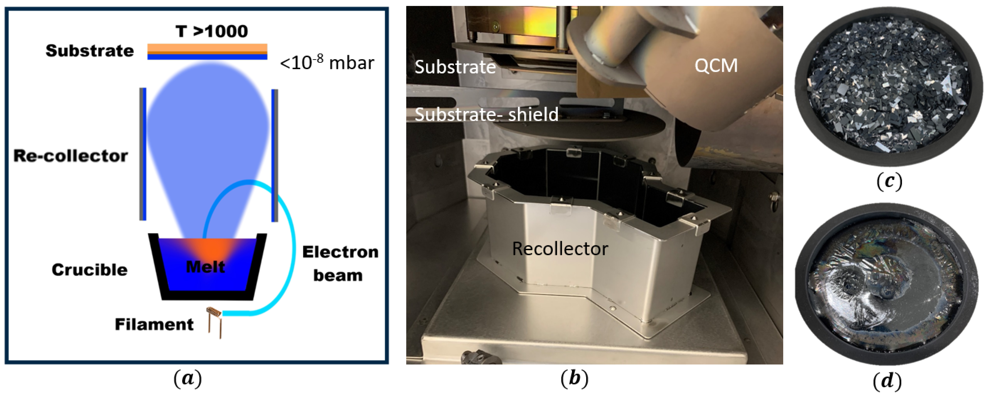
2. Materials and Methods
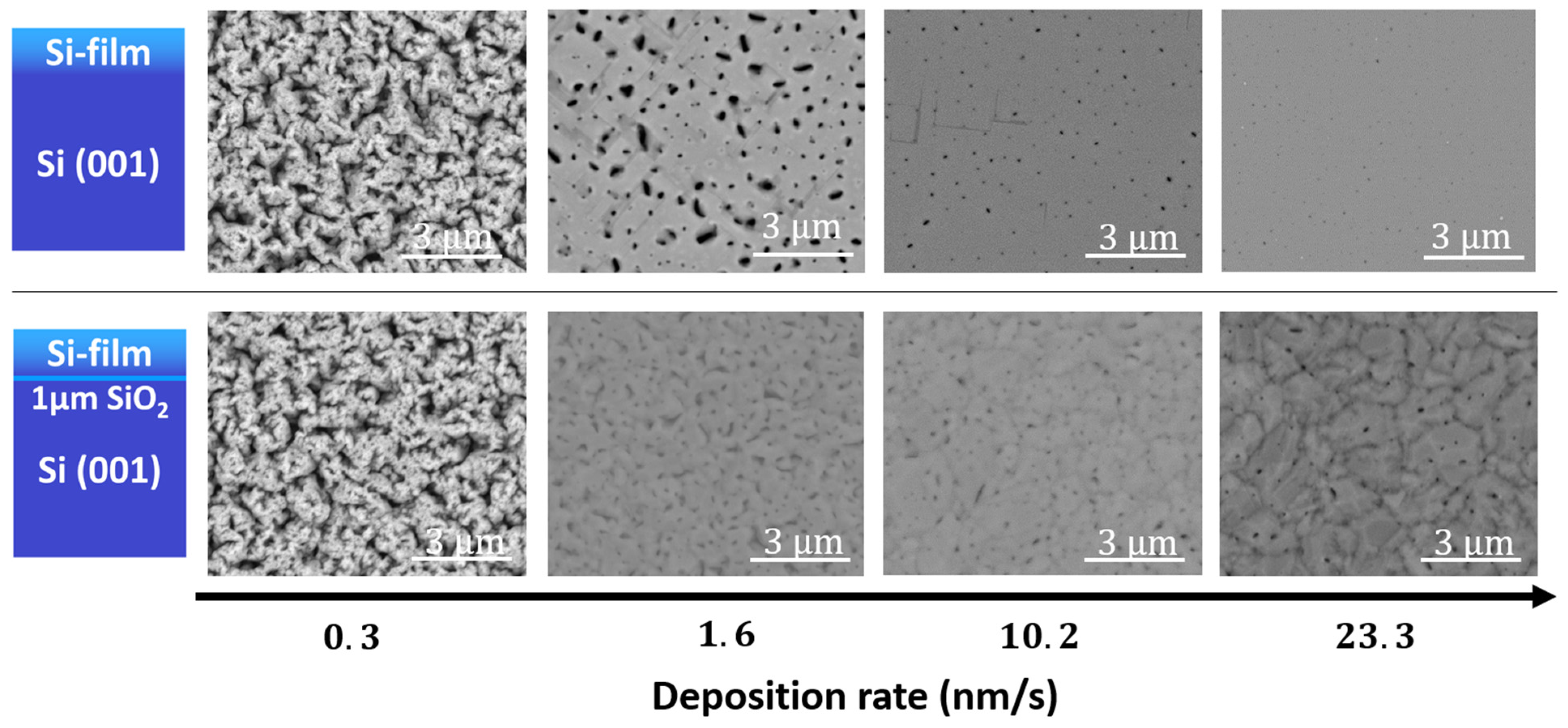
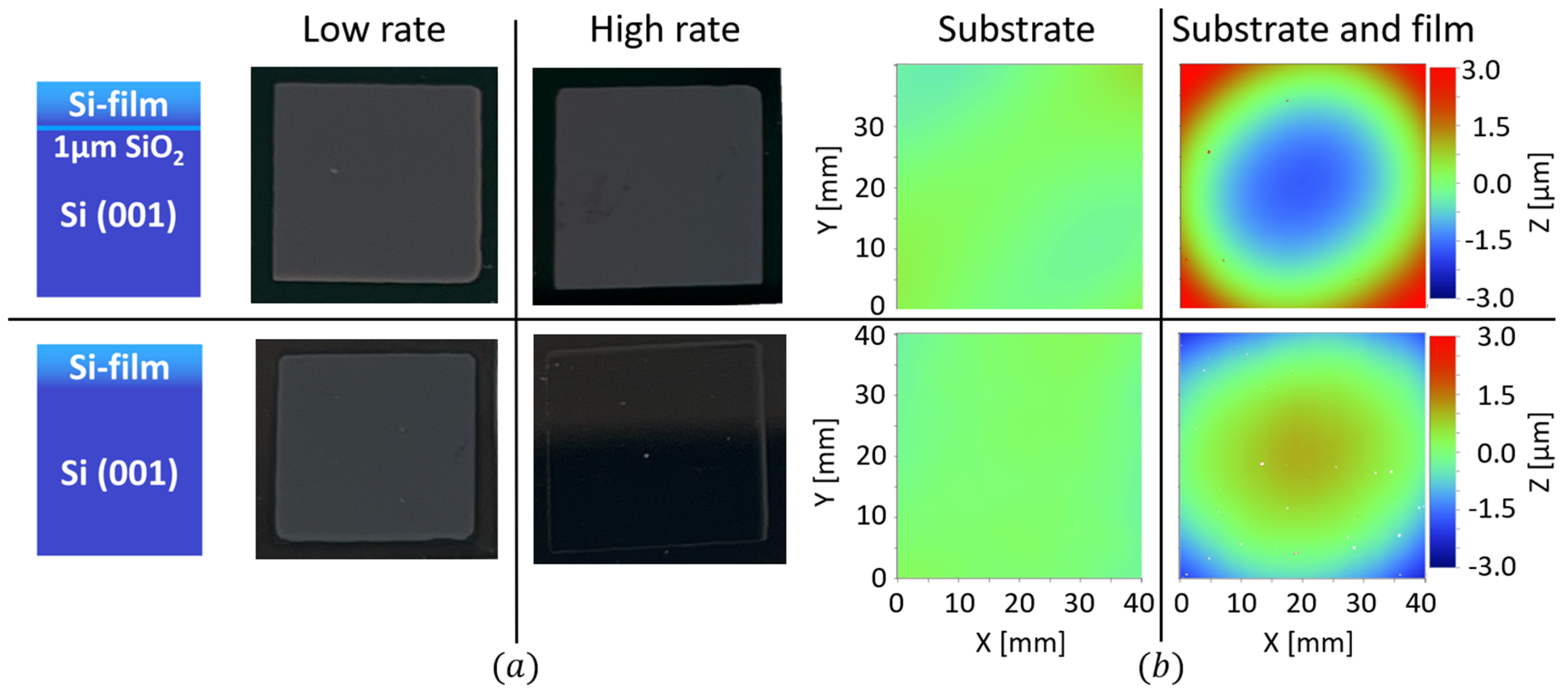
Figure 1 shows a schematic (a) and an image of the experimental setup used here (b). A combination of permanent magnets and electromagnets steers the electron beam emitted from the W-filament into the crucible. Then, 130 µm thick Si tightly fit liners surrounding the crucible recollect the non-directional Si material flux from the melt, not deposited onto the substrate. The initial feedstock, comprising broken pieces of Boron-doped solar grade (SOG) Si with a nominal doping concentration of 2.7 × 10 15 atomic Boron/ c m 3 and resistivity ρ s o u r c e = 5.5 5.7 · c m , is the same material (in the form of non-broken Si wafers) used for recollection liners. The SOG Si was received from the industrial partner—Norwegian company Norsun. After each crucible refill, a melt stabilization procedure of 15 min initial low-power remelting, followed by a 15 min melt stabilization, is carried out to ensure stable, reproducible deposition conditions. A freshly refilled and stabilized melt is shown in Figure 1c and Figure 1d, respectively.
Ten experiments, termed Si1–Si10, were performed, increasing the deposition rate, r d , in every consecutive deposition. All the films were deposited using a Polyteknik Flextura 200 cluster system with a base pressure below 1 × 10 8 mbar. First, 4.3 ± 0.5 µm thick Si layers were evaporated from a 500 c m 3 Si source onto 10 × 10 mm2 and 50 × 50 mm2 675 µm thick (001)-oriented Si substrates. The smaller substrates were laser-diced (Rofin PL E 25 SHG CL Flex, Coherent Inc.) from 6” single-side polished phosphorous-doped n-type float zone wafers (Siegert Wafer GmbH) with a resistivity of 3–7 k Ω · c m .
The deposited layer thickness was measured by white light interferometry (WLI, WYKO NT9800, Bruker Corp.) at the step-edge defined by the substrate holder. The measured thicknesses are tabulated in Table A1 of Appendix A. All pure Si-substrates were etched in 1% hydrofluoric (HF) acid for 1 min before loading into a load–lock chamber, reaching < 10 5 mbar within 10 min after etching. Since HF removes oxides, the Si wafers with 1 µm S i O 2 thermally grown at 1050 °C in an O 2 ambient, were ultrasonically cleaned in acetone, isopropanol, and deionized water for 5 min each step before loading. Measured across the 1 µm thick layer, ρ S i O 2   >   100 E Ω · c m below 30 V. This corresponds to a current range of ~50 pA, indicating that the oxide is a high-quality insulator. After the substrate is loaded into the deposition chamber, a reducing background pressure is applied by flushing the chamber with a flow of 0.4 sccm H 2 (g) throughout the entire experiment.
The substrate temperature, T S , is stabilized during the flushing step and kept at 1025 ± 25 °C for all depositions. The r d of 0.2 23.5 nm/s is controlled by an e-beam emission current of 150–650 mA, using a gold-coated 6 MHz crystal-quartz microbalance (QCM, Inficon Holdin AG) monitor as a feedback loop. The source rotates at a constant speed of 0.1 rpm to melt as large an area as possible, while the e-beam has a 20 mm peak-to-peak off-centered linear scanning pattern. Two consecutive power-ramping sequences, each with a ramp rate of 0.5 mA/s and soaking for 150 s with a 150 mA increment in emission current per step, stabilize the melt before ramping up the power required for stabilizing r d . The deposition pressure never exceeded 10−5 mbar during deposition. Microstructural characterization was performed using scanning electron microscopy (SEM, FEI NOVA NanoSEM650, Thermo Fisher Scientific) for morphology. From the SEM images, ImageJ was used to analyze and extract microstructural features, hereunder defining a void fraction, V f %, as the percentage of the image covered by voids and a void area, A V   µ m 2 , as the average area of the voids within the image. A void is defined as a dark region within which a low SEM signal is detected during SEM acquisition. X-ray diffraction (XRD, Bruker AXS D8 Discover system, Bruker AXS GmbH) using Cu Kα1 radiation (λ = 1.54 Å) scanned over the angles 2θ = 20° to 80°) for crystallinity. In all cases, the Cu K alpha also sees the substrates. This, since the penetration depth of Cu K alpha in silicon is between 10–50 µm, depending on the 2theta angle, more than 50% of the XRD signal comes from the Si wafer. This reduces the sensitivity for weak peaks coming from the film. All deposited films were significantly thinner than the substrate so that the biaxial residual film stress could be estimated using Stoney’s equation [19]:
σ = M t S 2 6 t f 1 R 1 R 0
where M is the biaxial modulus of the substrate; M S i 001 = 1 s 11 S i + s 12 S i = 180.3 G P a and M S i 111 = 6 4 s 11 S i + 8 s 12 S i + S i 44 S i = 229.1 G P a for Si(001) and Si(111). t S = 650 ± µ m and t f t S are the thickness of the substrate and film, respectively, R 0 is the radius of curvature of the substrate, and R is the radius of curvature of the film-substrate system after deposition. R and R 0 were measured using WLI before and after deposition [20]. At the same time, WLI is used to measure the surface roughness across the substrates, which is compared with the microscopic surface roughness measured by atomic force microscopy (AFM), i.e., after measuring curvature, the background macroscopic bending is subtracted from the image, and the image is divided into 10 × 10 mm2 regions, in which the root mean square of heights is calculated by
R q = 1 n i = 1 n Z i Z ¯ 2
where Z i is the vertical height of grain i and Z ¯ is the average grain height.
The resistivity was measured using four-point probing (Jandel RM3-AR, Jandel Eng. Ltd.) on the template wafers with and without films and compared to the reference source of the melt. The Hall effect measurements were carried out using a Lakeshore 7605 (Lake Shore Cryotronics, Inc.) setup with soldered indium contacts. Lastly, scanning secondary ion mass spectroscopy (SIMS, Cameca IMS 7f microanalyzer, AMETEK, Inc.) was used to measure the Boron content of the fabricated films, indicating the degree of dopant melt-to-substrate transfer rate.

3. Results

Figure 2 shows XRD data for three selected r d , representing “low”, “medium”, and “high” rates for films on Si (a) and S i O 2 (b). The corresponding average rate is shown in the figure legend. The measurement of the relevant substrate is included as a reference. The occurrence of the basis-forbidden Si(200) reflection 2q = 33° (marked with ‘) is caused by multiple diffraction. The remaining low-intensity peaks, labeled with (*), are reflections from the sample stage. In Figure 2a, the high-intensity Si(400) reflection at 2θ = 69° and the absence of diffraction peaks from other crystallographic orientations in the XRD patterns confirms that the silicon films deposited on (100)-oriented wafers grow epitaxially in the (100) direction. This was true across all deposition rates. We also show in Appendix A that the films grow epitaxially also on (111)-oriented Si.
The films deposited on S i O 2 have a preferred (100)-orientation at low deposition rates, while additional peaks such as Si(131) and Si(133) appear at 10.2 and 23.3 nm/s, which confirms the polycrystalline nature of these films.
Figure 3 shows SEM images of films grown on Si (upper row) and S i O 2 (lower row) for low to high deposition rates. Below r d < 1 nm/s, the films have similar microstructural features independent of the host substrate. Fully crystalline films grew for all r d > 1 nm/s, with a significant reduction in extended defects as the r d increases. Whereas grains coalesce to a finer monocrystalline film on Si, the films remain polycrystalline on S i O 2 , with the grain sizes increasing with increasing r d . For both substrates, the void fraction and the number of crystallographic defects decrease with increasing r d . This is quantified and discussed below.
Figure 4 compares key general aspects of the films deposited on Si and S i O 2 . (a) shows pictograms of typical films deposited at high and low rates on 10 × 10 mm substrates, and (b) examples of measured curvatures by WLI before and after deposition. The latter is carried out within 40 × 40 mm2 of films deposited on 50 × 50 mm2 substrates, with corresponding residual stresses of 40.2 MPa (tensile) and −29.1 MPa (compressive), as highlighted in Figure 5d. Small spots in the pictograms show examples of spitting defects in the case of melt-through of the top surface layer during deposition. As indicated in (b), all substrates are initially relatively flat, measuring R 0 ~1000 m, and virtually free from extrinsic stress contribution. Though the thermal oxide has a compressive stress as-deposited of −300 MPa, the substrates are globally stress-neutral since the whole wafer is oxidized, front and back.
Table 1 and Figure 5 summarize the measured film characteristics for all depositions. Figure 5a shows measured roughness, R q , from WLI as a function of r d . The films deposited on S i O 2 measure a comparative R q as the one deposited on Si for r d < 1 nm/s, but the roughness increases with increasing r d . On the contrary, R q for the films deposited on Si is always lower and decreases by an order of magnitude with the increasing rate, reaching 2.7 nm at r d = 23.3 nm/s. In comparison, the initial roughness of the Si/ S i O 2 substrates were ~0.1 nm. For films deposited on both substrates, the void fraction from the SEM image analysis, Figure 5b, decreases exponentially with r d and is comparable in range for both substrates. Fits are shown in Appendix A. For R q v s . r d , only Si-on-Si displays an exponential decay, whereas Si-on- S i O 2 increases with r d .
Figure 5c shows resistivity vs. deposition rate. While the resistivity for Si-on-Si, ρ S i , is always lower than Si-on- S i O 2 , ρ S i O 2 , by 1–2 orders of magnitude, the films display the same trend on both substrates: ρ increase for every deposition and, therefore, for increasing deposition rates. ρ S i < ρ s o u r c e throughout all depositions, while ρ S i O 2 > ρ s o u r c e above 7 nm/s. The Hall effect measurements gave reliable and reproducible results only for Si-on-Si. The p-type Hall mobilities ranged from 47 to 124 cm2V−1s−1 for faster deposition rates. This correlates well with the microstructural evolution vs. r d , as seen in Figure 5a,b, displaying Hall mobilities close to that of crystalline silicon for solar cells [21]. For films deposited on S i O 2 , the Hall-effect experiments did not give reliable data.
Figure 5d shows the measured residual stress as a function of r d for Si-on-Si, σ S i and Si-on- S i O 2 , σ S i O 2 . The inset plots show the profile for the selected deposition, Si3, also marked in Figure 4. After film deposition, all Si-on-Si films are compressively stressed. σ S i relaxes with increasing r d , plateauing at approximately r d ~10 nm/s, and reaching a minimum of −6.7 MPa at r d = 23.3 nm/s. For Si-on- S i O 2 , σ S i O 2 > 0 (tensile stress) for all deposited films, reaching an apparent plateau at 2.3 nm/s, above which the measured stress does not significantly change.

4. Discussion

4.1. Microstructure Evolution

The substrate has significant implications on the film properties, largely dictating extended defect density [22,23]. Unit cell lattice matching is required for epitaxial layers to grow. In the case of a lattice mismatch, the film must epitaxially strain to match the substrate, resulting in strain energy building up with film thickness. Dislocation and favorable polycrystalline growth occur when the strain energy exceeds the film’s elastic energy, with this critical thickness decreasing as the lattice mismatch increases. With in-plane lattice constants a S i ~ 5.4 Å and a S i O 2 ~ 4.9 Å, the mismatch strain is 9.3%, meaning that the critical thickness will be in the nm range before polycrystalline growth is preferred. Thus, Si-on-Si grows epitaxially, and Si-on- S i O 2 has a polycrystalline (001)-preferred orientation, as shown in Figure 2.
For Si-on-Si, both the roughness and the void fraction decrease exponentially with the increasing deposition rate, r d . This trend can be rationalized by Si having a low adatom mobility, requiring a higher material influx to fill in voids, surface vacancies, and defects as the film grows. At low deposition rates, the adatoms do not diffuse to optimal nucleation sites, thereby promoting a rougher surface and more voids. As the deposition rate increases, so does the adatom density, potentially supersaturating the surface. An increasing number of nucleation events and a more uniform growth front suppress defect formation and contribute to film-smoothening. For Si-on- S i O 2 , on the other hand, while the void fraction decreases exponentially with increasing r d , the roughness increases. This can be attributed to the polycrystalline nature of these films. Here, an increased material influx from the increased deposition rate can lead to the coalescence of smaller grains into larger grains, causing increased roughness. While the film becomes more continuous with larger grains, as reflected in the SEM images (Figure 3) and V f , the roughness, being the mean square of heights, increases.
Stabilizing the melt of Si-pieces before deposition is challenging, yet imperative for controlling the film microstructure. At high rates, occasional “spitting” of Si particles from the melt causes QCM-control to give relatively large power and deposition-rate variability. Thus, current and timed depositions after stabilization are necessary. Though spit particles incorporated defects into some of the deposited films, these were less extensive than those caused by the void fraction and roughness. For future work, remelting more fine-grained Si-pieces combined with a more extended melt-stabilization phase should, however, be pursued to decrease film defects.

4.2. Coupling between Residual Stress and Microstructure

The major contributions to thin films’ residual stresses comprise thermal- and growth-related stresses. Thermal stress, σ T , arises from thermal expansion differences between the film and substrate, while σ g r arises from various nucleation and growth processes occurring during deposition. Thermal stress is absent for epitaxial films since the thermal expansion coefficient, α , of the film and substrate are the same, α S i O 2 = 0.6 × 10 6 /°K is significantly lower than α S i = 2.6 × 10 6 /°K. However, considering that the thick Si dominates the overall elastic properties of the substrate, the thermal contribution is small (~1.5 MPa, tensile) (Using σ T = T α f α S E f 1 ν f , with a simple assumption that α is a weighted average of the front and back S i O 2 and that E f , S i = 175 GPa, ν f , S i = 0.28 ) compared to the measured stress (~30–40 MPa, tensile). It is noted that similar effects are observed for epitaxial Si-films on (111)-oriented Si (see Appendix A), indicating that σ , to a larger extent, is dictated by σ g r . This is also evident from the evolution of the residual stress vs. deposition rate in Figure 4. E-beam is a non-energetic deposition process in which the final microstructure and growth stress are coupled with the many energetic and kinetic processes occurring on the substrate surface during growth [24]. Island coalescence and the formation of grain boundaries are sensitive to the adatom mobility, in which high and low mobility regimes and transitions between the two can be distinguished. If adatom mobility is high, films over some critical thickness of a few nm are compressively stressed [25]. Tensile stresses more often arise if the adatom mobility is low [26,27,28]. Si-on-Si being exclusively compressively stressed in this work thus suggests that Si(001) facilitates higher adatom mobility than S i O 2 and Si(111) (see the Appendix A), which, here, are both under tensile stress. This correlates well with other reports in the literature, in which low defect densities are attained for epitaxial Si-on-Si(001) [29,30,31]. Though the exact mechanisms inducing compressive stresses in thin films are complex and not fully understood, experiments show that insertion and trapping of atoms and particles in defects and at grain boundaries are a significant driving force [25,32,33]. For example, adatoms situated at grain boundaries apply pressure on neighboring grains and lead to net compressive stress since expansion is restricted by clamping to the host substrate. Indeed, this correlates well with the evolution of roughness and void fraction with deposition rate: smoother at higher deposition rates with fewer trapping sites than at low deposition rates. The overall low adatom mobility of Si requires a higher material flux (deposition rate) to fill voids and remove defects; otherwise, they are not filled by surface diffusion at elevated temperature and cool-down [34]. Si-on- S i O 2 and Si-on-Si(111), displaying tensile residual stresses, indicate low adatom mobility. This can be explained in terms of localized islands forming during growth since adatom diffusion length is low. Inter-grain attractive forces between coalescing neighboring islands clamped to the substrate induce tensile stresses. Such densification processes occur in both epitaxial and polycrystalline films and propagate from the interface into thicker films. This was found to be the case for Si-on-Si(111); while being epitaxial, the film still displayed increasing roughness and tensile stresses with increasing deposition rates, reaching ~17 nm and 42 MPa, respectively.

4.3. Electrical Film Properties

With regards to the measured resistivities, the overall 1–2 orders of magnitude lower resistivities for films on Si than S i O 2 can be rationalized by the significantly denser microstructure, lower roughness, lower void fraction, and fewer grain boundaries in Si-on-Si compared to Si-on- S i O 2 . All these factors create trapping centers that impose drift and diffusion resistance to the charge carriers in the film; thus, single-crystal films display higher conductivity than polycrystalline films. Microstructurally, higher quality films are achieved at higher deposition rates, yet the resistivity increases for the deposition rate reported here. We note that each film is deposited in a separate deposition, with increasing rates throughout the experimental series. It is also notable that ρ f i l m is lowest at the lowest rate, in which the films were found to be the roughest and with the highest void fraction. This trend is counterintuitive from a microstructural perspective, as denser films with fewer defects and trapping centers should display higher conductivity than porous ones. Furthermore, ρ f i l m is significantly lower than the reference feedstock values, ρ s o u r c e = 5.5 5.7 · c m , for all Si-films on Si. It is only at the very last depositions with the highest rates and highest quality films that ρ S i = 2.08 · c m approaches that of the feedstock. For Si-on- S i O 2 , ρ S i O 2 = 6.06 · c m exceeds that of the feedstock at the fifth deposition. Taking note that ρ f i l m increases with the deposition rate on both Si and S i O 2 , SIMS measurements of the B-concentration for the feedstock, and selected films deposited at rates up to 10.2 nm/s, are shown in Appendix A. Two notable trends are observed in these measurements: first, the B-concentration is three orders of magnitude higher in the first film, Si1, than in the feedstock and decreases for each deposition. Second, when scanning through the film, the film’s top surface measures a lower B-concentration than the film–substrate interface. B-concentrations between 4 × 10 17 to 1 × 10 18 B-atoms/cm3 are measured for the initially deposited films, and they decrease for every consecutive deposition at higher rates. The B-concentration drops below the feedstock concentrations for the later depositions. For the Si-on-Si films, the measured resistivities in Table 1 are indeed comparable to the literature reports on Si with similar B-doping concentrations: ρ ~ 10 2 10 2 · c m for B-concentrations of 10 18 10 14 · c m [35,36]. Si-on- S i O 2 displays similar characteristics, with ρ S i O 2 increasing for every consecutive deposition. These characteristics suggest that B segregates to the molten phase when the feedstock is melting. This is despite the fact that the vapor pressure of B ( 10 10 10 8 mbar) is lower than Si ( 10 5 10 4 mbar) between 1000 and 1100 °C, which should cause Si to evaporate at higher rates than B. As re-inserted Si pieces melt and coalesce, a thin, uniform top-layer forms, covering and isolating the rest of the melt from the pieces below. Furthermore, water-cooling the crucible during deposition to create a localized melt within the source material creates a thermal gradient across the melt.
In addition to an increased mobility at the surface due to the thermal gradient, reduced surface energy, concentration gradients, and other kinetic factors may drive B-atoms from the surrounding Si to the melted area during deposition. While such effects may be minor in smaller deposition systems, the high e-beam power required to obtain high deposition rates will likely accelerate these processes. Whatever the cause, the results indicate that microstructurally sound films with good electrical properties can be obtained with a high-rate e-beam. However, a Boron effusion cell may be necessary to control the transfer of dopants during deposition.

4.4. Potential Applications

Si films deposited by e-beam with different rates can have different microstructures ranging from perfect epi-Si layers to films with different surface morphology, porosity, and void fraction. This is usable for a range of different applications. In particular: (i) high-quality epi-Si layers can be used as a base for various microelectronic devices, including thin film Si-based solar cells; (ii) Si films with voids and relevant surface roughness can be considered useful structures for Si-based batteries and sensors, which require light harvesting properties; (iii) the combination of options (i) and (ii) can be considered an interesting approach to grow perfect quality bases for Si solar cells (option (i)) with a thin highly doped emitter with high light-harvesting properties due to the rough surface and voids (option (ii)). Each option mentioned above can be considered a promising strategy for possible developments and requires detailed analysis and optimizations in each case. Broken SOG Si wafers come from the wafer sawing process as a waste to be recycled. This can be carried out in two ways: (i) use pieces of broken SOG Si wafers as a feedstock to grow new Si ingots or (ii) use such pieces to fill the crucible for e-beam deposition, which was tested in this article. In both cases, the quality of ingots/e-beam deposited films are guaranteed by the initial quality (SOG) of the feedstock used. The vacuum-based e-beam process used in our case cannot affect the SOG nature of the initial feedstock, which results in the recycling of pieces of broken Si wafers and provides SOG quality of the final product—Si films.

5. Summary and Conclusions

In this work, we have demonstrated the melt stabilization and high-rate deposition of ~4 µm thick Si films from a melt of broken Si pieces using electron beam evaporation with the possibility to recollect and re-use waste Si material. The growth of Si at deposition rates from 0.3–23 nm/s has been investigated on Si(001) and Si(001) with S i O 2 . Epitaxial films were obtained on Si(001) and polycrystalline films with a preferred (001)-orientation on S i O 2 . The film quality, assessed by surface roughness, void fraction, and residual stress, improved significantly with the increasing deposition rate for Si-on-Si, reaching R q = 2.7 nm, V f = 0.6%, and -6.7 MPa, compressive, at a deposition rate of 23 nm/s. Both R q and V f decayed exponentially with the deposition rate. For Si-on- S i O 2 , the roughness increased, while the void fraction decayed with the increasing deposition rates, ending at 156 nm and 2.4%. Opposite to Si-on-Si(001), Si-on- S i O 2 was always under tensile stress, ranging from 30–40 MPa for rates exceeding 1.6 nm/s. These microstructural trends were consistent with lower adatom mobility on the S i O 2 surface compared to the Si(001) surface and comparable to the previous literature reports. The electrical resistivities were 1–2 orders of magnitude higher for Si-on- S i O 2 compared to Si-on-Si, and for all depositions, the resistivity increased for each consecutive deposition. While the higher resistivity for Si-on- S i O 2 was attributed to the microstructural differences, scanning secondary ion mass spectroscopy measurements indicated that independent of the host substrate, an increase in resistivity for each experiment was related to the Boron-dopant depletion of the melt. This shows that an effusion cell is required to compensate for the low transfer of dopants from the melt to the film.
This work demonstrates how electron beam evaporation can recollect and recycle waste Si pieces, bringing important insights into how the deposition parameters influence the quality of the deposited polycrystalline and epitaxial thin-to-thick films. Such approaches are vital when developing simple, scalable, and environmentally friendly fabrication processes for Si-based energy, electronics, and sensor technologies.

Author Contributions

Conceptualization, R.P.D.-H. and M.S.; methodology, R.P.D.-H., M.S., T.O.S., and A.U.; formal analysis, R.P.D.-H.; investigation, R.P.D.-H. and M.S.; writing—original draft preparation, R.P.D.-H. and M.S.; writing—review and editing, R.P.D.-H., M.S., T.O.S. and A.U.; project administration, M.S.; funding acquisition, M.S., T.O.S. and A.U. All authors have read and agreed to the published version of the manuscript.

Funding

This work was performed within The Norwegian Research Center for Sustainable Solar Cell Technology (FME SUSOLTECH, Project No. 257639/E20). The center is co-sponsored by the Research Council of Norway and its research and industry partners.

Institutional Review Board Statement

Not applicable.

Informed Consent Statement

Not applicable.

Data Availability Statement

The data presented in this study are available on request from the corresponding author.

Acknowledgments

The authors acknowledge Alexander Azarov for performing the SIMS measurements.

Conflicts of Interest

All authors were employed by the Norwegian independent not-for-profit research organization, SINTEF. The authors declare that the research was conducted in the absence of any commercial or financial relationships that could be construed as a potential conflict of interest.

Appendix A

Appendix A.1. Film Thicknesses

WLI measured the thickness of the films along the step edge of the periphery of the substrate holder on small and large samples. Figure A1 illustrates the procedure. Here, to maintain melt stability, we used timed depositions rather than QCM-controlled depositions, i.e., any phase-integration-derivation (PID)-control reacts to sudden spitting from the melt and resulting in an overshoot in the adjusted forward-power. Thus, the melt temporarily melts at a faster, resulting in transient spikes in the deposition rate. This is the origin of the thickness variations. The measured thicknesses are summarized in Table A1.
Figure A1. Film thickness measurement using WLI, exemplified here for Si5. The red area in the left image indicate the film, and the blue the substrate. Si-on-Si is illustrated here, with X (red) and Y (blue) profiles indicated in the right part of the figure. The measurements are done from the white to the black arrow in the left-indicated figure. Measured step-heights are shown at the side of the graph.
Coatings 14 00808 g0a1
Table A1. Film thicknesses measured by WLI.
Run #Rate [nm/s]Measured Thickness [µm]
Si1 0.3 ± 0.2 4.03
Si2 1.1 ± 0.8 4.94
Si3 1.6 ± 1.2 4.25
Si4 2.3 ± 1.5 3.83
Si5 7 ± 1 4.29
Si6 10 ± 5 4.34
Si7 10 ± 6 4.30
Si8 11 ± 5 3.68
Si9 15 ± 2 4.05
Si10 23 ± 3 5.65

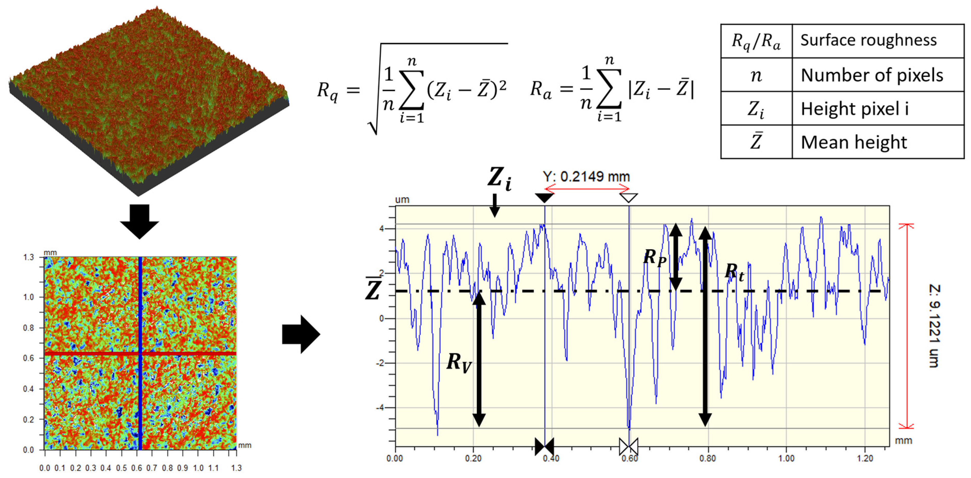
Appendix A.2. Roughness-Measurements

Figure A2. Explanatory schematics for roughness measurements and calculations.
Coatings 14 00808 g0a2

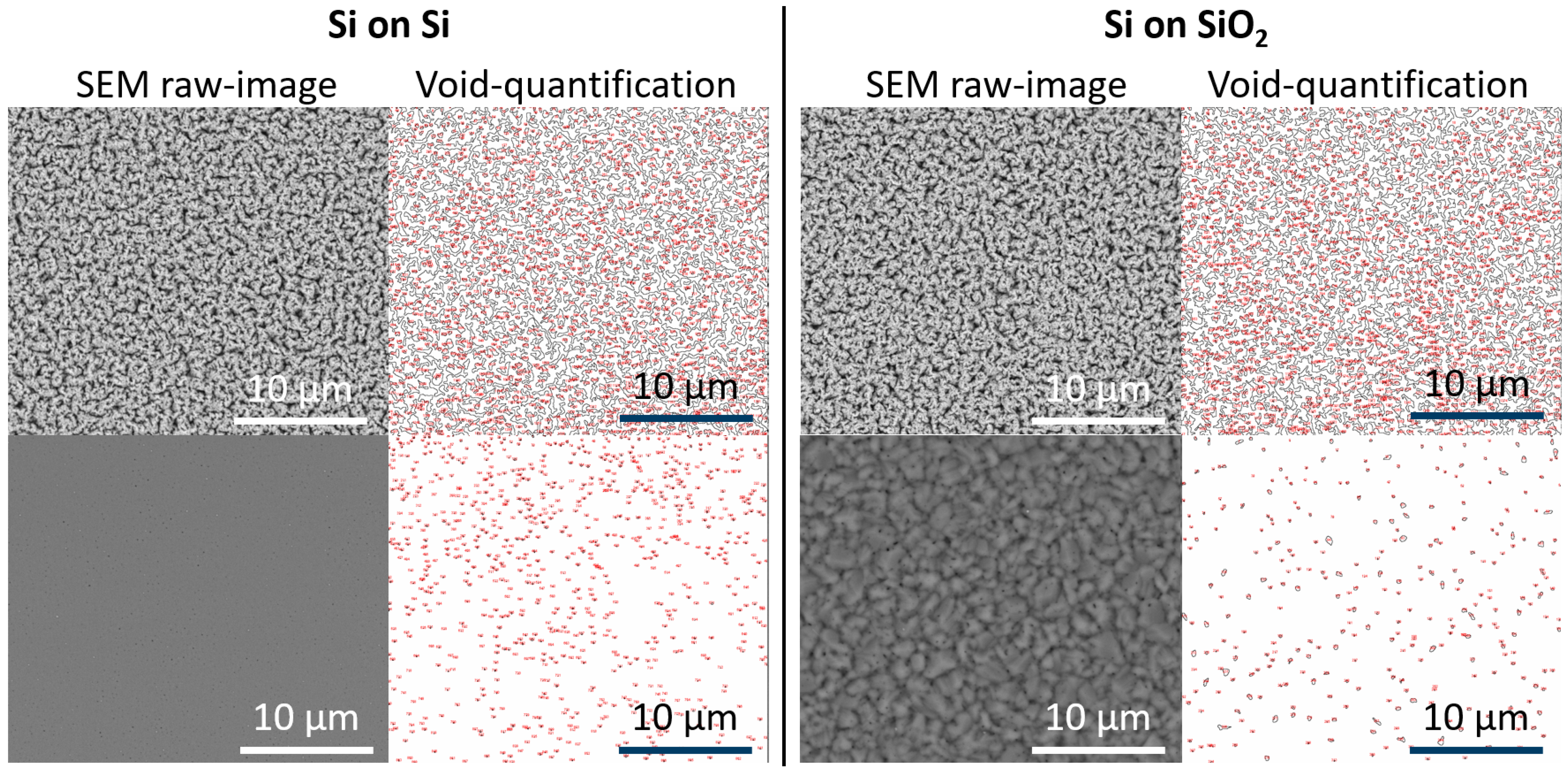
Appendix A.3. Void-Fraction Analysis

Figure A3. Examples of void-fraction analysis for Si-on-Si (left) and Si-on-SiO2 (right). 0.3 nm/s is exemplified in the top row, while 23.3 nm/s is exemplified in the bottom row. The reduction in size and number of voids in the SEM images for higher deposition rates is evident.
Coatings 14 00808 g0a3

Appendix A.4. Exponential Fits

The microstructural trends show good exponential fits f r d = A e B · r d . For the roughness this gives R q ( r d ) S i O 2 = 93 e 0.06 r d nm, R q ( r d ) S i = 38 e 0.69 r d nm with R S i O 2 2 = 0.76 and R S i 2 = 0.92 for S i O 2 and Si, respectively. We note the low correlation for the films on S i O 2 and the higher correlation on Si. Similarly, the void fraction follows V ( r d ) S i O 2 = 29 e 0.62 r d %, V ( r d ) S i = 31 e 0.61 r d % with R S i O 2 2 = 0.94 and R S i 2 = 0.95 for S i O 2 and Si.
The microstructural trends show exponential decays with the deposition rate: for the roughness, the correlation is high for Si-on-Si with a decaying trend: R q ( r d ) S i = 38 e 0.69 r d nm with R S i 2 = 0.92 . This is not the case for Si-on- S i O 2 , in which R d increases slightly with the deposition rate, yet with low fitting correlation. Similarly, the void fraction decays with the deposition rate, following V ( r d ) S i O 2 = 29 e 0.62 r d %, V ( r d ) S i = 31 e 0.61 r d % with R S i O 2 2 = 0.94 and R S i 2 = 0.95 for S i O 2 and Si.

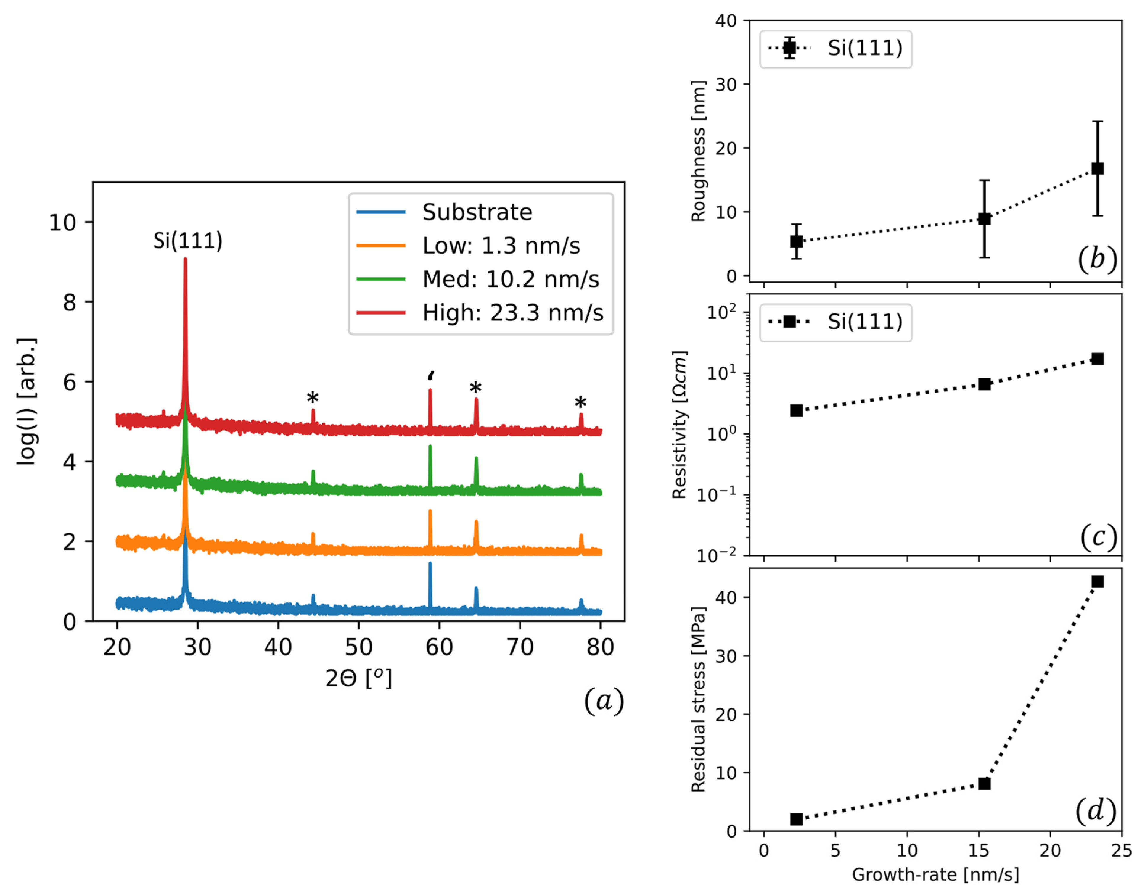
Appendix A.5. Depositions on (111)-Oriented Si

XRD patterns in Figure A4a confirm that silicon films grown on Si(111)-oriented wafers grow epitaxially in the 111 direction, as confirmed by the Si(111) reflection at 2q = 28.443° and the absence of reflections from other crystallographic orientations. In addition to the Si(111) reflection, the forbidden reflection Si(222) is present at approximately 2q = 58.9°. However, the roughness, resistivity, and residual stress increase with the deposition rate on Si(111), as shown in Figure A4b–d.
Figure A4. (a): XRD-patterns for Si deposited on Si(111): only the Si(111)-peak appearing shows that the films are epitaxial (* and ‘ are forbidden and stage-reflections). (bd) show roughness, resistivity, and residual stress as a function of deposition rate.
Coatings 14 00808 g0a4

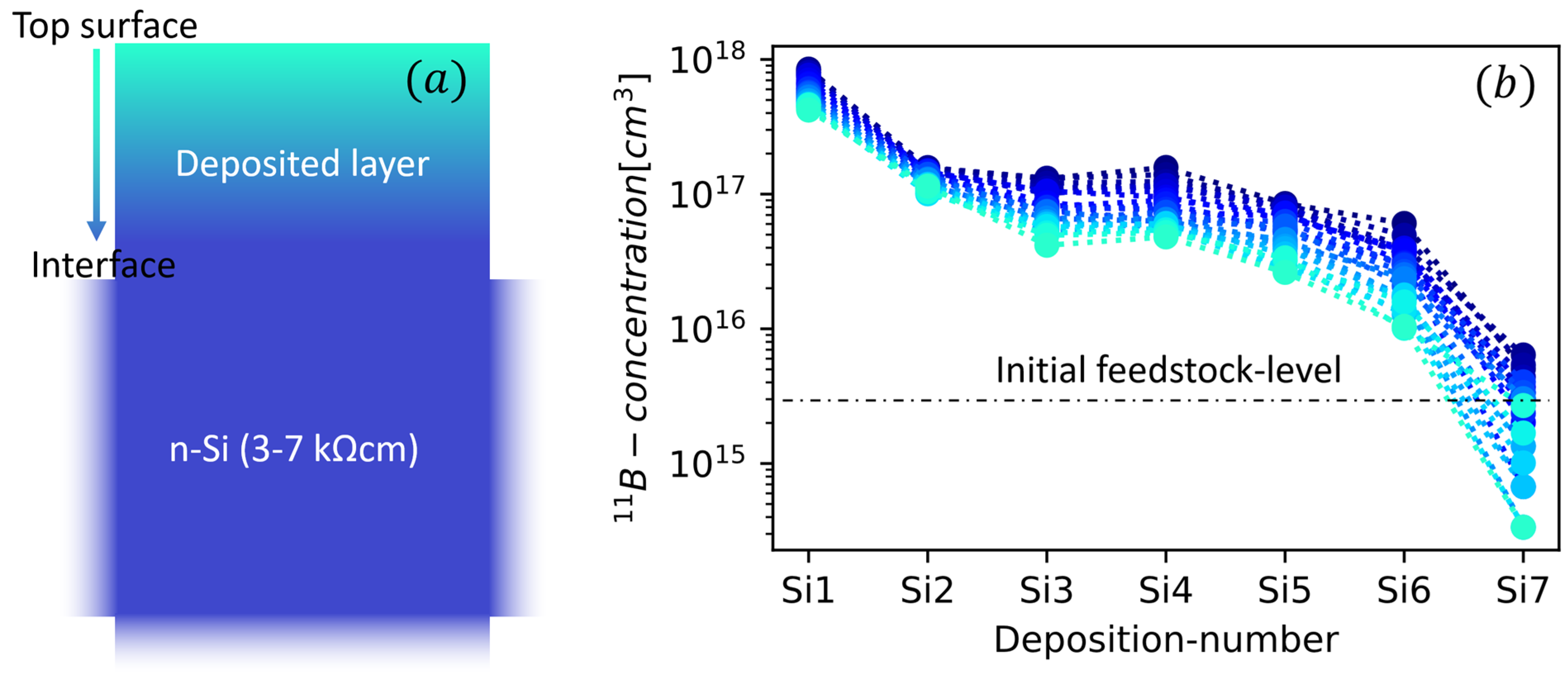
Appendix A.6. Boron Concentration in the Thin Films

Figure A5. SIMS measurements of the B-concentration in Si1–Si7 compared with the feedstock level. A schematic representation of the deposited film on the substrate is shown in (a), and measurements in (b). A lighter color indicates the top of the surface (material arriving latest), and darker colors represent the interface to the Si substrate (material being deposited earlier). The spread increases, and the transferred dopant concentration decreases as the melt is depleted for each consecutive deposition. B-atoms are transferred to the film from the melt to a larger extent than the Si-atoms; thus, the concentration is always significantly higher than that of the feedstock. After the melt is depleted, the B-dopants must also be rejuvenated. The challenge can be solved using effusion cells in the vacuum chamber, adding the dopants lost in the target substrate transfer.
Coatings 14 00808 g0a5

References

  1. Yoshikawa, K.; Kawasaki, H.; Yoshida, W.; Irie, T.; Konishi, K.; Nakano, K.; Uto, T.; Adachi, D.; Kanematsu, M.; Uzu, H.; et al. Silicon heterojunction solar cell with interdigitated back contacts for a photoconversion efficiency over 26%. Nat. Energy 2017, 2, 17032. [Google Scholar] [CrossRef]
  2. Sun, L.; Liu, Y.; Shao, R.; Wu, J.; Jiang, R.; Jin, Z. Recent progress and future perspective on practical silicon anode-based lithium ion batteries. Energy Storage Mater. 2022, 46, 482–502. [Google Scholar] [CrossRef]
  3. Zhao, H.; Li, J.; Zhao, Q.; Huang, X.; Jia, S.; Ma, J.; Ren, Y. Si-Based Anodes: Advances and Challenges in Li-Ion Batteries for Enhanced Stability. Electrochem. Energy Rev. 2024, 7, 11. [Google Scholar] [CrossRef]
  4. Saager, S.; Scheffel, B.; Zywitzki, O.; Modes, T.; Piwko, M.; Doerfler, S.; Althues, H.; Metzner, C. Porous silicon thin films as anodes for lithium ion batteries deposited by co-evaporation of silicon and zinc. Surf. Coat. Technol. 2019, 358, 586–593. [Google Scholar] [CrossRef]
  5. Margalit, N.; Xiang, C.; Bowers, S.M.; Bjorlin, A.; Blum, R.; Bowers, J.E. Perspective on the future of silicon photonics and electronics. Appl. Phys. Lett. 2021, 118, 220501. [Google Scholar] [CrossRef]
  6. Betta, G.F.D.; Povoli, M. Progress in 3D Silicon Radiation Detectors. Front. Phys. 2022, 10, 927690. [Google Scholar] [CrossRef]
  7. Tran, L.T.; Bolst, D.; James, B.; Pan, V.; Vohradsky, J.; Peracchi, S.; Chartier, L.; Debrot, E.; Guatelli, S.; Petasecca, M.; et al. Silicon 3d microdosimeters for advanced quality assurance in particle therapy. Appl. Sci. 2022, 12, 328. [Google Scholar] [CrossRef]
  8. Kok, A.; Povoli, M.; Summanwar, A.; Tran, L.T.; Petasecca, M.; Lerch, M.L.F.; Bolst, D.; Guatelli, S.; Rosenfeld, A.B. Fabrication and First Characterization of Silicon-Based Full 3-D Microdosimeters. IEEE Trans. Nucl. Sci. 2020, 67, 2490–2500. [Google Scholar] [CrossRef]
  9. Michael, A.; Kwok, C.Y.; Wang, P.; Kazuo, O.; Varlamov, S. Investigation of E-Beam Evaporated Silicon Film Properties for MEMS Applications. J. Microelectromechanical Syst. 2015, 24, 1951–1959. [Google Scholar] [CrossRef]
  10. Onaka-Masada, A.; Kadono, T.; Okuyama, R.; Hirose, R.; Kobayashi, K.; Suzuki, A.; Koga, Y.; Kurita, K. Reduction of dark current in cmos image sensor pixels using hydrocarbon-molecular-ion-implanted double epitaxial si wafers. Sensors 2020, 20, 1–18. [Google Scholar] [CrossRef]
  11. Grieco, C.; García, L.C.; Moreno, A.D.; Gkougkousis, E.; Grinstein, S.; Hidalgo, S.; Moffat, N.; Pellegrini, G.; Dominguez, J.V. Overview of CNM LGAD results: Boron Si-on-Si and epitaxial wafers. J. Instrum. 2022, 17, C09021. [Google Scholar] [CrossRef]
  12. Chen, P.H.; Chen, W.S.; Lee, C.H.; Wu, J.Y. Comprehensive Review of Crystalline Silicon Solar Panel Recycling: From Historical Context to Advanced Techniques. Sustainability 2024, 16, 60. [Google Scholar] [CrossRef]
  13. Weckend, S.; Wade, A.; Heath, G. End-of-Life Management: Solar Photovoltaic Panels: IEA PVPS Task 12: PV Sustainability. 2016. Available online: https://iea-pvps.org/wp-content/uploads/2020/01/IRENA_IEAPVPS_End-of-Life_Solar_PV_Panels_2016.pdf (accessed on 30 May 2024).
  14. Gielen, D.; Boshell, F.; Saygin, D.; Bazilian, M.D.; Wagner, N.; Gorini, R. The role of renewable energy in the global energy transformation. Energy Strategy Rev. 2019, 24, 38–50. [Google Scholar] [CrossRef]
  15. Stange, M.; Sunde, T.O.; Dahl-Hansen, R.; Rajput, K.; Graff, J.S.; Belle, B.D.; Ulyashin, A.G. High-Rate Epitaxial Growth of Silicon Using Electron Beam Evaporation at High Temperatures. Coatings 2023, 13, 2030. [Google Scholar] [CrossRef]
  16. Stange, M.S.S.; Sunde, T.O.; Dahl-Hansen, R.; Azar, A.S.; Graff, J.S.; Nørgaard, J.; Ulyashin, A.G. Epitaxial Growth of Silicon By Electron Beam Evaporation Deposition. In Proceedings of the 35th European Photovoltaic Solar Energy Conference and Exhibition, Brussels, Belgium, 24–28 September 2018; Volume 35. [Google Scholar]
  17. Solanki, C.S.; Carnel, L.; Van Nieuwenhuysen, K.; Ulyashin, A.; Posthuma, N.; Beaucarne, G.; Poortmans, J. Short Communication. Thin-film free-standing monocrystalline Si solar cells with heterojunction emitter. Prog. Photovolt. Res. Appl. 2005, 13, 201–208. [Google Scholar] [CrossRef]
  18. Dross, F.; Robbelein, J.; Vandevelde, B.; Van Kerschaver, E.; Gordon, I.; Beaucarne, G.; Poortmans, J. Stress-induced large-area lift-off of crystalline Si films. Appl. Phys. A Mater. Sci. Process 2007, 89, 149–152. [Google Scholar] [CrossRef]
  19. Janssen, G.C.A.M.; Abdalla, M.M.; van Keulen, F.; Pujada, B.R.; van Venrooy, B. Celebrating the 100th anniversary of the Stoney equation for film stress: Developments from polycrystalline steel strips to single crystal silicon wafers. Thin Solid Films 2009, 517, 1858–1867. [Google Scholar] [CrossRef]
  20. Caber, P.J. Interferometric profiler for rough surfaces. Appl. Opt. 1993, 32, 3438–3441. [Google Scholar] [CrossRef] [PubMed]
  21. Schindler, F.; Schubert, M.C.; Kimmerle, A.; Broisch, J.; Rein, S.; Kwapil, W.; Warta, W. Modeling majority carrier mobility in compensated crystalline silicon for solar cells. Sol. Energy Mater. Sol. Cells 2012, 106, 31–36. [Google Scholar] [CrossRef]
  22. Sugiura, H.; Yamaguchi, M. Crystal Defects of Silicon Films Formed by Molecular Beam Epitaxy. Jpn. J. Appl. Phys. 1980, 19, 583–589. [Google Scholar] [CrossRef]
  23. Shiraki, Y. Silicon Molecular Beam Epitaxy. Prog. Cryst. Growth Charact. 1986, 12, 45–66. [Google Scholar] [CrossRef]
  24. Abadias, G.; Chason, E.; Keckes, J.; Sebastiani, M.; Thompson, G.B.; Barthel, E.; Doll, G.L.; Murray, C.E.; Stoessel, C.H.; Martinu, L. Review Article: Stress in thin films and coatings: Current status, challenges, and prospects. J. Vac. Sci. Technol. A Vac. Surf. Film. 2018, 36, 020801. [Google Scholar] [CrossRef]
  25. Saedi, A.; Rost, M.J. Thermodynamics of deposition flux-dependent intrinsic film stress. Nat. Commun. 2016, 7, 10733. [Google Scholar] [CrossRef] [PubMed]
  26. Krause, B.; Abadias, G.; Michel, A.; Wochner, P.; Ibrahimkutty, S.; Baumbach, T. Direct Observation of the Thickness-Induced Crystallization and Stress Build-Up during Sputter-Deposition of Nanoscale Silicide Films. ACS Appl. Mater. Interfaces 2016, 8, 34888–34895. [Google Scholar] [CrossRef] [PubMed]
  27. Engwall, A.M.; Rao, Z.; Chason, E. Origins of residual stress in thin films: Interaction between microstructure and growth kinetics. Mater. Des. 2016, 110, 616–623. [Google Scholar] [CrossRef]
  28. Doerner, M.F.; Nix, W.D. Stresses and deformation processes in thin films on substrates. Crit. Rev. Solid State Mater. Sci. 1988, 14, 225–268. [Google Scholar] [CrossRef]
  29. Oberbeck, L.; Bergmann, R.B. Electronic properties of silicon epitaxial layers deposited by ion-assisted deposition at low temperatures. J. Appl. Phys. 2000, 88, 3015–3021. [Google Scholar] [CrossRef]
  30. Gorka, B.; Dogan, P.; Sieber, I.; Fenske, F.; Gall, S. Low-temperature epitaxy of silicon by electron beam evaporation. Thin Solid Films 2007, 515, 7643–7646. [Google Scholar] [CrossRef]
  31. Wagner, T.A.; Oberbeck, L.; Bergmann, R.B.; Werner, J.H. Intra-grain defects-limiting factor for low-temperature polycrystalline silicon films? In Solid State Phenomena; Trans Tech Publications Ltd.: Zurich, Switzerland, 2001; pp. 95–100. [Google Scholar] [CrossRef]
  32. Chason, E.; Shin, J.W.; Hearne, S.J.; Freund, L.B. Kinetic model for dependence of thin film stress on growth rate, temperature, and microstructure. J. Appl. Phys. 2012, 111, 083520. [Google Scholar] [CrossRef]
  33. Chason, E.; Sheldon, B.W.; Freund, L.B.; Floro, J.A.; Hearne, S.J. Origin of Compressive Residual Stress in Polycrystalline Thin Films. Phys. Rev. Lett. 2002, 88, 4. [Google Scholar] [CrossRef]
  34. Rabalais, J.W.; Al-Bayati, A.H.; Boyd, K.J.; Marton, D.; Kulik, J.; Zhang, Z.; Chu, W.K. Ion-energy effects in silicon ion-beam epitaxy. Phys. Rev. B 1996, 53, 10781–10792. [Google Scholar] [CrossRef] [PubMed]
  35. Brinciotti, E.; Gramse, G.; Hommel, S.; Schweinboeck, T.; Altes, A.; Fenner, M.A.; Smoliner, J.; Kasper, M.; Badino, G.; Tuca, S.-S.; et al. Probing resistivity and doping concentration of semiconductors at the nanoscale using scanning microwave microscopy. Nanoscale 2015, 7, 14715–14722. [Google Scholar] [CrossRef]
  36. Masetti, G.; Severi, M.; Solmi, S. Modeling of Carrier Mobility against Carrier Concentration in Arsenic-, Phosphorus-, and Boron-lhped Silicon. IEEE Trans. Electron Devices 1983, 30, 764–769. [Google Scholar] [CrossRef]
Figure 1. Schematic (a) and actual (b) experimental setup. The stainless-steel Si-recollector unit is filled with removable Si wafers along the inside to recollect stray material flux. The rate is monitored by a shuttered crystal-quartz monitor (QCM). A refilled and stabilized melt with a volume of 500 cm3 is shown in (c,d).
Coatings 14 00808 g001
Figure 2. θ − 2θ XRD patterns of silicon films grown on Si (a) and oxidized S i O 2 (b). Reflections marked (*) originate from the sample stage, while reflections marked with (‘) are forbidden Si reflections.
Coatings 14 00808 g002
Figure 3. SEM images of films deposited on Si (upper row) and S i O 2 (lower) for low to high deposition rates. While films with a coarse microstructure were obtained at r d < 1 nm/s, crystalline films grew for all higher rates investigated here. At r d > 1 nm/s, the films grown on Si had significantly fewer defects than on S i O 2 . In both instances, the increasing r d resulted in larger coalesced grains.
Coatings 14 00808 g003
Figure 4. Comparison of Si-on- S i O 2 and Si-on-Si substrates in the upper and lower row. (a) shows pictograms of a substrate with film at low and high deposition rates. (b) shows examples of curvature measurements before (left) and after (right) film deposition.
Coatings 14 00808 g004
Figure 5. Measured key film properties as a function of deposition rate, r d , for Si-on-Si (blue) and S i O 2 (orange): surface roughness, R q , from WLI-data in (a) void fraction, V f ; from SEM-image analysis (b); and resistivity, ρ f i l m , from four-point probing (c). The measured residual film stresses, σ , as a function of deposition rate (d): positive values (upward curvature) indicate tensile stress, and negative values (downward curvature) compressive stress. The inset graphs show the curvature of the wafers of Si3, highlighted with a red circle: solid blue lines indicate the measured curve and the dashed magenta-lines the fit to the curve, using R 2 > 0.95 as general fitting criteria.
Coatings 14 00808 g005
Table 1. Measured values for all film substrate systems. The leftmost column indicates the experimental order.
Run #Rate [nm/s]Roughness [nm]Void Fraction [%] Resistivity   [ Ω · c m ]Residual Stress [MPa]
SiSiO2SiSiO2SiSiO2SiSiO2
Si1 0.3 ± 0.2 41 ± 5 79 ± 6 32.931.10.030.72−41.96.0
Si2 1.1 ± 0.8 15 ± 4 111 ± 8 12.712.00.141.17−31.68.9
Si3 1.6 ± 1.2 8 ± 1 114 ± 8 8.27.60.161.38−29.140.2
Si4 2.3 ± 1.5 8 ± 2 108 ± 7 7.16.50.313.70−18.330.2
Si5 7 ± 1 6 ± 3 125 ± 8 6.53.70.416.06−17.531.1
Si6 10 ± 5 5 ± 1 115 ± 6 3.53.40.6310.89−16.938.0
Si7 10 ± 6 4 ± 2 119 ± 7 0.93.00.7111.90−12.330.0
Si8 11 ± 5 4 ± 2 120 ± 10 0.92.90.7411.77−10.033.3
Si9 15 ± 2 3 ± 1 156 ± 9 0.62.40.9229.66−7.035.2
Si10 23 ± 3 2.7 ± 1.1 159 ± 9 0.21.52.0868.37−6.738.6
Disclaimer/Publisher’s Note: The statements, opinions and data contained in all publications are solely those of the individual author(s) and contributor(s) and not of MDPI and/or the editor(s). MDPI and/or the editor(s) disclaim responsibility for any injury to people or property resulting from any ideas, methods, instructions or products referred to in the content.

