
Sol-Gel Derived ZnO Thin Films with Nonvolatile Resistive Switching Behavior for Future Memory Applications


Abstract
:1. Introduction
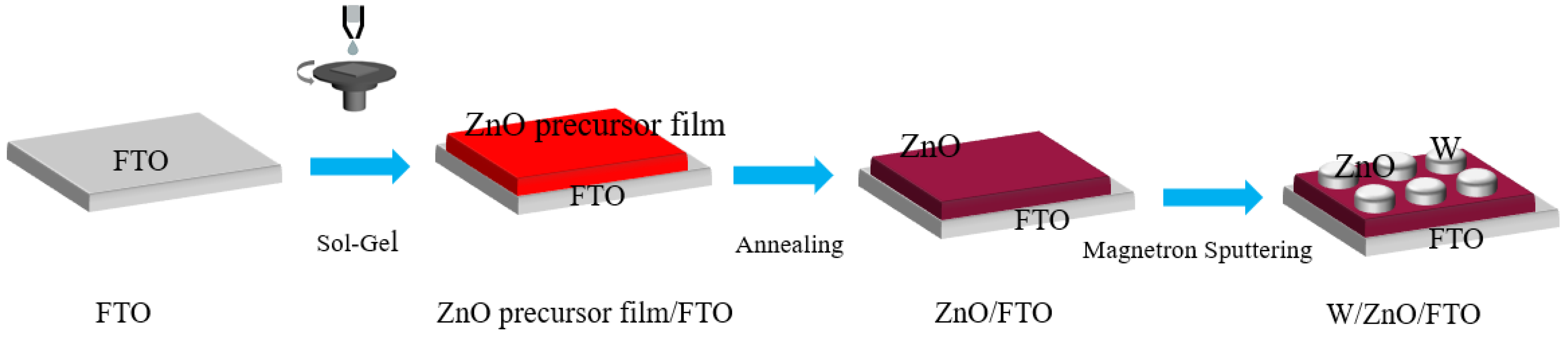
2. Experimental
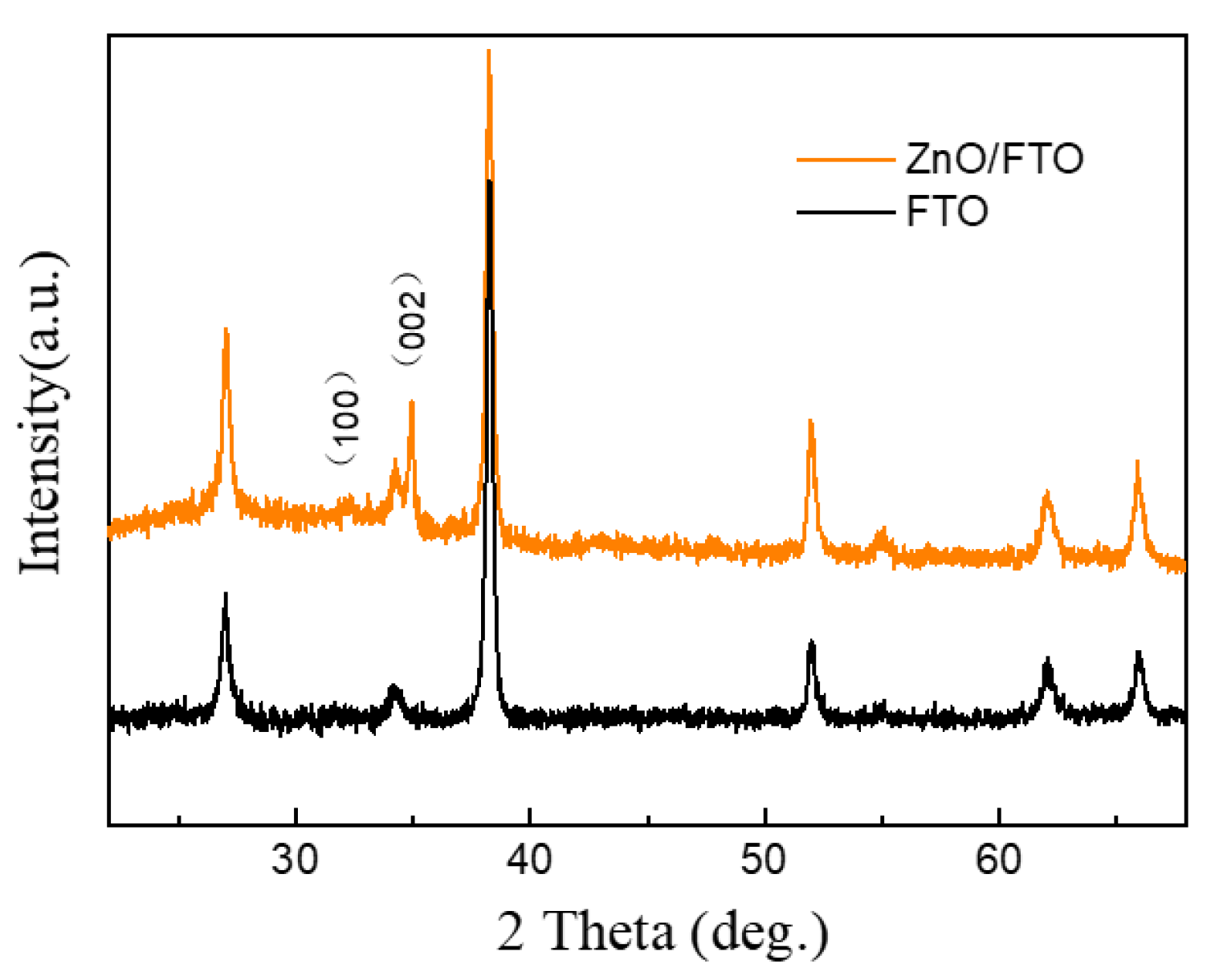
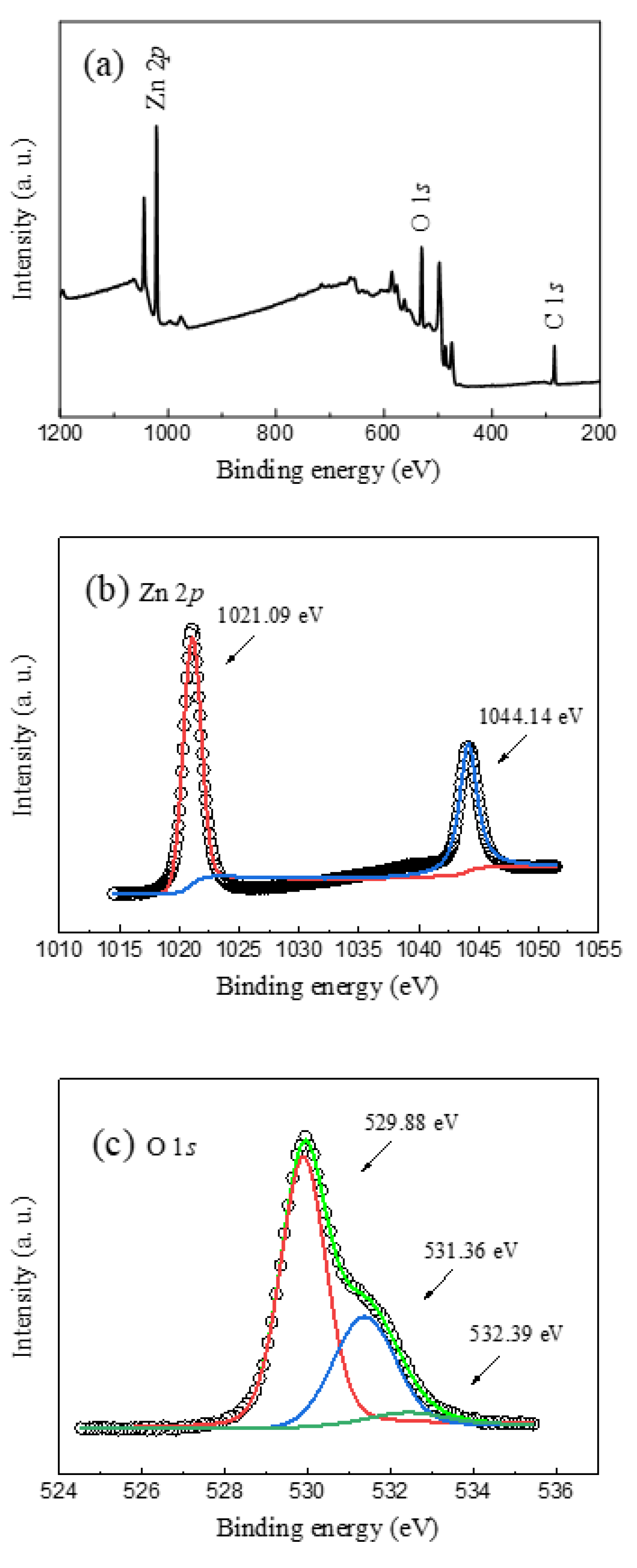
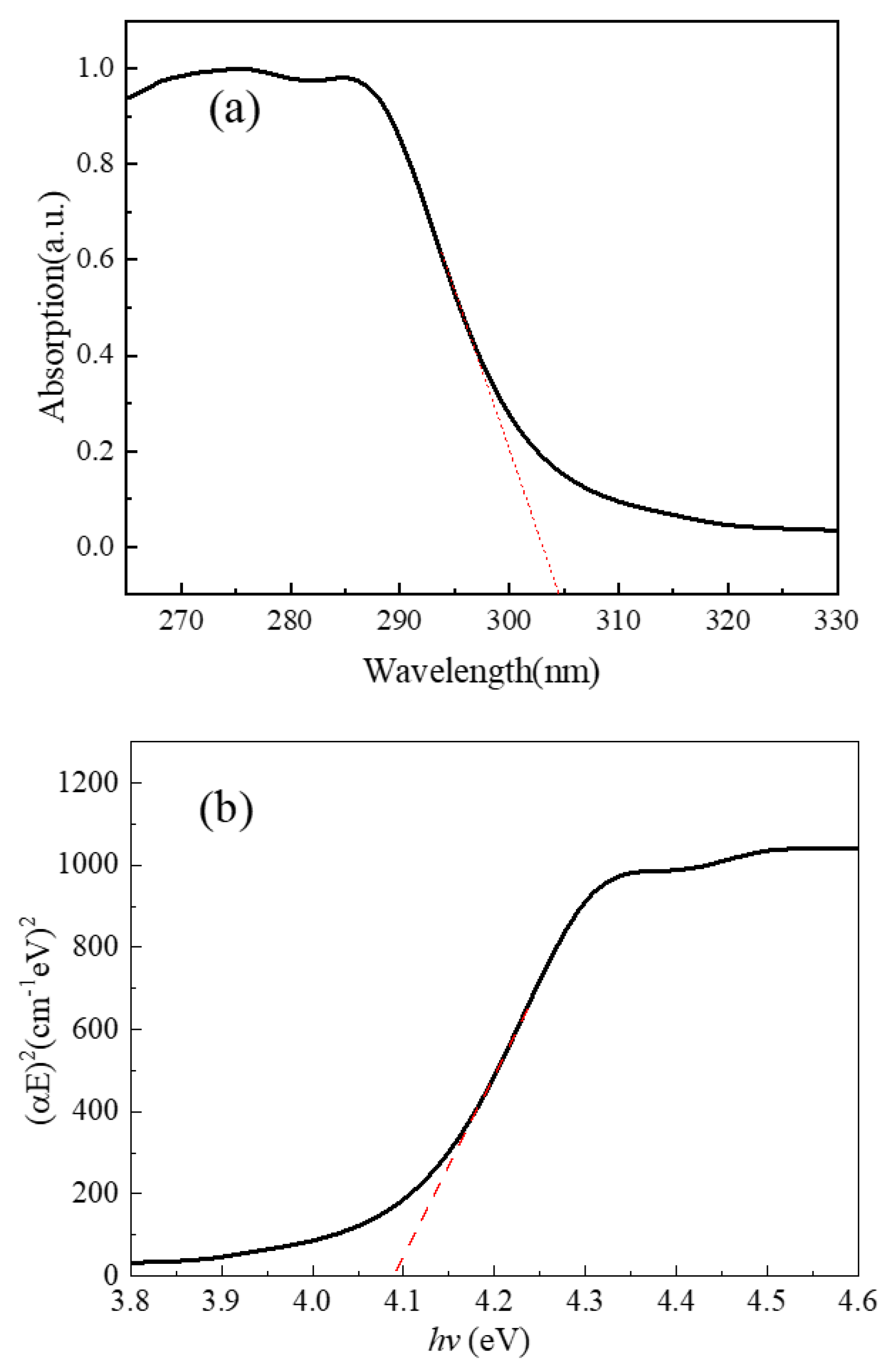
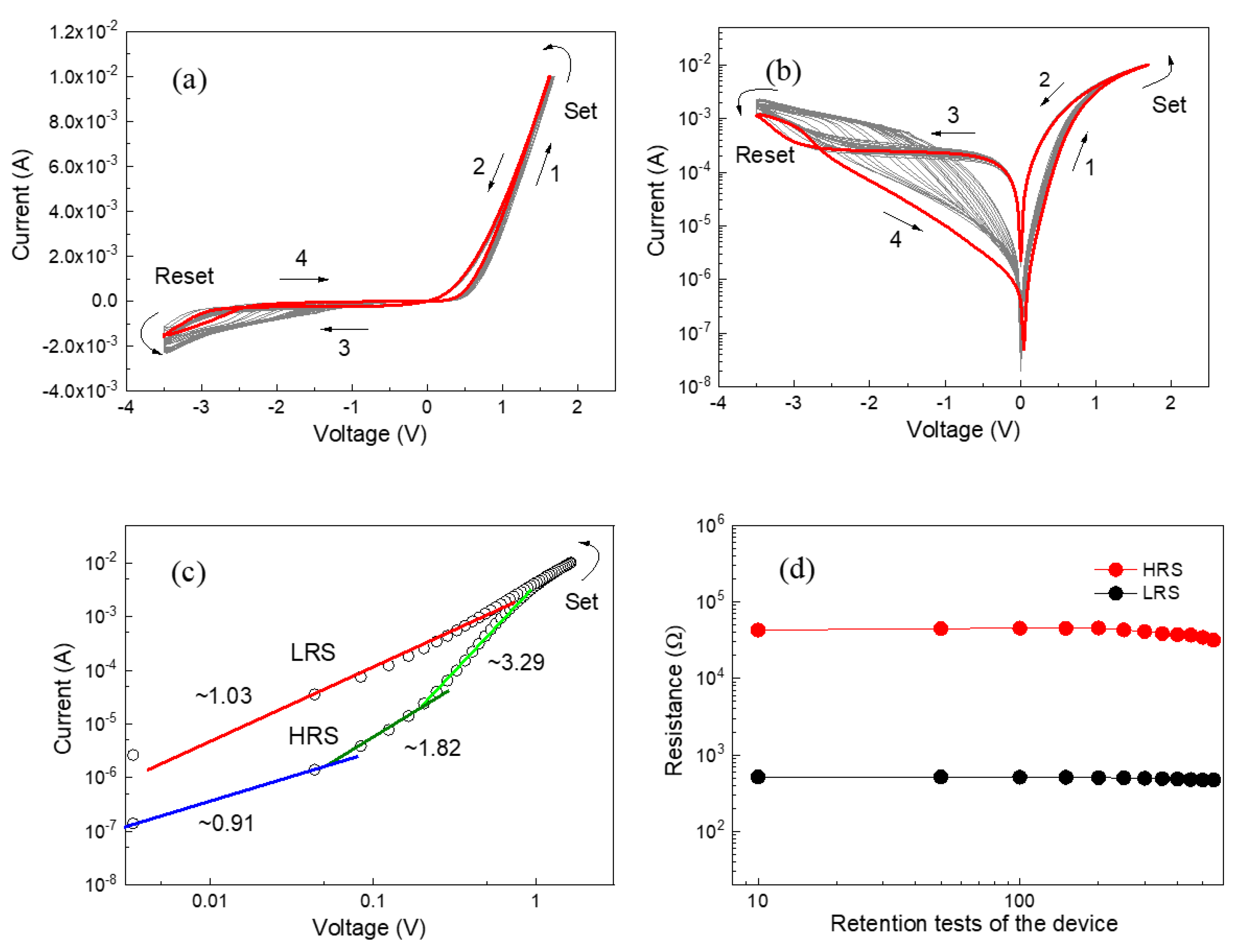
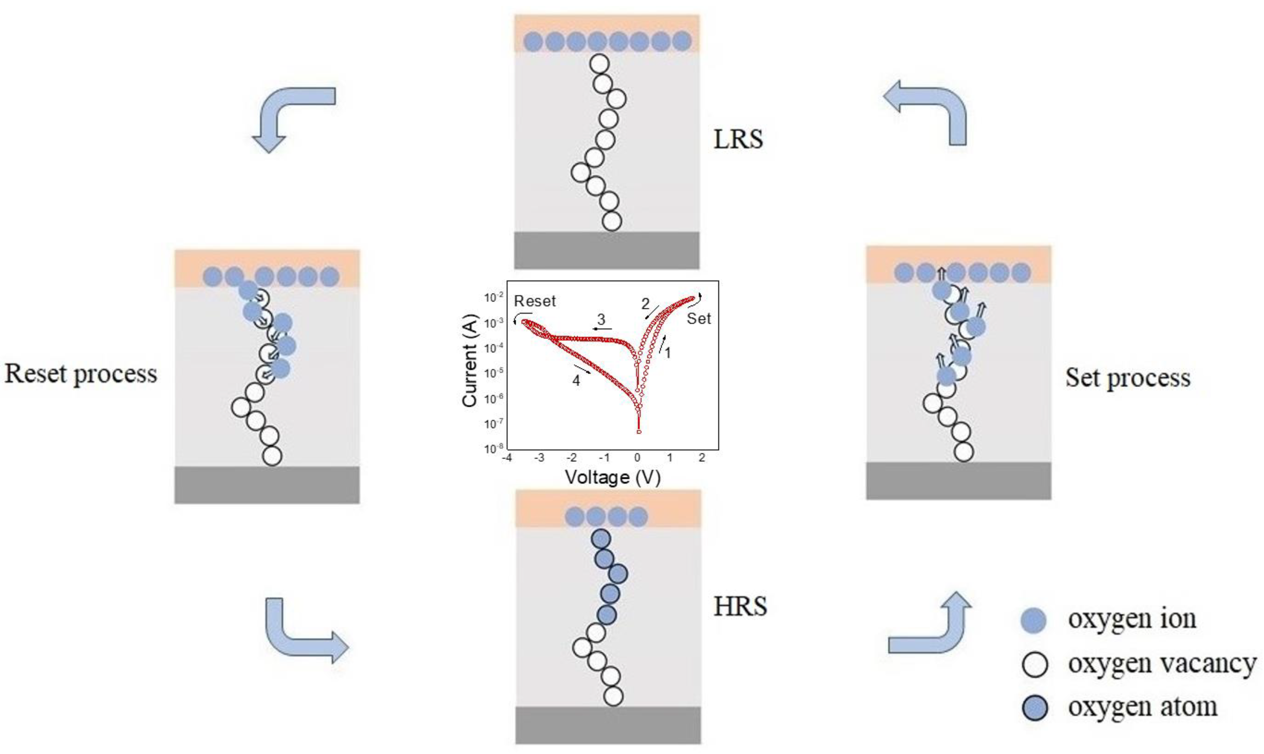
3. Results and Discussion
4. Conclusions
Author Contributions
Funding
Institutional Review Board Statement
Informed Consent Statement
Data Availability Statement
Conflicts of Interest
References
- Chua, L.O. Memristor-The missing circuit element. IEEE Trans. Circuit Theory 1971, 18, 507–519. [Google Scholar] [CrossRef]
- Strukov, D.B.; Snider, G.S.; Stewart, D.R.; Williams, R.S. The missing memristor found. Nature 2008, 453, 80–83. [Google Scholar] [CrossRef]
- Milano, G.; Luebben, M.; Ma, Z.; Dunin-Borkowski, R.; Boarino, L.; Pirri, C.F.; Waser, R.; Ricciardi, C.; Valov, I. Self-limited single nanowire systems combining allin-one memristive and neuromorphic functionalities. Nat. Commun. 2018, 9, 5151. [Google Scholar] [CrossRef] [PubMed]
- Ren, S.X.; Dong, W.C.; Tang, H.; Tang, L.Z.; Li, Z.H.; Sun, Q.; Yang, H.F.; Yang, Z.G.; Zhao, J.J. High-efficiency magnetic modulation in Ti/ZnO/Pt resistive random-access memory devices using amorphous zinc oxide film. Appl. Surf. Sci. 2019, 488, 92–97. [Google Scholar] [CrossRef]
- Sarkar, D.; Singh, A.K. Mechanism of Nonvolatile Resistive Switching in ZnO/α-Fe2O3 Core-Shell Heterojunction Nanorod Arrays. J. Phys. Chem. C 2017, 121, 12953–12958. [Google Scholar] [CrossRef]
- Yu, Z.Q.; Jia, J.H.; Qu, X.R.; Wang, Q.C.; Kang, W.B.; Liu, B.S.; Xiao, Q.Q.; Gao, T.H.; Xie, Q. Tunable resistive switching behaviors and mechanism of the W/ZnO/ITO memory cell. Molecules 2023, 28, 5313. [Google Scholar] [CrossRef]
- Qi, M.; Zhang, X.; Yang, L.; Wang, Z.Q.; Xu, H.Y.; Liu, W.Z.; Zhao, X.N.; Liu, Y.C. Intensity-modulated LED achieved through integrating p-GaN/n-ZnO heterojunction with multilevel RRAM. Appl. Phys. Lett. 2018, 113, 223503. [Google Scholar] [CrossRef]
- Chen, J.; Wu, Y.L.; Zhu, K.L.; Sun, F.; Guo, C.G.; Wu, X.L.; Cheng, G.A.; Zheng, R.T. Core-shell copper nanowire-TiO2 nanotube arrays with excellent bipolar resistive switching properties. Electrochim. Acta 2019, 316, 133–142. [Google Scholar] [CrossRef]
- Kyung, M.K.; Byung, J.C.; Yong, C.S.; Seol, C.; Cheol, S.H. Anode-interface localized filamentary mechanism in resistive switching of TiO2 thin film. Appl. Phys. Lett. 2007, 91, 012907. [Google Scholar] [CrossRef]
- Yu, Z.Q.; Sun, T.Y.; Liu, B.S.; Zhang, L.; Chen, H.J.; Fan, X.S.; Sun, Z.J. Self-rectifying and forming-free nonvolatile memory behavior in single-crystal TiO2 nanowire memory device. J. Alloys Compd. 2021, 858, 157749. [Google Scholar] [CrossRef]
- Persson, K.M.; Ram, M.S.; Kilpi, O.P.; Borg, M.; Wernersson, L.E. Cross-Point Arrays with Low-Power ITO-HfO2 Resistive Memory Cells Integrated on Vertical III-V Nanowires. Adv. Electron. Mater. 2020, 6, 2000154. [Google Scholar] [CrossRef]
- Mahmoud, N.A.; Maximilian, S.; Brian, C.O.; Erik, J.L.; Sayed, Y.S.; Marc, T.; Jillian, M.B. Bipolar Resistive Switching in Junctions of Gallium Oxide and p-type Silicon. Nano Lett. 2021, 21, 2666–2674. [Google Scholar] [CrossRef]
- Yu, Z.Q.; Xu, J.M.; Liu, B.S.; Sun, Z.J.; Huang, Q.N.; Ou, M.L.; Wang, Q.C.; Jia, J.H.; Kang, W.B.; Xiao, Q.Q.; et al. A Facile Hydrothermal Synthesis and Resistive Switching Behavior of α-Fe2O3 Nanowire Arrays. Molecules 2023, 28, 3835. [Google Scholar] [CrossRef] [PubMed]
- Yao, C.Y.; Li, J.C.; Thatikonda, S.K.; Ke, Y.F.; Qin, N.; Bao, D.H. Introducing a thin MnO2 layer in Co3O4-based memory to enhance resistive switching and magnetization modulation behaviors. J. Alloys Compd. 2020, 823, 153731. [Google Scholar] [CrossRef]
- Huang, C.H.; Matsuzaki, K.; Nomura, K. Threshold switching of non-stoichiometric CuO nanowire for selector application. Appl. Phys. Lett. 2020, 116, 023503. [Google Scholar] [CrossRef]
- Hsu, C.C.; Wang, S.Y.; Lin, Y.S.; Chen, Y.T. Self-rectifying and interface-controlled resistive switching characteristics of molybdenum oxide. J. Alloys Compd. 2019, 779, 609–617. [Google Scholar] [CrossRef]
- You, B.K.; Park, W.I.; Kim, J.M.; Park, K.I.; Seo, H.K.; Lee, J.Y.; Jung, Y.S.; Lee, K.J. Formation in Resistive Memories by Self-Assembled Nanoinsulators Derived from a Block Copolymer. ACS NANO 2014, 9, 9492–9502. [Google Scholar] [CrossRef] [PubMed]
- Huang, C.H.; Chang, W.C.; Huang, J.S.; Lin, S.M.; Chueh, Y.L. Resistive Switching of Sn-doped In2O3/HfO2 core-shell nanowire: Geometry Architecture Engineering for Nonvolatile Memory. Nanoscale 2017, 9, 6920–6928. [Google Scholar] [CrossRef] [PubMed]
- Sun, Y.M.; Song, C.; Yin, J.; Qiao, L.L.; Wang, R.; Wang, Z.Y.; Chen, X.Z.; Yin, S.Q.; Saleem, M.S.; Wu, H.Q.; et al. Modulating metallic conductive filaments via bilayer oxides in resistive switching memory. Appl. Phys. Lett. 2019, 114, 193502. [Google Scholar] [CrossRef]
- Younis, A.; Chu, D.W.; Li, S.A. Stochastic memristive nature in Co-doped CeO2 nanorod arrays. Appl. Phys. Lett. 2013, 103, 253504. [Google Scholar] [CrossRef]
- Zoolfakar, A.S.; Kadir, R.A.; Rani, R.A.; Balendhran, S.; Liu, X.J.; Kats, E.; Bhargava, S.K.; Bhaskaran, M.; Sriram, S.; Zhuiykov, S.; et al. A comprehensive review of ZnO materials and devices. Phys. Chem. Chem. Phys. 2013, 15, 10376. [Google Scholar] [CrossRef]
- Park, J.; Biju, K.P.; Jung, S.; Lee, W.; Lee, J.; Kim, S.; Park, S.; Shin, J.; Hwang, H. Multibit Operation of TiOx-Based ReRAM by Schottky Barrier Height Engineering. IEEE Electron Device Lett. 2011, 32, 476–478. [Google Scholar] [CrossRef]
- Liang, K.; Huang, C.; Lai, C.; Huang, J.; Tsai, H.; Wang, Y.; Shih, Y.; Chang, M.; Lo, S.; Chueh, Y. Single CuOx Nanowire Memristor: Forming-Free Resistive Switching Behavior. ACS Appl. Mater. Interfaces 2014, 6, 16537–16544. [Google Scholar] [CrossRef]
- Wang, F.J.; Chen, K.J.; Yi, X.R.; Lin, Y.N.; Zhuang, S.L. A study on sodium alginate based memristor: From typical to self-rectifying. Mater. Lett. 2023, 338, 134037. [Google Scholar] [CrossRef]
- Miccoli, I.; Spampinato, R.; Marzo, F.; Prete, P.; Lovergine, N. DC-magnetron sputtering of ZnO:Al films on (00.1)Al2O3 substrates from slip-casting sintered ceramic targets. Appl. Surf. Sci. 2014, 313, 418–423. [Google Scholar] [CrossRef]
- Lehraki, N.; Aida, M.S.; Abed, S.; Attaf, N.; Attaf, A.; Poulain, M. ZnO thin films deposition by spray pyrolysis: Influence of precursor solution properties. Curr. Appl. Phys. 2012, 12, 1283–1287. [Google Scholar] [CrossRef]
- Milano, G.; Porro, S.; Ali, M.Y.; Bejtka, K.; Bianco, S.; Beccaria, F.; Chiolerio, A.; Pirri, C.F.; Ricciardi, C. Unravelling Resistive Switching Mechanism in ZnO NW Arrays: The Role of the Polycrystalline Base Layer. J. Phys. Chem. C 2018, 12, 866–874. [Google Scholar] [CrossRef]
- Garratt, E.; Prete, P.; Lovergine, N.; Nikoobakht, B. Observation and Impact of a “Surface Skin Effect” on Lateral Growth of Nanocrystals. J. Phys. Chem. C 2017, 121, 14845–14853. [Google Scholar] [CrossRef]
- Zhang, J.; Yang, H.; Zhang, Q.L.; Dong, S.R.; Luo, J.K. Bipolar resistive switching characteristics of low temperature grown ZnO thin films by plasma-enhanced atomic layer deposition. Appl. Phys. Lett. 2013, 102, 012113. [Google Scholar] [CrossRef]
- Khan, S.A.; Rahmani, M.K.; Khan, W.U.; Kim, J.; Bae, J.; Kang, M.H. Multistate Resistive Switching with Self-Rectifying Behavior and Synaptic Characteristics in a Solution-processed ZnO/PTAA Bilayer Memristor. J. Electrochem. Soc. 2022, 169, 063517. [Google Scholar] [CrossRef]
- Sokolov, A.S.; Jeon, Y.R.; Kim, S.; Ku, B.; Choi, C. Bio-realistic synaptic characteristics in the cone-shaped ZnO memristive device. NPG Asia Mater. 2019, 11, 5. [Google Scholar] [CrossRef]
- Quintana, A.; Gómez, A.; Baró, M.D.; Suriñach, S.; Pellicer, E.; Sort, J. Self-templating faceted and spongy single-crystal ZnO nanorods: Resistive switching and enhanced piezoresponse. Mater. Des. 2017, 133, 54–61. [Google Scholar] [CrossRef]
- Reddy, I.N.; Reddy, C.V.; Sreedhar, M.; Cho, M.; Shim, J.; Reddy, V.R.; Choi, C.-J.; Kim, D. Effect of seed layers (Al, Ti) on optical and morphology of Fe-doped ZnO thin film nanowires grown on Si substrate via electron beam evaporation. Mater. Sci. Semicond. Process. 2017, 71, 296–303. [Google Scholar] [CrossRef]
- Sekhar, K.C.; Kamakshi, K.; Bernstorff, S.; Gomes, M.J.M. Effect of annealing temperature on photoluminescence and resistive switching characteristics of ZnO/Al2O3 multilayer nanostructures. J. Alloys Compd. 2015, 619, 248–252. [Google Scholar] [CrossRef]
- Zhou, Z.; Xiu, F.; Jiang, T.F.; Xu, J.G.; Chen, J.; Liu, J.Q.; Huang, W. Solution-processable zinc oxide nanorods and a reduced graphene oxide hybrid nanostructure for highly flexible and stable memristor. J. Mater. Chem. C 2019, 7, 10764–10768. [Google Scholar] [CrossRef]
- Punugupati, S.; Temizer, N.K.; Narayan, J.; Hunte, F. Structural and resistance switching properties of epitaxial Pt/ZnO/TiN/Si(001) heterostructures. J. Appl. Phys. 2014, 115, 234501. [Google Scholar] [CrossRef]
- Manna, A.K.; Dash, P.; Das, D.; Srivastava, S.K.; Sahoo, P.K.; Kanjilal, A.; Kanjilal, D.; Varma, S. Resistive switching properties and photoabsorption behavior of Ti ion implanted ZnO thin films. Ceram. Int. 2022, 48, 3303–3310. [Google Scholar] [CrossRef]
- Sun, Y.H.; Yan, X.Q.; Zheng XLiu, Y.H.; Zhao, Y.G.; Shen, Y.W.; Liao, Q.L.; Zhang, Y. High On-Off Ratio Improvement of ZnO-Based Forming-Free Memristor by Surface Hydrogen Annealing. ACS Appl. Mater. Interfaces 2015, 7, 7382–7388. [Google Scholar] [CrossRef]
- Xu, Z.D.; Yu, L.N.; Xu, X.G.; Miao, J.; Jiang, Y. Effect of oxide/oxide interface on polarity dependent resistive switching behavior in ZnO/ZrO2 heterostructures. Appl. Phys. Lett. 2014, 104, 192903. [Google Scholar] [CrossRef]
- Huang, J.S.; Lee, C.Y.; Chin, T.S. Forming-free bipolar memristive switching of ZnO films deposited by cyclic-voltammetry. Electrochim. Acta 2013, 91, 62–68. [Google Scholar] [CrossRef]
- Park, J.J.; Lee, S.H.; Lee, J.H.; Yong, K.J. A Light Incident Angle Switchable ZnO Nanorod Memristor: Reversible Switching Behavior Between Two Non-Volatile Memory Devices. Adv. Mater. 2013, 25, 6423–6429. [Google Scholar] [CrossRef]
- Shen, X.; Lin, X.; Peng, Y.; Zhang, Y.; Long, F.; Han, Q.; Wang, Y.; Han, L. Two-Dimensional Materials for Highly Efficient and Stable Perovskite Solar Cells. Nano-Micro Lett. 2024, 16, 201. [Google Scholar] [CrossRef]
- Wu, S.J.; Wang, F.; Zhang, Z.C.; Li, Y.; Han, Y.M.; Yang, Z.C.; Zhao, J.S.; Zhang, K.L. High uniformity and forming-free ZnO-based transparent RRAM with HfOx inserting layer. Chin. Phys. B 2018, 27, 087701. [Google Scholar] [CrossRef]
- Simanjuntak, F.M.; Ohno, T.; Samukawa, S.J. Neutral Oxygen Beam Treated ZnO-Based Resistive Switching Memory Device. ACS Appl. Electron. Mater. 2019, 1, 18–24. [Google Scholar] [CrossRef]
- Jung, J.; Kwon, D.; Jung, H.; Lee, K.; Yoon, T.; Kang, C.J.; Lee, H.H. Multistate resistive switching characteristics of ZnO nanoparticles embedded polyvinylphenol device. J. Ind. Eng. Chem. 2018, 64, 85–89. [Google Scholar] [CrossRef]
- Choi, K.H.; Mustafa, M.; Rahman, K.; Jeong, B.K.; Doh, Y.H. Cost-effective fabrication of memristive devices with ZnO thin film using printed electronics technologies. Appl. Phys. A 2012, 106, 165–170. [Google Scholar] [CrossRef]
- Patil, S.R.; Chougale, M.Y.; Rane, T.D.; Khot, S.S.; Patil, A.A.; Bagal, O.S.; Jadhav, S.D.; Sheikh, A.D.; Kim, S.; Dongale, T.D. Solution-Processable ZnO Thin Film Memristive Device for Resistive Random Access Memory Application. Electronics 2018, 7, 445. [Google Scholar] [CrossRef]
- Chang, W.Y.; Lin, C.; He, J.; Wu, T. Resistive switching behaviors of ZnO nanorod layers. Appl. Phys. Lett. 2012, 96, 242109. [Google Scholar] [CrossRef]
- Wang, J.R.; Pan, R.B.; Cao, H.T.; Wang, Y.; Liang, L.Y.; Zhang, H.L.; Gao, J.H.; Zhuge, F. Anomalous rectification in a purely electronic memristor. Appl. Phys. Lett. 2016, 109, 143505. [Google Scholar] [CrossRef]
- Karthik, K.R.G.; Prabhakar, R.R.; Hai-, L.; Batabyal, S.K.; Huang, Y.Z.; Mhaisalkar, S.G. A ZnO nanowire resistive switch. Appl. Phys. Lett. 2013, 103, 123114. [Google Scholar] [CrossRef]
- Sun, B.; Liu, Y.H.; Zhao, W.X.; Chen, P. Magnetic-field and white-light controlled resistive switching behaviors in Ag/BiFeO3/γ-Fe2O3/FTO device. RSC Adv. 2015, 5, 13513–13518. [Google Scholar] [CrossRef]
- Huang, C.; Huang, J.; Lai, C.; Huang, H.; Lin, S.; Chueh, Y. Manipulated Transformation of Filamentary and Homogeneous Resistive Switching on ZnO Thin Film Memristor with Controllable Multistate. ACS Appl. Mater. Interfaces 2013, 5, 6017–6023. [Google Scholar] [CrossRef]
- Wang, H.J.; Zhu, Y.Y.; Liu, Y. Characteristics of the bipolar resistive switching behavior in memory device with Au/ZnO/ITO structure. Chin. J. Phys. 2018, 56, 3073–3077. [Google Scholar] [CrossRef]
- Yoo, E.J.; Kang, S.Y.; Shim, E.L.; Yoon, T.S.; Kang, C.J.; Choi, Y.J. Influence of Incorporated Pt-Fe2O3 Core-Shell Nanoparticles on the Resistive Switching Characteristics of ZnO Thin Film. J. Nanosci. Nanotechnol. 2015, 15, 8622–8626. [Google Scholar] [CrossRef]
- Huang, C.; Huang, J.; Lin, S.; Chang, W.; He, J.; Chueh, Y. ZnO1-x Nanorod Arrays/ZnO Thin Film Bilayer Structure: From Homojunction Diode and High-Performance Memristor to Complementary 1D1R Application. ACS Nano 2012, 6, 8407–8414. [Google Scholar] [CrossRef]
- Yu, Z.Q.; Han, X.; Xu, J.M.; Chen, C.; Qu, X.R.; Liu, B.S.; Sun, Z.J.; Sun, T.Y. The Effect of Nitrogen Annealing on the Resistive Switching Characteristics of the W/TiO2/FTO Memory Device. Sensors 2023, 23, 3480. [Google Scholar] [CrossRef]
- Sun, T.Y.; Liu, Y.; Tu, J.; Zhou, Z.P.; Cao, L.; Liu, X.P.; Li, H.O.; Li, Q.; Fu, T.; Zhang, F.B.; et al. Wafer-scale high anti-reflective nano/micro hybrid interface structures via aluminum grain dependent self-organization. Mater. Des. 2020, 194, 108960. [Google Scholar] [CrossRef]
- Yu, Z.Q.; Qu, X.P.; Yang, W.P.; Peng, J.; Xu, Z.M. A facile hydrothermal synthesis and memristive switching performance of rutile TiO2 nanowire arrays. J. Alloys Compd. 2016, 688, 37–43. [Google Scholar] [CrossRef]
- Yu, Z.Q.; Qu, X.P.; Yang, W.P.; Peng, J.; Xu, Z.M. Hydrothermal synthesis and memristive switching behaviors of single-crystalline anatase TiO2 nanowire arrays. J. Alloys Compd. 2016, 688, 294–300. [Google Scholar] [CrossRef]
- Yu, Z.Q.; Liu, M.L.; Lang, J.X.; Qian, K.; Zhang, C.H. Resistive switching characteristics and resistive switching mechanism of Au/TiO2/FTO memristor. Acta Phys. Sin. 2018, 67, 157302. [Google Scholar] [CrossRef]
- Chauhan AK, S.; Sharma, D.K.; Datta, A. Rate limited filament formation in Al-ZnO-Al bipolar ReRAM cells and its impact on early current window closure during cycling. J. Appl. Phys. 2019, 125, 104503. [Google Scholar] [CrossRef]
- Sun, T.Y.; Yu, F.T.; Tang, X.S.; Li, H.O.; Zhang, F.B.; Xu, Z.M.; Liao, Q.; Yu, Z.Q.; Liu, X.P.; Wangyang, P.H.; et al. Organic-2D composite material-based RRAM with high reliability for mimicking synaptic behavior. J. Mater. 2024, 10, 440–447. [Google Scholar] [CrossRef]
- Solanki, V.; Joshi, S.R.; Mishra, I.; Kabiraj, D.; Mishra, N.C.; Avasthi, D.K.; Varma, S. Oxygen vacancy mediated enhanced photo-absorption from ZnO (0001) nanostructures fabricated by atom beam sputtering. J. Appl. Phys. 2016, 120, 054303. [Google Scholar] [CrossRef]
- Lu, H.P.; Yuan, X.C.; Chen, B.L.; Gong, C.H.; Zeng, H.Z.; Wei, X.H. Self-rectifying resistive switching device based on n-ZnO/p-NiO junction. J. Sol.-Gel Sci. Technol. 2017, 82, 627–634. [Google Scholar] [CrossRef]
- More, S.S.; Patil, P.A.; Kadam, K.D.; Patil, H.S.; Patil, S.L.; Kamat, R.K.; Kim, S.; Dongale, T.D. Resistive switching and synaptic properties modifications in gallium-doped zinc oxide memristive devices. Results Phys. 2019, 12, 1946–1955. [Google Scholar] [CrossRef]


| Structure | Vset/Vreset (V) | Preparation Process | RHRS/RLRS | Retention | Reference |
|---|---|---|---|---|---|
| top-probe/α-Fe2O3/ZnO/bottom-probe | −0.55/− | Spin-coating technique | ~20 | 103 s | [5] |
| Al/Si/Al2O3/ZnO/Al2O3/Al | +7/−7 | Pulsed laser deposition | ~10 | 103 s | [34] |
| Cr/ZnO/Pt–Fe2O3 NPs/ZnO/Cr | −7/+7 | Dip-coating method | ~5 | 104 s | [54] |
| Ag/BaTiO3/γ-Fe2O3/ZnO/Ag | +3.1/−4.7 | Co-precipitation method | ~10 | - | [51] |
| Pt/ZnO/Zn | −4/+5 | Hydrothermal method | ~10 | 10 s | [32] |
| Ag/ZnO/Pt | +1/−1 | Magnetron sputtering | ~10 | 103 s | [21] |
| Ag/ZnO/Ag | ~+1.6/~−2 | Spin-coating technique | <10 | 3.1 × 10³ | [46] |
| Au/ZnO nanorods/AZO | −6/+7 | Dip-coating method | ~10 | - | [38] |
| Pt/ZnO nanowire/Pt | +0.5/− | Chemical vapor deposition | ~1.5 | 0.9 × 10² s | [50] |
| Pt/ZnO thin film/Pt | ~−1.75/~+2 | Magnetron sputtering | ~10 | 103 s | [52] |
| Pt/ZnO/Pt | +1.2/−1 | Chemical vapor deposition | ~7 | 104 s | [27] |
| Pt/ZnO/TiN | ~+1.25/~−1 | Pulsed laser deposition | ~2 | - | [36] |
| Ti/ZnO/Pt | ~+2/~−1.5 | Magnetron sputtering | ~10 | 105 s | [49] |
| Pt/ZnO NRL/ITO | +0.72/−0.59 | Hydrothermal method | ~10 | 103 s | [48] |
| Cu/ZnO/ITO | +1/−1.7 | Magnetron sputtering | ~10 | - | [44] |
| ITO/HfOx/ZnO/ITO | ~−3/~+3 | Magnetron sputtering | ~10 | 104 s | [43] |
| Au/ZnO/ITO | ~+2.2/~−3.8 | Magnetron sputtering | >10 | - | [53] |
| Pt/ZnO/ITO | +1/−1 | Cyclic voltammetry deposition | ~50 | 3 × 10² s | [40] |
| Ag/SA+ZnO NPs/ITO | +2.5/−2.5 | Spin-coating technology | ~30 | 103 s | [24] |
| Ag/PTAA/ZnO/ITO | +3/−2 | Magnetron sputtering | ~20 | 2.4 × 10³ s | [30] |
| Al/ZnO/NiO/ITO | +4.4/−6.1 | Spin-coating technology | ~104 | - | [64] |
| Al/Ga-doped ZnO/FTO | +2/−2 | Hydrothermal method | ~1.48 | 103 s | [65] |
| W/ZnO/FTO | ~+0.5/~−1 | Spin-coating technique | >102 | >103 s | This work |
Disclaimer/Publisher’s Note: The statements, opinions and data contained in all publications are solely those of the individual author(s) and contributor(s) and not of MDPI and/or the editor(s). MDPI and/or the editor(s) disclaim responsibility for any injury to people or property resulting from any ideas, methods, instructions or products referred to in the content. |
© 2024 by the authors. Licensee MDPI, Basel, Switzerland. This article is an open access article distributed under the terms and conditions of the Creative Commons Attribution (CC BY) license (https://creativecommons.org/licenses/by/4.0/).
Share and Cite
Shen, X.; Yu, Z. Sol-Gel Derived ZnO Thin Films with Nonvolatile Resistive Switching Behavior for Future Memory Applications. Coatings 2024, 14, 824. https://doi.org/10.3390/coatings14070824
Shen X, Yu Z. Sol-Gel Derived ZnO Thin Films with Nonvolatile Resistive Switching Behavior for Future Memory Applications. Coatings. 2024; 14(7):824. https://doi.org/10.3390/coatings14070824
Chicago/Turabian StyleShen, Xiangqian, and Zhiqiang Yu. 2024. "Sol-Gel Derived ZnO Thin Films with Nonvolatile Resistive Switching Behavior for Future Memory Applications" Coatings 14, no. 7: 824. https://doi.org/10.3390/coatings14070824