

Nano/Micro Additive Lamination Fabrication: Novel Circuits Printing on Substrates
A special issue of Coatings (ISSN 2079-6412). This special issue belongs to the section "Surface Engineering for Energy Harvesting, Conversion, and Storage".
Deadline for manuscript submissions: 20 October 2024 | Viewed by 2597
Special Issue Editors

Interests: low-dimensional materials and devices for energy, environment and optoelectronic applications; flexible and fibre electronics; material microscale 3D printing technology research and industrialization

Interests: micro/nano surface machining on semiconductor and ceramic materials; wear investigations on polished surfaces; mechanical property post-testing on ceramic substrates; AI aided parameter optimization in precision manufacturing
Special Issues, Collections and Topics in MDPI journals
Special Issue Information
Dear Colleagues,
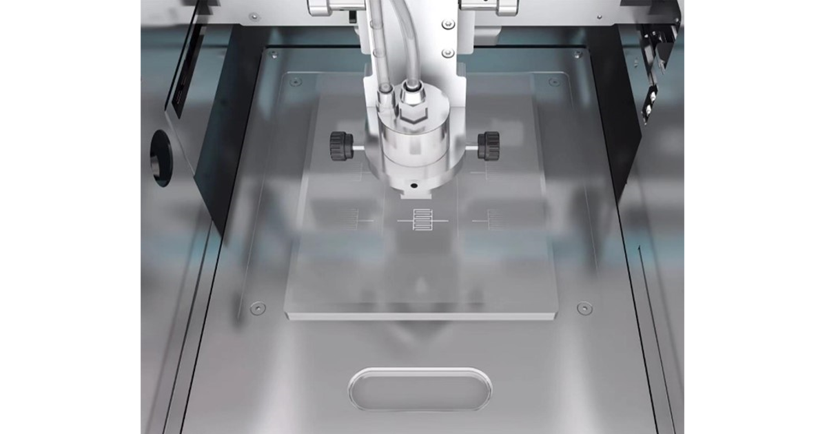
Aerosol jet printing (AJP) is a direct write fabrication technique, with high resolution, design flexibility, and integration capabilities. AJP is capable of printing elaborate material textures on complex, flexible, and stretchable substrates, like fabricating the subtle, intricate electronic and biocompatible sensors, bio-electrodes, antennas, LEDs, RFID tags, 3D interconnects, and even micro-coils for electronic packaging. Specifically, AJP possesses the potential to enable novel and efficient chip packaging solutions on ceramic substrates, such as low-loss micro-strip lines (MSLs) printing to achieve high connectivity, and multi-material microwave package printing with compatible passive and active components.
However, excellent circuits printing performances require material compatibility, process optimization, and fabrication reliability. Appropriate ink selection leads to excellent adhesion, wetting, and compatibility with the targeted substrate, fulfilling the electrical, mechanical, and thermal requirements. Moreover, ink features, like nozzle size, aerosol flow rate, jetting distance, substrate temperature, and relative humidity, largely affect the jetting, deposition, and curing processes, determining the printing accuracy and uniformity. Furthermore, complex geometrical and multi-functional circuits on ceramic substrates depend on the performance of reliable resistance, capacitance, inductance, voltage, current, etc. Therefore, printed circuit post-testing, such as annealing, sintering, and coating, is critical to evaluate the circuits performance, enhancing the fabrication reliability.
Hence, the Special Issue focuses on a collection of original and review articles related to ink technique studies, process parameter optimizations, and post-processing techniques for circuits printing on various substrates. Ingenious and initiative technique applications in chip packaging industry are also welcome.
Potential topics include but are not limited to the following:
- The ink selection with various suspensions and experimental investigations;
- Experimental and theoretical analyses on parameter optimization for printing performances;
- Mechanism analyses of printed ceramics substrates;
- The parameter prediction and optimization of process optimization with machine learning;
- Post-processing and testing techniques for reliability of circuits printing;
- Flexible and stretchable biosensors using AJP;
- Numerical modelling and mechanism analyzing AJP processes.
Prof. Dr. Feng Gu
Prof. Dr. Qingyu Yao
Guest Editors
Manuscript Submission Information
Manuscripts should be submitted online at www.mdpi.com by registering and logging in to this website. Once you are registered, click here to go to the submission form. Manuscripts can be submitted until the deadline. All submissions that pass pre-check are peer-reviewed. Accepted papers will be published continuously in the journal (as soon as accepted) and will be listed together on the special issue website. Research articles, review articles as well as short communications are invited. For planned papers, a title and short abstract (about 100 words) can be sent to the Editorial Office for announcement on this website.
Submitted manuscripts should not have been published previously, nor be under consideration for publication elsewhere (except conference proceedings papers). All manuscripts are thoroughly refereed through a single-blind peer-review process. A guide for authors and other relevant information for submission of manuscripts is available on the Instructions for Authors page. Coatings is an international peer-reviewed open access monthly journal published by MDPI.
Please visit the Instructions for Authors page before submitting a manuscript. The Article Processing Charge (APC) for publication in this open access journal is 2600 CHF (Swiss Francs). Submitted papers should be well formatted and use good English. Authors may use MDPI's English editing service prior to publication or during author revisions.
Keywords
- smart process optimization
- surface engineering
- substrates
- nano/micro lamination fabrication
- chip packaging applications
Benefits of Publishing in a Special Issue
- Ease of navigation: Grouping papers by topic helps scholars navigate broad scope journals more efficiently.
- Greater discoverability: Special Issues support the reach and impact of scientific research. Articles in Special Issues are more discoverable and cited more frequently.
- Expansion of research network: Special Issues facilitate connections among authors, fostering scientific collaborations.
- External promotion: Articles in Special Issues are often promoted through the journal's social media, increasing their visibility.
- e-Book format: Special Issues with more than 10 articles can be published as dedicated e-books, ensuring wide and rapid dissemination.
Further information on MDPI's Special Issue polices can be found here.