Abstract
In this study, we theoretically study the optical bistability (OB) of reflected light beams at visible light frequencies by using a Kretschmann–Raether (KR) configuration where double-layer MoS2 is inserted. This OB phenomenon results from the local field enhancement owing to the excitation of metal surface plasmon polaritons (SPPs) and the introduction of the double-layer MoS2. By considering the third-order conductivity of MoS2, we obtain a threshold electric field with an incident electric field of 107 V/m levels. Furthermore, the influences of the structural parameters on the hysteretic behavior as well as the threshold of OB are clarified. This tunable OB phenomenon will provide possible options for nonlinear optical bistable devices.
1. Introduction
Optical bistability (OB) generally refers to the nonlinear multivalue phenomenon similar to a hysteresis loop between reflected light intensity or transmitted light intensity and incident light intensity in a nonlinear optical system [1]. It has two stable states, which can be dynamically converted by optical signals. Therefore, it is widely used in many fields such as all-optical logic gate [2], all-optical switching [3], optical storage [4], and optical transistor [5]. It is known that the generation of OB phenomenon requires the introduction of the nonlinear optical properties of materials. However, because the nonlinear coefficient of traditional materials is generally small, optical bistable devices often need a large size or strong incident light intensity in order to obtain an obvious OB phenomenon when preparing optical bistable devices. This fundamentally limits the practical application of OB devices. With the development of micro–nano technology and the practical demand for integrated all-optical devices, on the one hand, people are seeking low-threshold OB solutions in various micro–nano structures, such as photonic crystal nanocavities [3], Fabry Perot cavities [6], metamaterials [7], dielectric grates [8], etc. On the other hand, people are trying to find optical bistable schemes based on large nonlinear coefficients of optical materials. Among them, the Dirac materials represented by two-dimensional graphene is the most representative. Researchers have found that some Dirac materials such as graphene have large third-order nonlinear coefficients [9,10]. This makes them stand out among many optical materials and has attracted the attention of researchers in the field of OB. Taking graphene as an example, in addition to its large nonlinear conductivity characteristics, it also an has ultra-fast response time [11], linear/nonlinear conductivity that is easily dynamically regulated [12], and a wide response bandwidth [13]. These properties make graphene-based micro–nano structures have obvious advantages in achieving low-threshold OB. Xiang et al. first theoretically studied the optical bistable phenomenon at the interface between graphene and a Kerr-type nonlinear substrate [14]. Bao et al. experimentally observed the existence of OB for the first time in a Fabry Perot cavity structure containing a graphene thin layer [15]. The above advantages and the milestone progress make graphene-based low threshold schemes in micro–nano structures become a hot spot of attention. OB in structures such as graphene/waveguide hybrid structures [16], modified Kretschmann–Raether (KR) configurations [17], and multilayer graphene structures [18] have been reported. Although Dirac materials, such as graphene, have advantages in achieving low-threshold OB, there are inevitably limitations. Also take graphene as an example: its third-order nonlinear conductivity decreases sharply with the increase in frequency, so most of the above graphene-based low threshold schemes are concentrated in the terahertz band. The implementation of low-threshold OB schemes in infrared and even visible frequencies is still a challenging task.
In recent years, researchers have found that MoS2 as a Kerr nonlinear medium has begun to emerge in the field of nonlinear optics. MoS2 is one of transition metal dihalide compounds, which has many physical and chemical properties similar to graphene [19]. However, unlike graphene, Dirac semimetal and other materials, MoS2 is a band gap semiconductor material, and its band gap size is closely related to the number of MoS2 layers. With the change in the number of MoS2 layers, its band gap size is also constantly changing, ranging from 1.29 to 1.90 eV [20]. Single-layer MoS2 has a direct band gap when it exists, and double-layer or multi-layer MoS2 has an indirect band gap when it exists, and the band gap can cover the mid-infrared to visible frequencies. In particular, double-layer MoS2 has been found to have appreciable third-order nonlinear coefficients in the visible light band [21]. This creates the conditions for OB to be achieved at visible frequencies and even with low thresholds. Therefore, we cannot help but ask the relevant scientific question: given the practical significance of realizing optical bistable devices in the visible band, can we try to explore the optical bistable phenomenon through the micro–nano structure based on MoS2? To answer this question, in this paper, we design a KR structure based on MoS2 and try to combine the local field enhancement of surface plasmon polaritons (SPPs) and the nonlinear characteristics of double-layer MoS2 in visible light to achieve OB at the lowest possible threshold in the visible light band. The theoretical calculation results show that the structure can realize the reflected type of optical bistable phenomenon with the order of through proper parameter setting. On this basis, we further study the influence of incident wavelength, incident angle, gold thickness, and refractive index of prism on OB behavior. Considering the simple structure and easy preparation of the scheme, we believe it may provide a basic reference for the practical application of nonlinear optical devices such as all-optical switches and all-optical logic gates based on OB.
2. Theoretical Model and Method
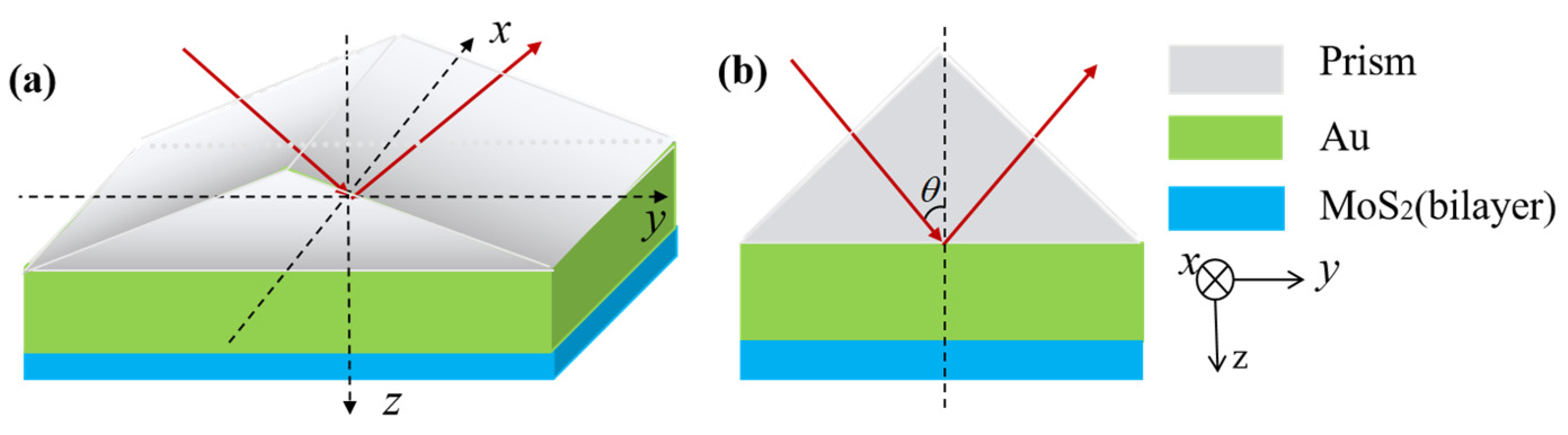
We consider a typical KR structure capable of exciting SPPs, as shown in Figure 1. This structure is composed of a coupling prism, a gold layer, and a double-layer MoS2 from top to bottom. We assume that the incident light enters from one side of the prism and the incident wavelength is 468 nm. The contact surface between the prism and the gold layer coincides with the plane formed by the x-axis and y-axis. The TM polarization light in the yz plane is the incident on the contact surface inside the prism. The coupling prism and the gold layer constitute the basic KR structure for the excitation of SPPs. Here the refractive index of the coupling prism is set to . A gold layer with an initial thickness of
is placed at the lower end of the prism, and its dielectric constant can be expressed by the Drude–Lorentz model as [22]:
where is the wavelength of incident light, and and denote the plasma wavelength and collision wavelengths, respectively. Their values are , , respectively. The lowest layer of MoS2 is used to provide nonlinear optical properties conditions for the generation of OB phenomenon. It should be noted that the single-layer MoS2 only has a direct band gap, and double-layer or multi-layer MoS2 has indirect band gap. Consequently, we use the double-layer MoS2 under the gold layer in the diagram of Figure 1. The dielectric constant of MoS2 can be expressed as [23]
where is the direct-current dielectric constant, and
represents the oscillator strength (specific values are as follows: , , , , , ).
represents the damping coefficient (specific values are as follows: rad/s, rad/s, rad/s, rad/s, rad/s, rad/s).
represents the response frequency (specific values are as follows: rad/s, rad/s, rad/s, rad/s, rad/s, rad/s). rad/s is the plasma frequency. DawsonF represents the Dawson’s Function. , , and represent the maximum value, mean, and variance of a typical Gaussian distribution function, respectively. Their values are eV, eV, respectively.
is the reduced Planck constant. On this basis, the first-order linear conductivity and third-order nonlinear conductivity of double-layer MoS2 can be expressed by its dielectric constant as [21]
where is the thickness of MoS2,
is the wave vector in the vacuum, is the vacuum resistivity,
is the mass of an electron, is the centrality frequency with ,
is of the order of the dimensions of an atom (),
is the atomic number density with , is the permittivity of vacuum, is the electron charge [24]. Based on the above linear and nonlinear conductivity, the total conductivity of MoS2 can be expressed as
where is the local electric field at the double-layer MoS2.
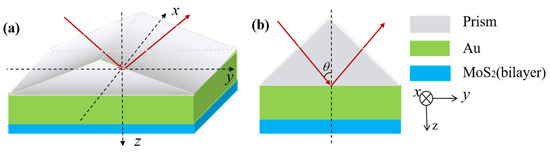
Figure 1.
Schematic diagram of KR structure based on double-layer MoS2. (a) is a perspective view, and (b) is a side view.
It is known that SPPs can only be excited under TM polarization. Therefore, we only consider the case of TM polarization for the calculation of OB. In the case of TM polarization, based on Maxwell’s equations, the propagation of electromagnetic waves through a coupling prism can be expressed as
the propagation of electromagnetic fields in gold layer can be expressed as
and the propagation of the electromagnetic field in the outgoing medium (air) can be expressed as
where , , and represents the amplitudes of the incident magnetic field, the transmitted magnetic field, and the reflected magnetic field, respectively. , , and , respectively, represent wave vectors in vacuum, wave vectors in the coupling prism, and wave vectors in the gold layer. At the interface between the gold and bottom-layer air medium, there are boundary conditions and . By combining (7) and (8), we can obtain
At the interface between the coupling prism and gold layer, the boundary conditions are different, and , due to the presence of a thin layer of MoS2. By combining (6) and (7), we obtain
here, and represent the forward and reverse magnetic fields of the electromagnetic wave traveling along the z axis, respectively. By eliminating and in simultaneous (10), the incident magnetic field and reflected magnetic field can be expressed by the transmitted magnetic field at the same time:
For ease of representation, some complex expressions are represented by a simple letter:
Let , , . By eliminating simultaneously (11)–(13), the functional relationship between the incident magnetic field and the reflected magnetic field can be directly obtained:
Then, by substituting the electromagnetic field relation into (15), the functional relation between the incident magnetic field and the reflected magnetic field can be converted into the relation between the incident electric field and the reflected electric field .
3. Results and Discussions
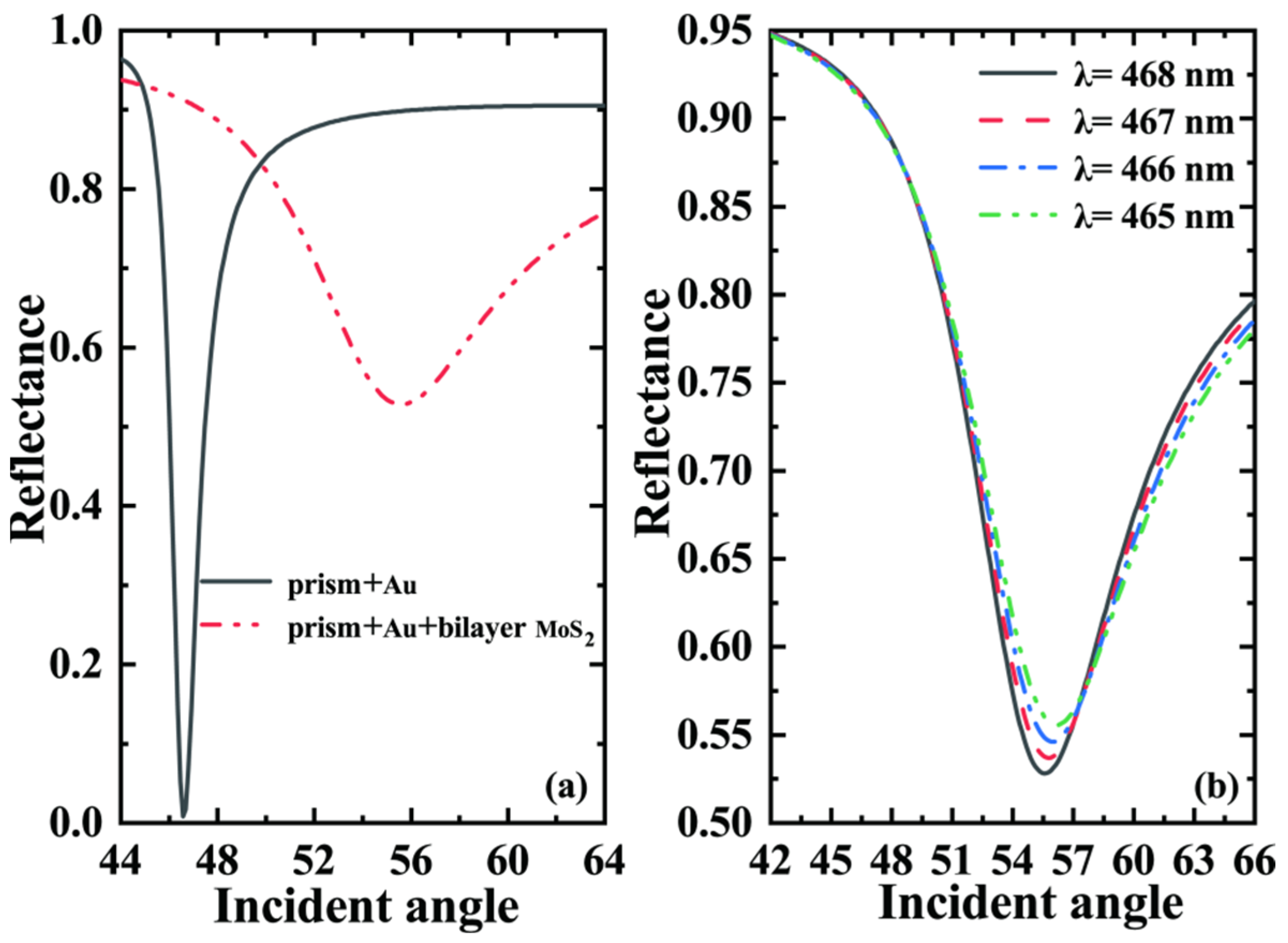
In this section, we discuss in detail the influence of double-layer MoS2 on SPPs and the OB phenomenon. First, we calculated the reflectance of the whole structure in Figure 1 with the incident angle based on the classical transfer matrix method, as shown in Figure 2a. From the reflectance curve in Figure 2a, it can be clearly found that the structure of the coupling prism and the gold layer causes a small, reflected peak in the reflectance at of the incident angle. This reflected peak means that SPPs on the gold-layer surface are excited. This is a very mature SPP excitation phenomenon, and there is no need to go into details here. The excitation of SPPs is often accompanied by significant local field enhancement. The E-field distribution plots can not only visually display the local field enhancement phenomenon caused by SPPs excitation, but also provide theoretical support for the generation of a low-threshold OB phenomenon. Considering that the E-field distribution plots in KR structures are very mature and predictable, we do not redraw the E-field distribution plots here. People can see the E-field distribution plots from our previous work [25]. In addition, as the double-layer MoS2 is placed under the gold layer, the excitation angle of SPPs shifts significantly to the right, and the minimum reflectance of the double-layer MoS2 rises from near zero to 0.52, as shown by the red dashed line in Figure 2a. It is not difficult to understand that because the thickness of double-layer MoS2 is nearly zero and it has a large conductivity, its addition is essentially equivalent to the introduction of a large loss in the structure, so that the lowest value of the reflectance has changed. On the basis of keeping the other parameters unchanged, we further discuss the variation law of the reflectance with the angle when only the incident wavelength is changed, and the results are shown in Figure 2b. It can be found that the minimum value of the reflected peak decreases slightly with the increasing of the incident wavelength, and there is a slight tendency to move to a lower angle. The main reason for this trend is that the conductivity of MoS2 is a function of wavelength change. According to Formulas (2)–(5), the first-order, third-order, and total conductivity of MoS2 can be adjusted by the vacuum wave vector , and itself can be regulated by the incident wavelength, so we can indirectly control the conductivity of MoS2 by controlling the incident wavelength. Since many practical laser sources have the function of wavelength regulation in a certain band range, the incident wavelength can be used as an important scheme of OB dynamic regulation.
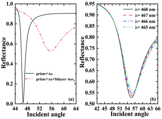
Figure 2.
(a) Curve of reflectance and incident angle, where the incident wavelength is . (b) The variation in reflectance with incident angle at different incident wavelengths.
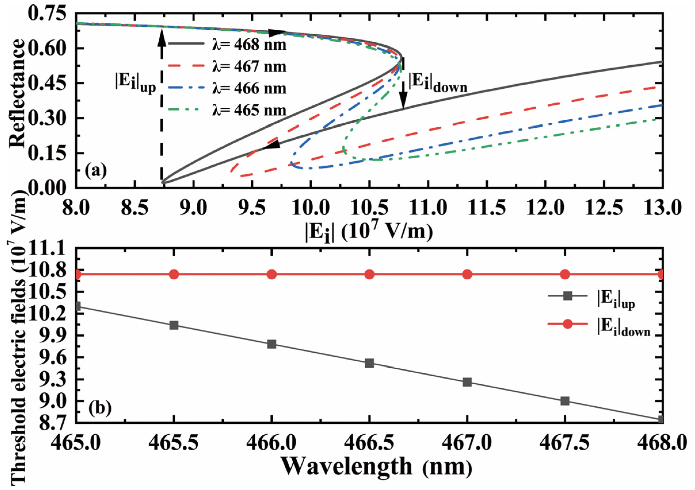
Based on the excitation of SPPs in Figure 2, we continue to discuss the reflected OB phenomenon in the coupling prism structure containing double-layer MoS2. From Formula (4), it can be seen that double-layer MoS2 demonstrated a large third-order nonlinear conductivity in the visible band, which provides nonlinear conditions for the realization of OB in the visible band. At the same time, the excitation of SPPs between the prism and the gold layer makes the MoS2 region present obvious local field enhancement effect. This also provides positive conditions for further lowering the threshold of OB. According to Formula (5), the increase in the local electric field near MoS2 can enhance the nonlinear conductivity of MoS2. This enables MoS2 to obtain a more obvious and stronger nonlinear response under the same incident light intensity, which is conducive to the appearance of OB phenomenon and the reduction in the OB threshold. In order to obtain a suitable bistable reflectance curve, based on the rule in Figure 2, we set the initial incident angle as , and kept the other parameters consistent with Figure 2. After adopting the calculation method of OB in the previous part and undergoing program debugging and parameter optimization, we obtained the relationship curve between the reflectance and incident electric field, and the results are shown in Figure 3a. It is not difficult to find from the figure that the introduction of double-layer MoS2 makes the linear reflected peak in Figure 2 show an inverse “S” shape, changing the hysteresis curve with the change in the incident electric field, which means the occurrence of an OB phenomenon. Let us take the curve corresponding to as an example for discussion. When the incident electric field slowly increases from a lower value, the reflectance curve slowly decreases to one of the “stable states”. This situation corresponds to the upper part of the curve and is described by the arrow pointing to the right as the trend of reflectance changes with the incident electric field. If the incident electric field continues to increase and reaches the downward threshold electric field , at this time, the reflectance suddenly experiences a “jump”, causing the reflectance to “jump” to the curve in the lower right corner with the change in the incident electric field. This means that once the increase in the incident electric field exceeds the threshold, it achieves a transition from one “stable state” to another. Similarly, when the incident electric field slowly decreases from a higher value, the reflectance curve slowly decreases to one of the “stable states”. This situation corresponds to the lower part of the curve and is described by the arrow pointing to the left to indicate the trend of reflectance variation with the incident electric field. If the incident electric field continues to decrease and reaches the upward threshold electric field , at this time, the reflectance suddenly undergoes a “jump”, causing the reflectance to “jump” to the curve in the upper left corner with the change in the incident electric field. This also means that once the reduction in the incident electric field exceeds the threshold, it achieves a transition from one “stable state” to another. The “middle” part of the inverse “S” shape curve is actually “unstable”. That is to say, as the incident electric field gradually increases or decreases, the reflectance curve (or reflected electric field) will not change along the “middle” part of the inverse “S” shape curve. The threshold for steady-state jumps also appears in the order of . In general, we refer to the electric field of
as the low threshold, and there are many efforts to achieve this threshold in the terahertz band. However, because the bistable phenomenon appears in the visible light band, the threshold is not too high, which is relatively rare. Figure 3a further shows the relationship between the reflectance curve of the structure at different incident wavelengths and the incident electric field on the basis of Figure 2. It also provides a way to dynamically regulate the OB curve. With the increase in incident wavelength, we find the upper threshold () of OB gradually decreases, while the lower threshold () is almost unchanged, which results in the widening of threshold width () with the increase in wavelength. In order to show this rule more intuitively, we also drew the value curves of the upper threshold and lower threshold of OB at different incident wavelengths, and the results are shown in Figure 3b. The change in incident wavelength can lead to a change in the upper and lower thresholds of OB, which play a dynamic regulating role on the threshold width of OB. For example, when the incident wavelength is , the upper threshold of OB is , the lower threshold is , and the threshold width is When the incident wavelength is , the upper threshold of OB is , the lower threshold is , and the threshold width becomes . Further, when the incident wavelength is , the OB’s upper threshold , lower threshold , and the threshold width can be dynamically adjusted by adjusting the incident wavelength, and the associated OB threshold and threshold width can also be flexibly controlled within a certain range. This provides a reference way for realizing flexible and controllable optical bistable devices.
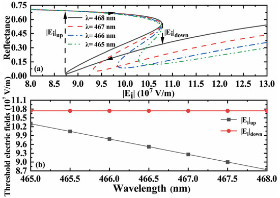
Figure 3.
(a) The relationship between reflectance and incident electric field at different incident wavelengths. (b) The relationship between the upper and lower thresholds of OB with the incident wavelength.
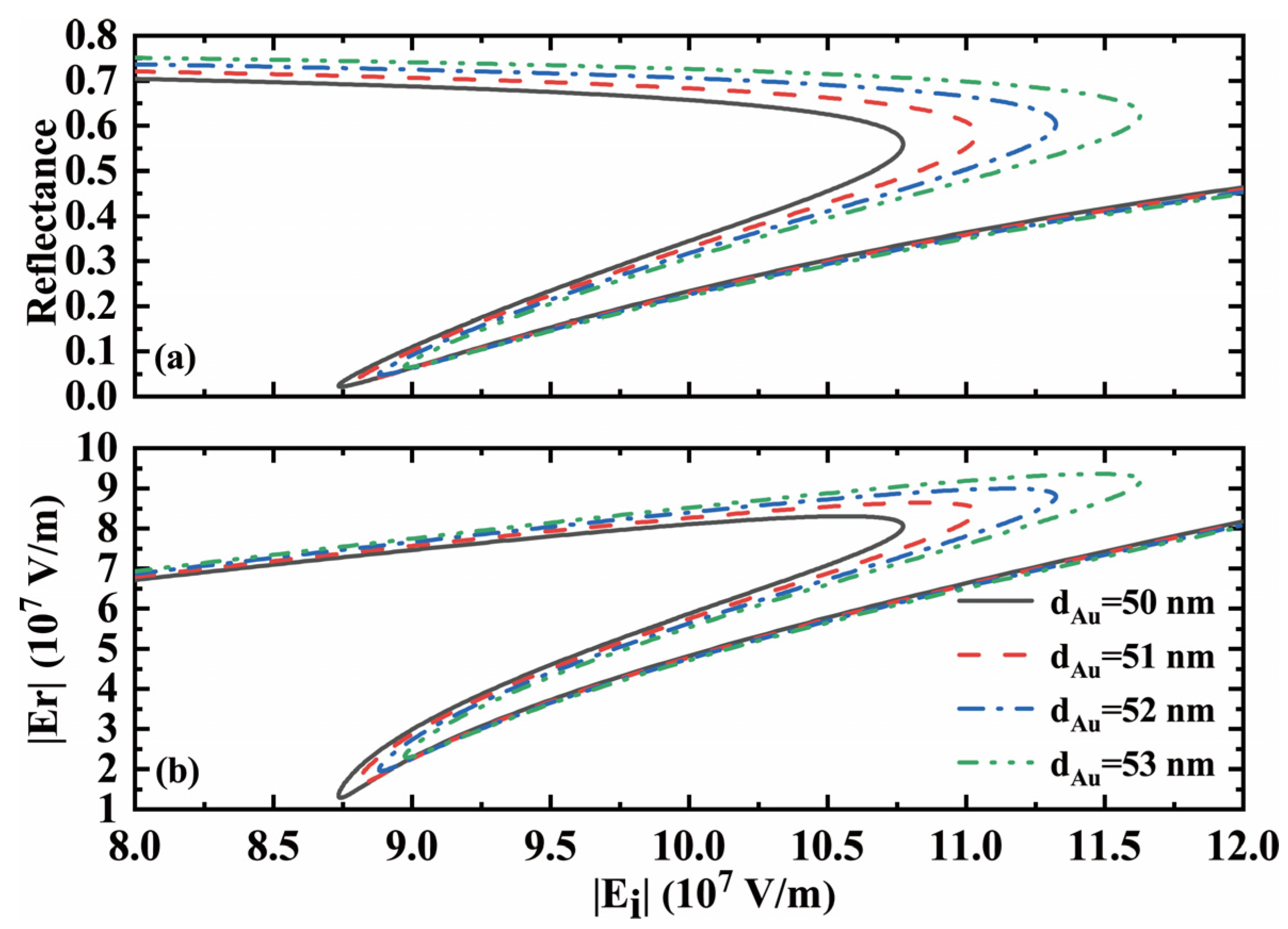
Considering that the thickness of the gold layer may be slightly deviated under different processes and technologies during the preparation of actual bistable devices, it is necessary to clarify the influence of the thickness of the gold layer on the OB phenomenon. In mechanism, the change in gold layer thickness can change the dispersion curve of SPPs and indirectly affect the OB phenomenon. Next, we calculated the relation between reflectance and the reflected electric field with incident electric field for different thicknesses of the gold layer, as shown in Figure 4a,b. The results show that a slight change in gold layer thickness can also have a detailed change in OB behavior. With the increase in the thickness of the gold layer, the upper threshold of OB gradually increases, and the lower threshold also gradually increases. However, the increase speed of the lower threshold of OB is greater than the increase speed of the upper threshold, which leads to the widening of the threshold width of OB. For example, when the thickness of the gold layer is , the upper threshold value of OB is , the lower threshold value is , and the threshold width is When the gold layer thickness is , the upper threshold value of OB changes to , the lower threshold value changes to , and the threshold width changes to . It is obvious that the change in the thickness of the gold layer has a certain effect on OB behavior. We have compiled the changes in this parameter in Table 1 for easy comparison. By gradually reducing the thickness of the gold layer, an OB with a larger threshold width can be obtained, which not only provides a new idea for the realization of tunable OB, but also provides a reference for the possible changes in the OB phenomenon caused by the imprecision of the thickness of the gold layer caused by the actual preparation process.
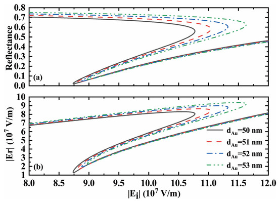
Figure 4.
Changes in reflectance (a) and reflected electric field (b) with incident electric field under different gold thicknesses, and other parameters are the same as those in Figure 1.

Table 1.
Comparison of the threshold with different parameters.
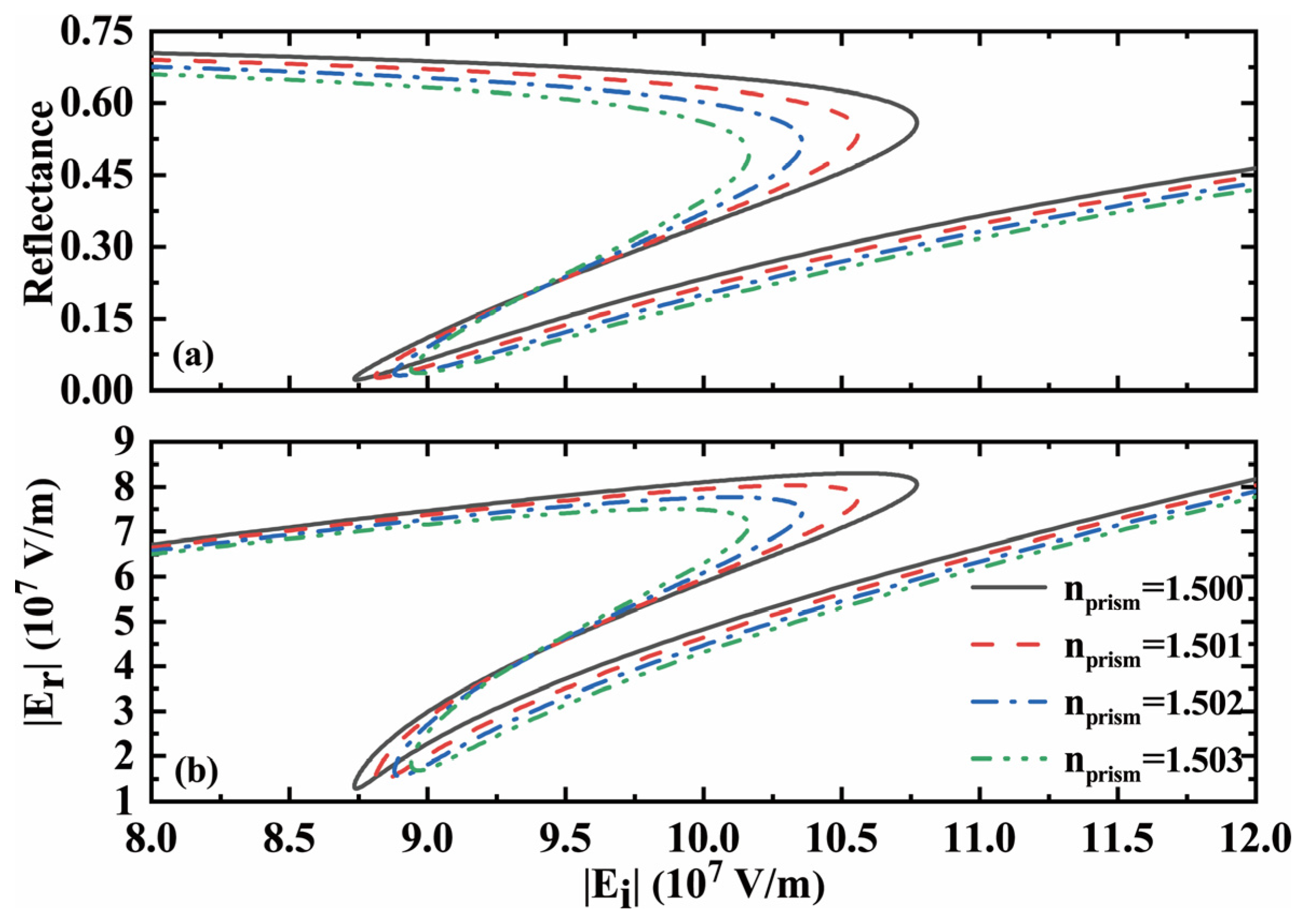
Next, we briefly discuss the influence of the refractive index of coupling prism on OB behavior. This is mainly because the coupling prism is an important component of the system, and the slight change in its refractive index can also affect the excitation of SPPs, thus affecting the hysteresis behavior of OB. Based on this, we use the same calculation method as before to draw the curve of reflectance and reflected electric field with the incident angle, as shown in Figure 5a,b. It is not difficult to find from the figure that a slight increase in the refractive index of the coupling prism can gradually increase the upper threshold value of OB, while the lower threshold value gradually decreases, which leads to a decrease in the threshold width of OB. For example, when , the upper threshold of OB is , the lower threshold is , and the threshold width is When , the upper threshold of OB is , the lower threshold is , and the threshold width is adjusted to We have also compiled the changes in this parameter in Table 1 for easy comparison. Theoretically, it seems that the refractive index of the coupling prism can also be used as a way to dynamically regulate OB. However, this regulation law can only be used as a reference and cannot provide dynamic regulation in the actual situation. This is mainly because once the coupling prism is prepared, its refractive index does not have the property of dynamic change. Nevertheless, it is equally positive to explore its impact on the OB phenomenon.
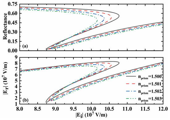
Figure 5.
The relationship between reflectance (a) and reflected electric field (b) with incident electric field under different refractive indices of coupling prism. The other parameters are consistent with those shown in Figure 1.
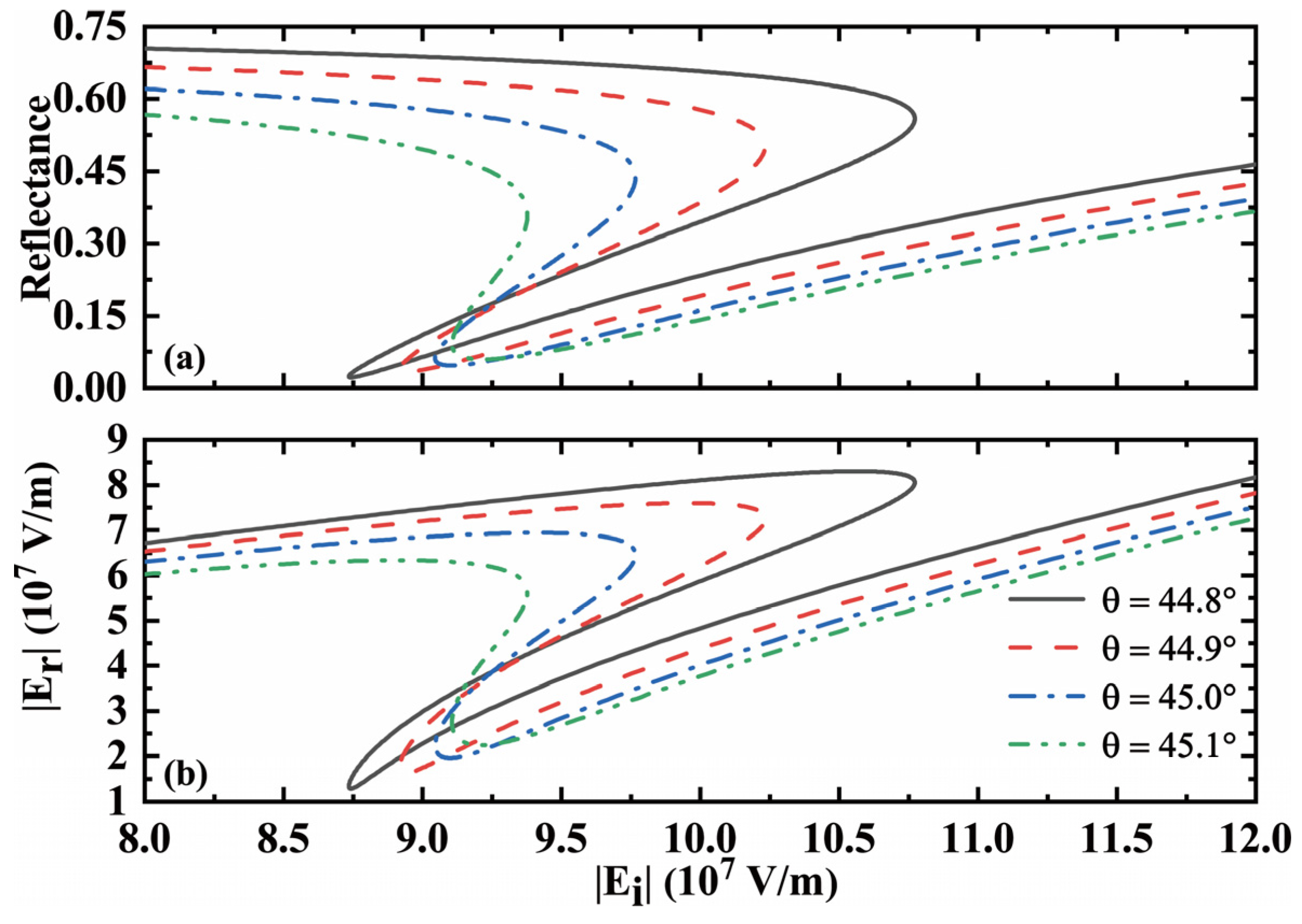
Due to the fact that the incident angle directly affects the wave vector in the propagation direction, there may indeed be slight deviations in the incident angle during actual experimental operations. This makes it equally necessary to discuss the impact of the changes in incident angle on OB. Finally, we considered the impact of subtle changes in the incident angle on OB behavior, as shown in Figure 6a,b. As expected, the hysteresis curve of OB is sensitive to subtle changes in the incident angle, similar to the effect of incident wavelength on OB. As the incident angle slowly increases, the upper threshold of OB gradually increases, while the lower threshold gradually decreases, resulting in a significant decrease in the threshold width of OB. The continuous increase in the incident angle can even cause the hysteresis curve to disappear and the OB phenomenon to be lost. However, this does not mean that a smaller incident angle is better. Although the lower incident angle can reduce the threshold value of OB to a certain extent, it can also make the incident angle gradually deviate from the resonance angle of SPPs becoming even lower than the total reflection angle, so that the positive effect of SPPs excitation on OB can be reduced or even disappear. Based on the above discussion, it is not difficult to find the OB scheme with optimal design performance is the result of comprehensive balance and compromise of various structural parameters and material parameters.
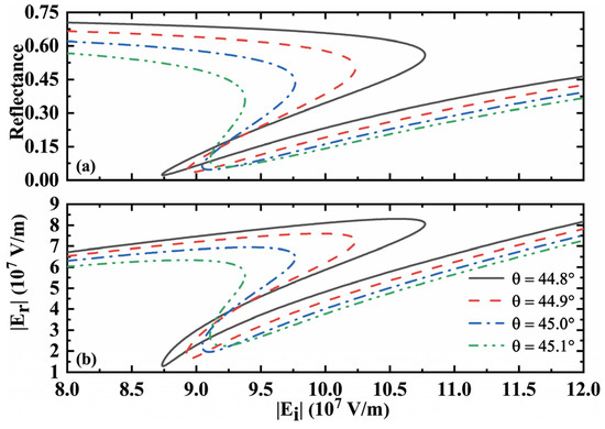
Figure 6.
Relation between reflectance (a), reflected electric field (b) and incident electric field at different incident angles. Other parameters remain the same as before.
4. Conclusions
In conclusion, we achieved a relatively low-threshold OB in the visible light by combining a double-layer MoS2 with a simple KR structure that excites SPPs. The large third-order nonlinear conductivity of double-layer MoS2 provides the supporting conditions for the appearance of OB in the visible band. The analytical expression between the incident electric field and reflected electric field is obtained based on the derivation of the relation with the electromagnetic field. In addition, through the optimization of structural and material parameters, we also obtained a reflected OB with an electric field of order in the visible band. The OB is realized because of the large third-order nonlinear conductivity of double-layer MoS2 in the visible light and the local field enhancement caused by the excitation of SPPs at the gold–prism interface. This work provides a new idea for the realization of low-threshold OB in the visible light band, and also provides a reference scheme for the design and implementation of practical OB devices in optical communication bands. Given the simple structure and ease of preparation of the scheme, we believe that it is possible to find potential applications in all-optical modules in optical communications.
Author Contributions
H.T. and L.J.; Writing—original draft, H.T. and S.T.; Formal analysis, H.W. and J.Z.; Supervision, G.S. All authors have read and agreed to the published version of the manuscript.
Funding
This work is supported by the China State Key Laboratory of Complex Electromagnetic Environment Effects on Electronic and Information System (CEMEE2022K0302A); the Hunan Provincial Natural Science Foundation of China (2022JJ40280).
Institutional Review Board Statement
Not applicable.
Informed Consent Statement
Not applicable.
Data Availability Statement
Data are contained within the article.
Conflicts of Interest
The authors declare that they have no known competing financial interests or personal relationships that could have appeared to influence the work reported in this paper.
References
- Gibbs, H.M. Optical Bistability: Controlling Light with Light; Academic Press: Orlando, FL, USA, 1985. [Google Scholar]
- Zhang, W.L.; Jiang, Y.; Zhu, Y.Y.; Wang, F.; Rao, Y.J. All-optical bistable logic control based on coupled tamm plasmons. Opt. Lett. 2013, 38, 4092–4095. [Google Scholar] [PubMed]
- Notomi, M.; Shinya, A.; Mitsugi, S.; Kira, G.; Tanabe, T. Optical bistable switching action of Si high-Q photonic-crystal nanocavities. Opt. Express 2005, 13, 2678–2687. [Google Scholar] [PubMed]
- Tanabe, T.; Notomi, M.; Mitsugi, S.; Shinya, A.; Kuramochi, E. Fast bistable all-optical switch and memory on a silicon photonic crystal on-chip. Opt. Lett. 2005, 30, 2575–2577. [Google Scholar] [PubMed]
- Yanik, M.F.; Fan, S.; SoljaciÄ, M.; Joannopoulos, J.D. All-optical transistor action with bistable switching in a photonic crystal cross-waveguide geometry. Opt. Lett. 2003, 28, 2506–2508. [Google Scholar] [PubMed]
- Yuan, H.; Jiang, X.; Huang, X.; Sun, X. Ultralow threshold optical bistability in metal/randomly layered media structure. Opt. Lett. 2016, 41, 661–664. [Google Scholar] [PubMed]
- Myunghwan, K.; Sangin, K.; Soeun, K. Optical bistability based on hyperbolic metamaterials. Opt. Express 2018, 26, 11620–11632. [Google Scholar]
- Litchinitser, N.M.; Gabitov, I.R.; Maimistov, A.I. Optical bistability in a nonlinear optical coupler with a negative index channel. Phys. Rev. Lett. 2007, 99, 113902. [Google Scholar] [PubMed]
- Zhang, H.; Stéphane, V.; Bao, Q.; Kian Ping, L.; Massar, S.; Godbout, N. Z-scan measurement of the nonlinear refractive index of graphene. Opt. Lett. 2012, 37, 1856–1858. [Google Scholar] [PubMed]
- Kotov, O.V.; Lozovik, Y.E. Dielectric response and novel electromagnetic modes in three-dimensional dirac semimetal films. Phys. Rev. B 2016, 93, 235417. [Google Scholar]
- Chen, J.H.; Jang, C.; Xiao, S. Intrinsic and extrinsic performance limits of graphene devices on SiO2. Nat. Nano 2008, 3, 206–209. [Google Scholar]
- Li, Z.Q.; Henriksen, E.A.; Jiang, Z.; Hao, Z.; Martin, M.C.; Kim, P. Dirac charge dynamics in graphene by infrared spectroscopy. Nat. Phys. 2008, 4, 532–535. [Google Scholar]
- Bonaccorso, F.; Sun, Z.; Hasan, T.; Ferrari, A.C. Graphene photonics and optoelectronics. Nat. Photonics 2010, 4, 611–622. [Google Scholar]
- Xiang, Y.; Dai, X.; Guo, J.; Wen, S.; Tang, D. Tunable optical bistability at the graphene-covered nonlinear interface. Appl. Phys. Lett. 2014, 104, 3760–3763. [Google Scholar]
- Bao, Q.; Chen, J.; Xiang, Y.; Zhang, K.; Li, S.; Jiang, X. Graphene nanobubble: A new optical nonlinear material. Adv. Opt. Mater. 2015, 3, 744–749. [Google Scholar]
- Deng, H.; Ji, C.; Zhang, X.; Chen, P.; Jiang, L. Low threshold optical bistability in graphene/waveguide hybrid structure at terahertz frequencies. Opt. Commun. 2021, 499, 127282. [Google Scholar]
- Dai, X.; Jiang, L.; Xiang, Y. Low threshold optical bistability at terahertz frequencies with graphene surface plasmons. Sci. Rep. 2015, 5, 12271. [Google Scholar]
- Guo, L.; He, Y.; Cheng, Y.; Yin, C. Controllable transition between optical bistability and multistability in graphene/dielectric/graphene structure. Eur. Phys. J. B 2018, 91, 79. [Google Scholar]
- Butler, S.Z.; Hollen, S.M.; Cao, L.; Cui, Y.; Gupta, J.A.; Gutiérrez, H.R. Progress, challenges, and opportunities in two-dimensional materials beyond graphene. ACS Nano 2013, 7, 2898–2926. [Google Scholar]
- Mak, K.F.; Lee, C.; Hone, J.; Shan, J.; Heinz, T.F. Atomically Thin MoS2: A new direct-gap semiconductor. Phys. Rev. Lett. 2010, 105, 136805. [Google Scholar]
- Balaei, M.; Karimzadeh, R.; Naseri, T. Introducing a novel approach to linear and nonlinear electrical conductivity of MoS2. Opt. Mater. Express 2021, 11, 2665–2674. [Google Scholar]
- Maharana, P.K.; Jha, R. Chalcogenide prism and graphene multilayer based surface plasmon resonance affinity biosensor for high performance. Sens. Actuators B Chem. 2012, 169, 161–166. [Google Scholar]
- Shen, C.C.; Hsu, Y.T.; Li, L.J.; Liu, H.L. Charge dynamics and electronic structures of monolayer MoS2 films grown by chemical vapor deposition. Appl. Phys. Express 2013, 6, 125801. [Google Scholar]
- Mukherjee, B.; Tseng, F.; Gunlycke, D.; Amara, K.K.; Eda, G.; Simsek, E. Complex electrical permittivity of the monolayer molybdenum disulfide (MoS2) in near UV and visible. Opt. Mater. Express 2015, 5, 447–455. [Google Scholar]
- Jiang, L.; Guo, J.; Wu, L.; Xu, H.; Dai, X.; Xiang, Y. Perfect terahertz absorption with graphene surface plasmons in the modified otto configuration. Plasmonics 2017, 12, 1825–1831. [Google Scholar]
Disclaimer/Publisher’s Note: The statements, opinions and data contained in all publications are solely those of the individual author(s) and contributor(s) and not of MDPI and/or the editor(s). MDPI and/or the editor(s) disclaim responsibility for any injury to people or property resulting from any ideas, methods, instructions or products referred to in the content. |
© 2024 by the authors. Licensee MDPI, Basel, Switzerland. This article is an open access article distributed under the terms and conditions of the Creative Commons Attribution (CC BY) license (https://creativecommons.org/licenses/by/4.0/).