
Crack-Templated Patterns in Thin Films: Fabrication Techniques, Characterization, and Emerging Applications


Abstract
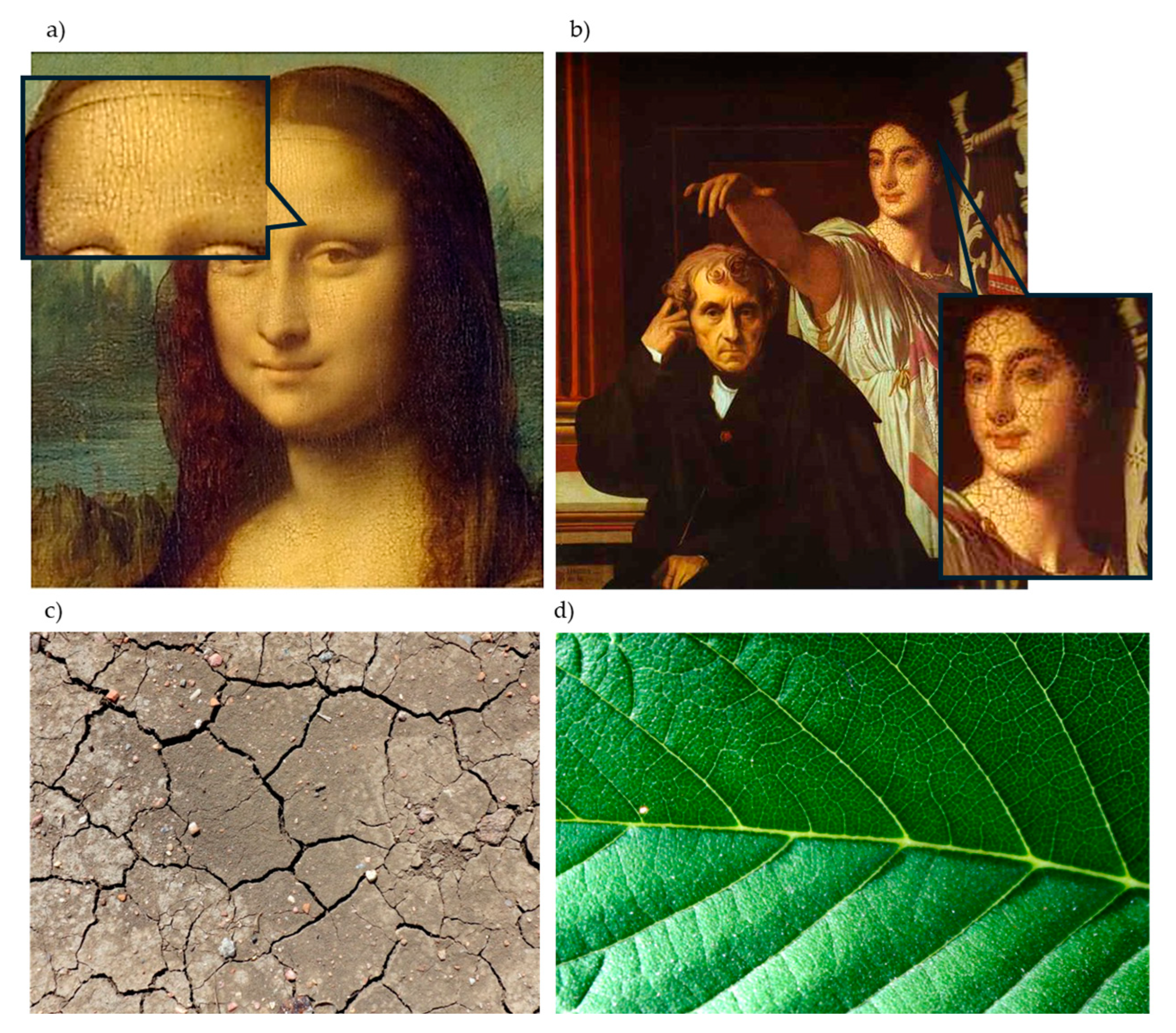
:1. Introduction
2. Crack Templating
2.1. Concept and Mechanism of Crack Formation
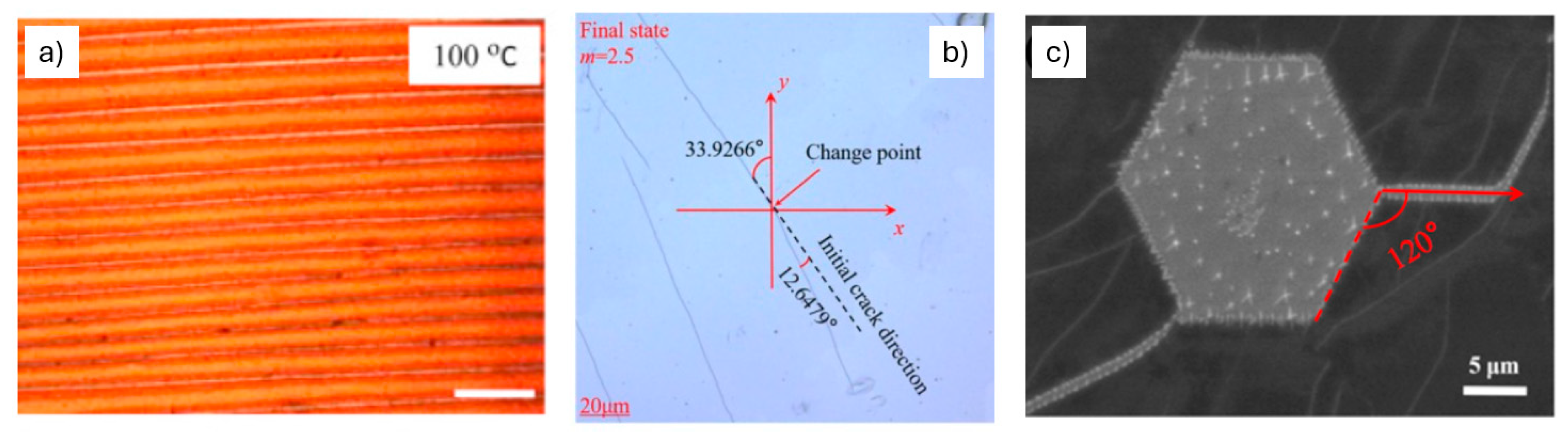
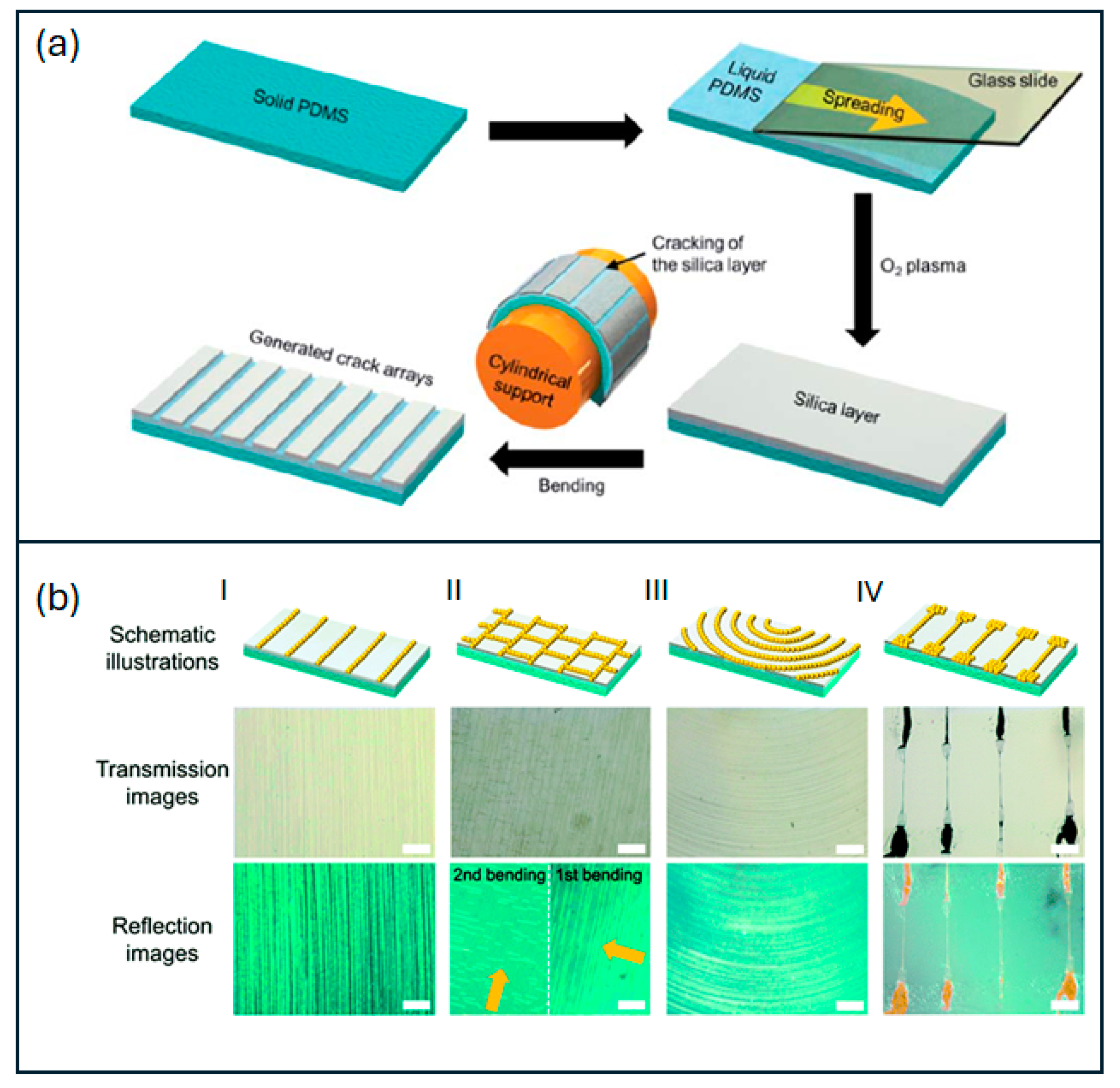
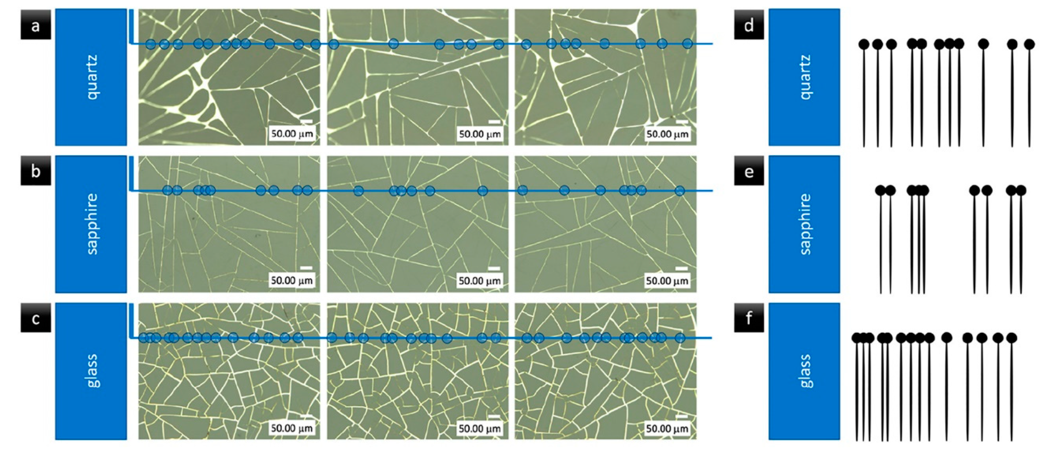
2.2. Orientation and Morphology
3. Materials for Crack Template Fabrication
3.1. Bio-Based Materials
3.2. Ceramic-Based Materials
3.3. Polymeric, Hybrid, and Composite Materials
4. Preparation Techniques for Crack-Templated Thin Films
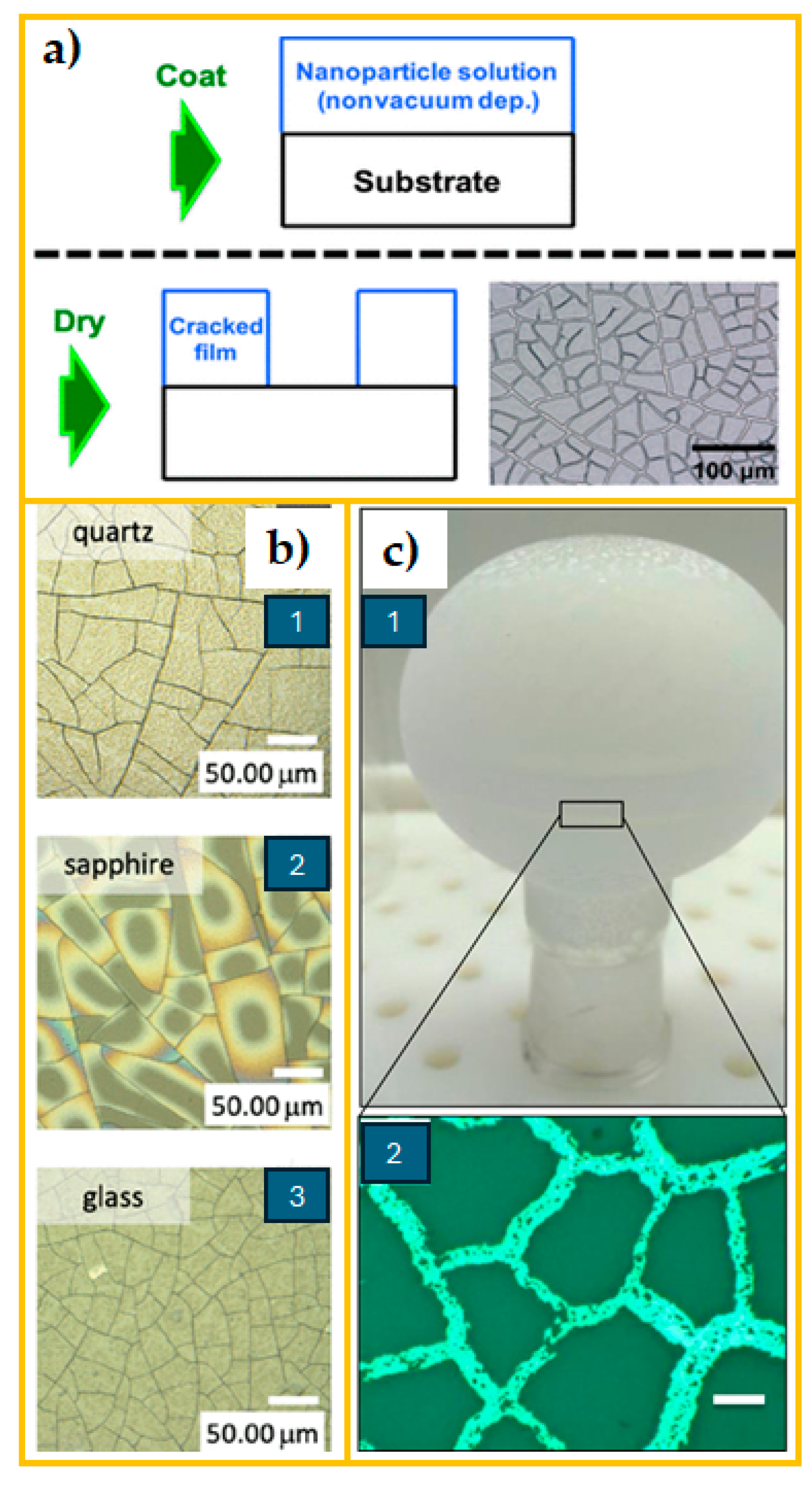
4.1. Deposition Techniques
- Spin coating: a high-speed technique where a liquid solution is evenly distributed over the substrate through centrifugal force [26,56]. Tunable parameters: solution viscosity, spin speed, spin time, and substrate surface energy. These factors influence film thickness, uniformity, and drying rate, thereby affecting crack density and morphology.
- Drop coating: a straightforward approach where droplets of the solution are deposited onto the substrate and allowed to spread and dry, forming crack networks [14]. Tunable parameters: droplet volume, deposition position, solution concentration, drying environment (temperature and humidity), and substrate inclination. These parameters dictate the spreading dynamics and final crack distribution.
- Blade coating: a method in which a solution is spread across the substrate using a blade or knife, enabling controlled film thickness over large areas [54]. Tunable parameters: blade speed, solution viscosity, blade height, substrate temperature, and drying atmosphere. These settings determine the uniformity, thickness, and drying kinetics, which directly affect crack formation.
- Dip coating: in this technique, a substrate is immersed into a solution and then withdrawn at a controlled speed. As the solvent evaporates, a thin film forms on the substrate surface, which develops cracks due to stresses induced during drying or shrinkage. Additionally, biphasic dip coating can also be exploited to induce the self-ordering of the cracks, by using an immiscible second solvent [66]. Tunable parameters: withdrawal speed, solution viscosity, immersion time, drying conditions (temperature, humidity, and airflow), and solution composition.
- Spray coating: a versatile deposition method used to create crack templates by atomizing a solution into fine droplets and spraying them onto a substrate. This method is particularly advantageous for coating large areas, irregular surfaces, or substrates with complex geometries [58]. Tunable parameters: spray nozzle specifications, spray pressure, solution flow rate, substrate distance from the nozzle, spray angle, drying conditions (temperature, humidity, airflow), solution composition (solute-to-solvent ratio, solvent volatility), and substrate properties.
- Electron beam evaporation: a physical vapor deposition technique where a high-energy electron beam is used to evaporate a source material, typically in a vacuum chamber. The vaporized material condenses on the substrate, forming a thin film. Cracks can form due to thermal stresses induced by differences in the thermal expansion coefficients of the substrate and deposited film [11]. Tunable parameters: electron beam energy, deposition rate, vacuum pressure, substrate temperature, material properties of the source and substrate, and post-deposition annealing conditions.
4.2. Solvent Evaporation
4.3. Thermal Stress Induction
4.4. Mechanical Stretching
4.5. UV Curing
5. Process Parameters Governing Tunable Features of Crack Patterns
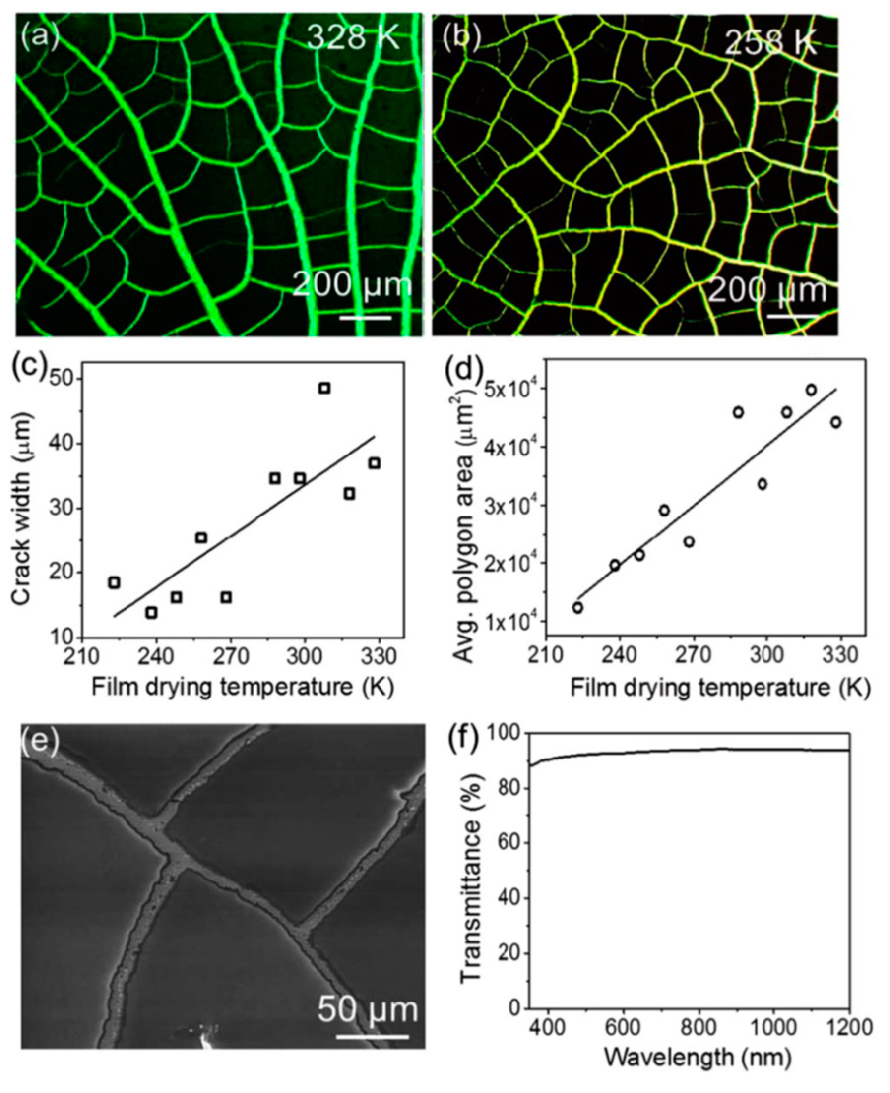
5.1. Drying Rate and Temperature
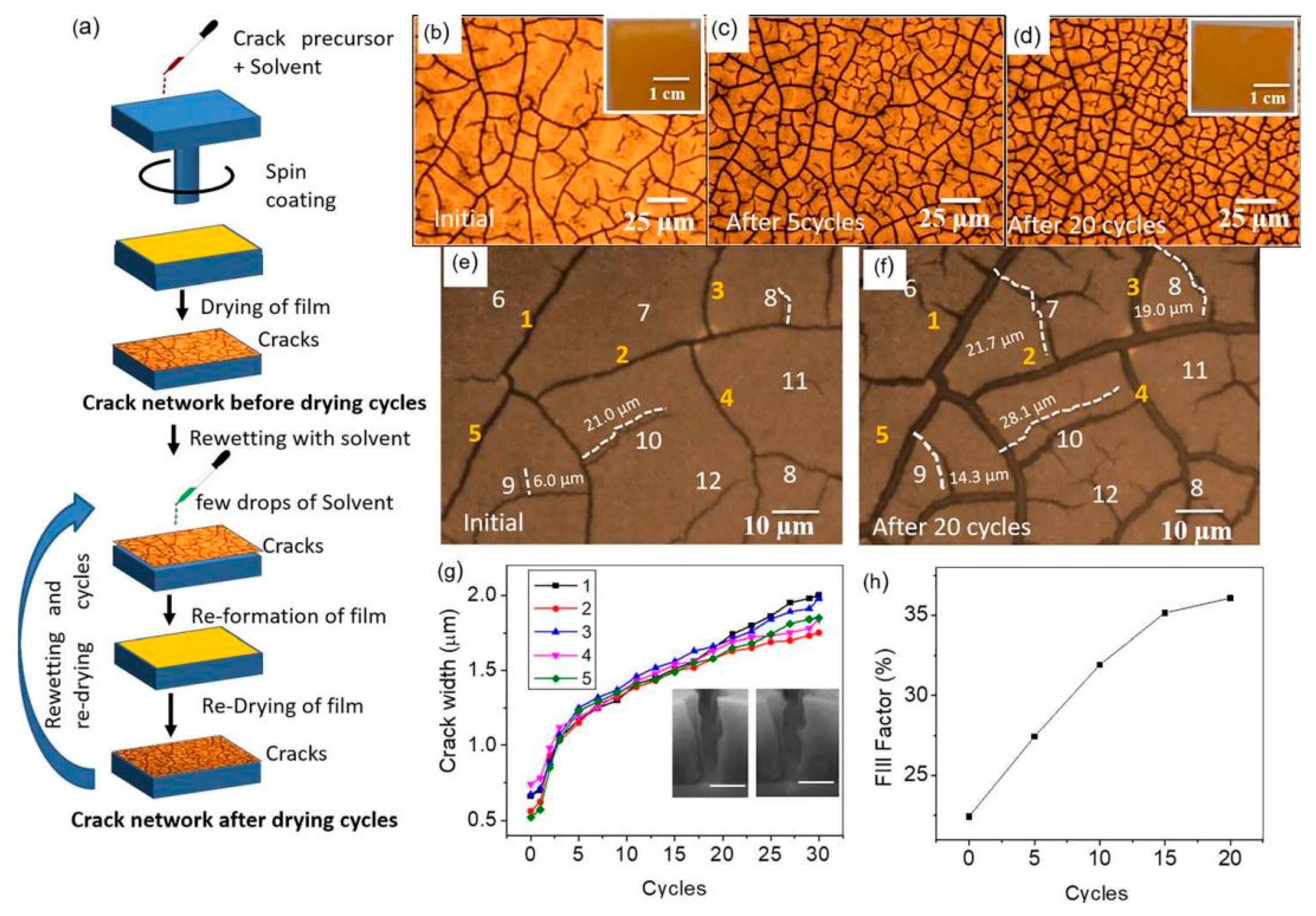
5.2. Wetting–Drying Cycles
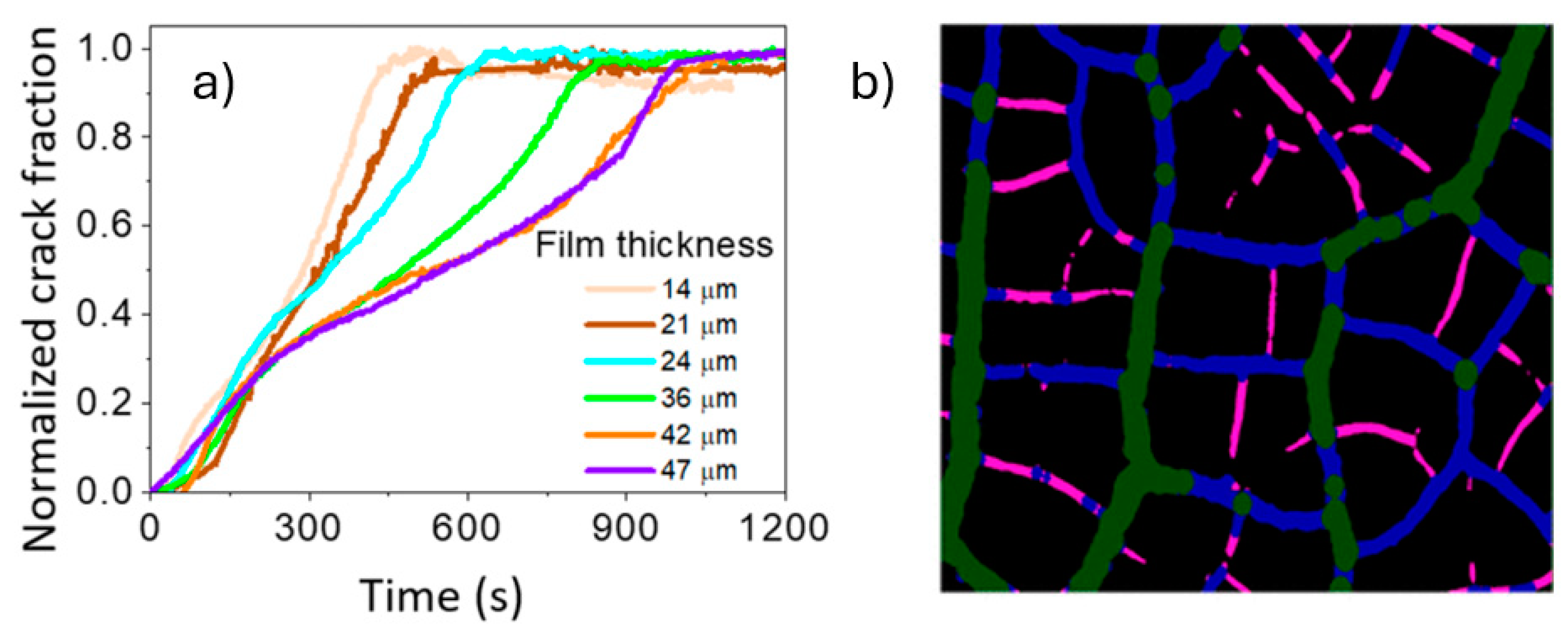
5.3. Layer Thickness
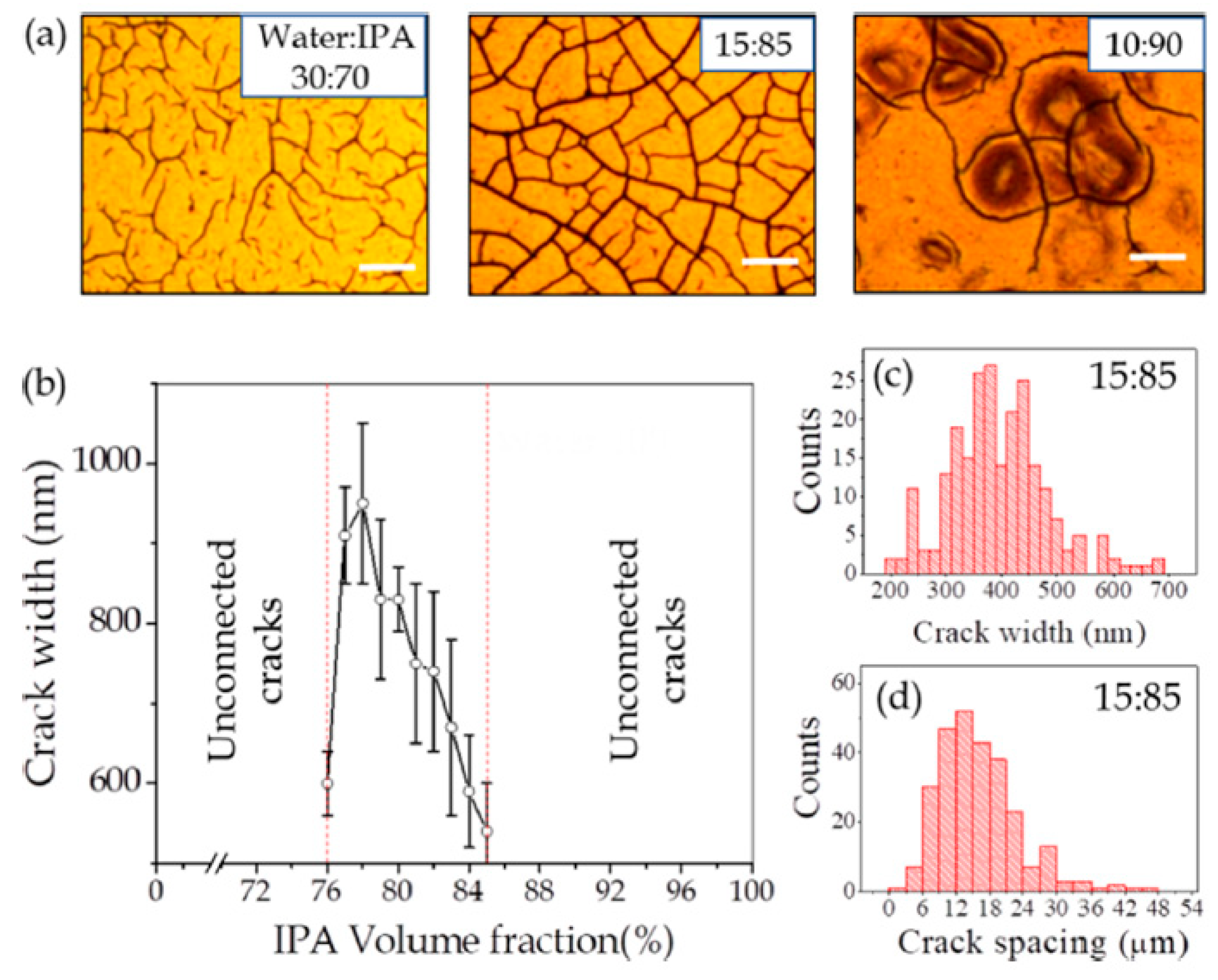
5.4. Solvents
5.5. Substrate Interactions and Surface Properties
6. Applications of Crack-Templated Patterns
6.1. Sustainability
6.2. Transparent Conductive Electrodes (TCEs)
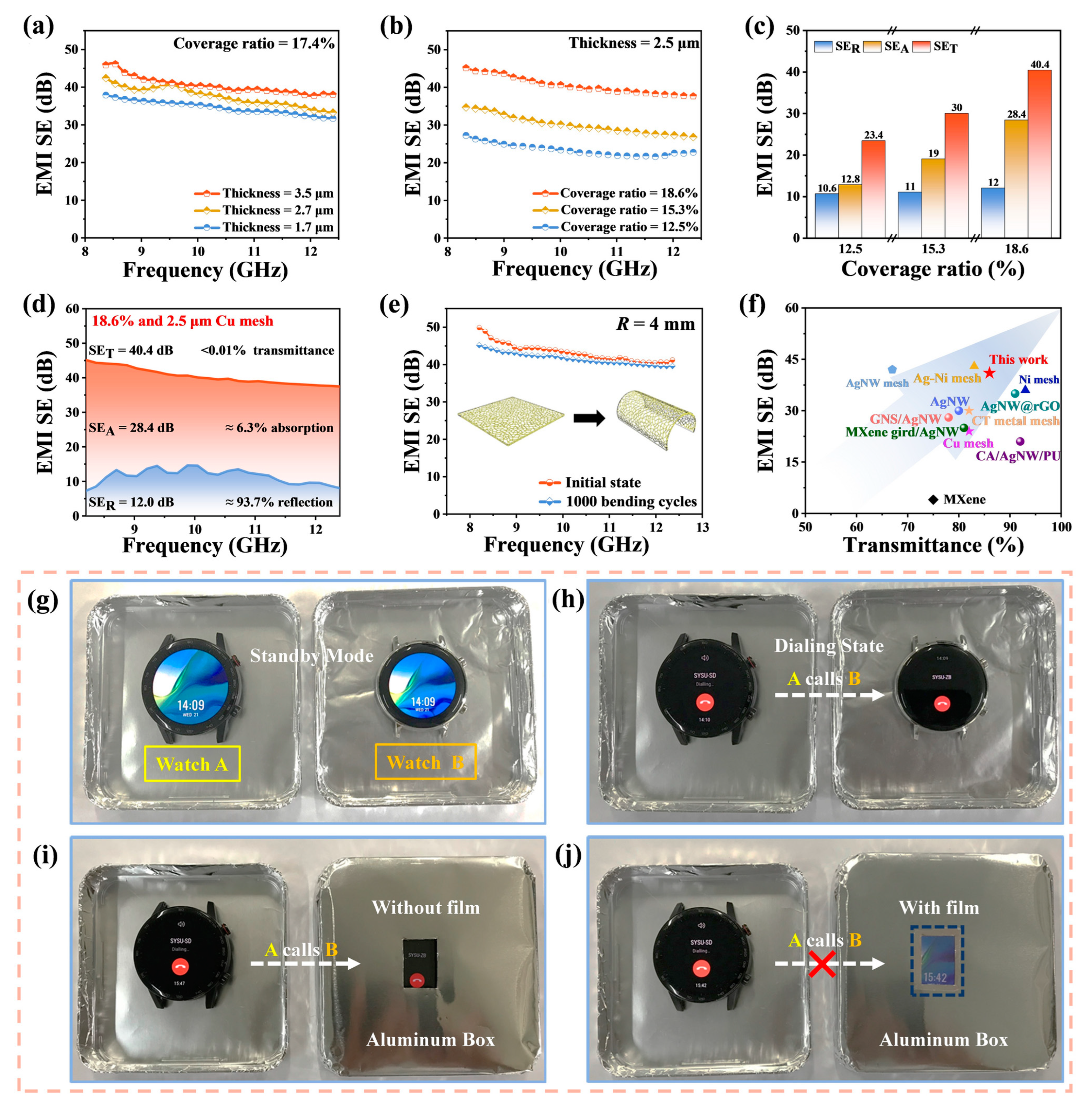
6.3. EMI-Shielding Devices
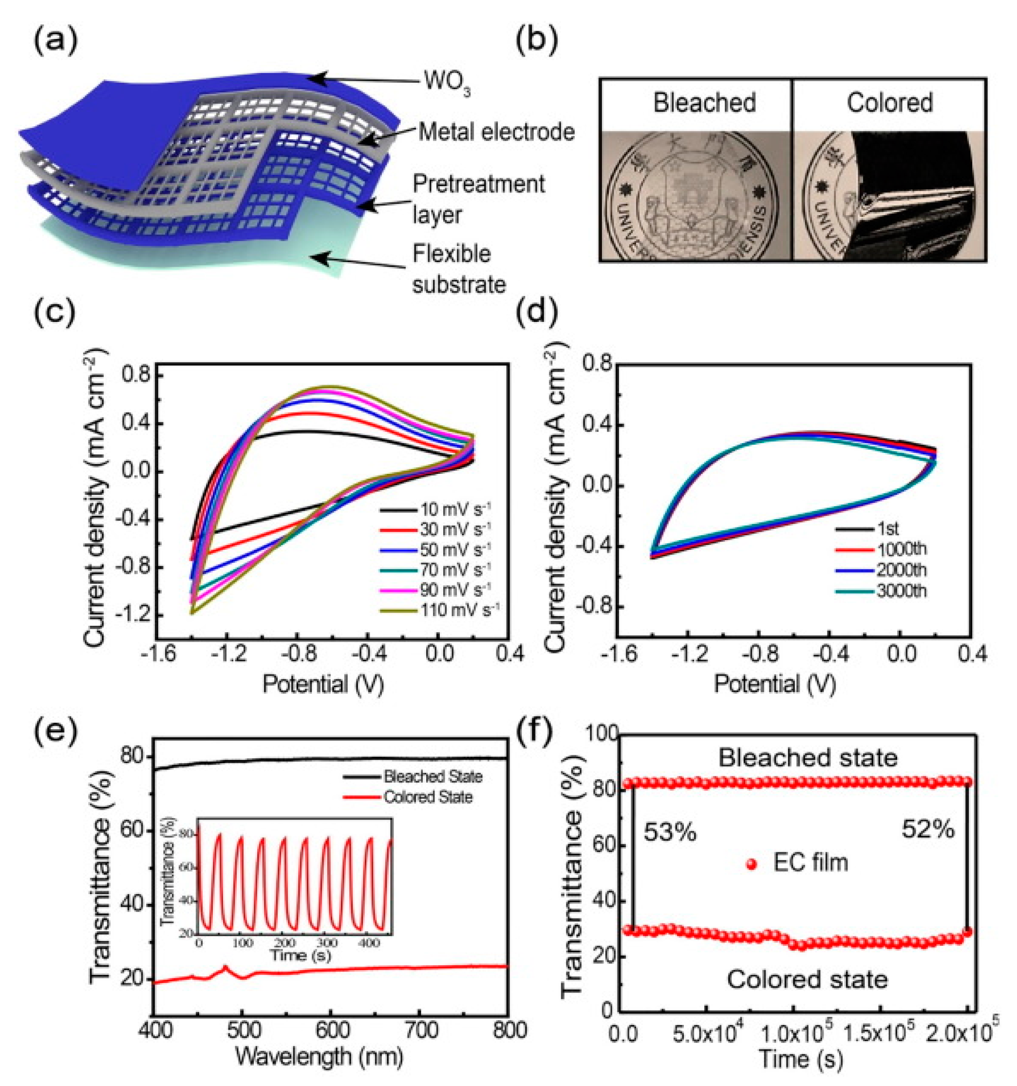
6.4. Smart Windows
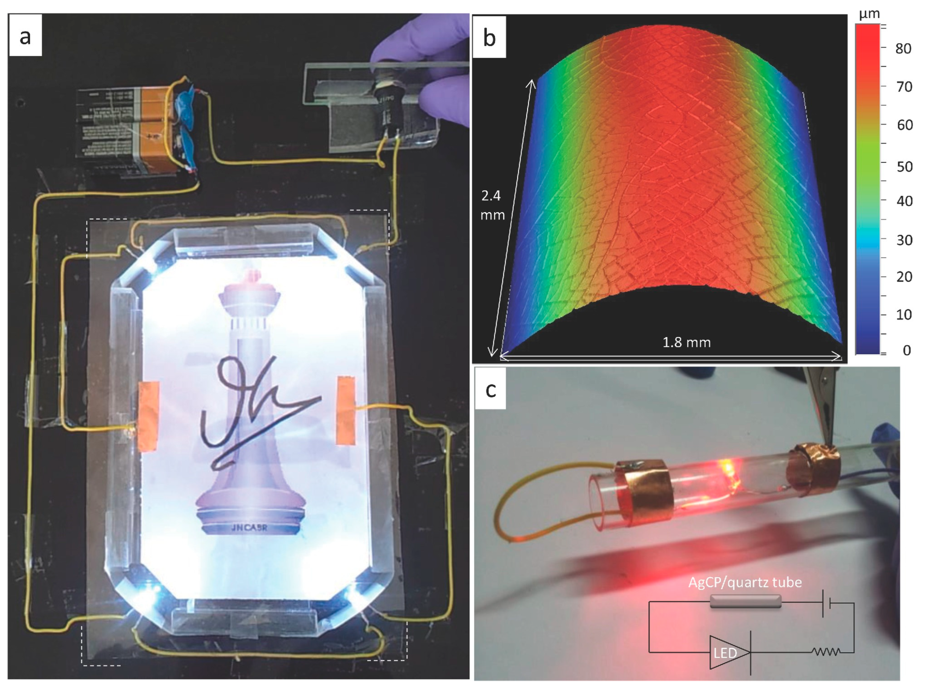
6.5. Transparent Heaters
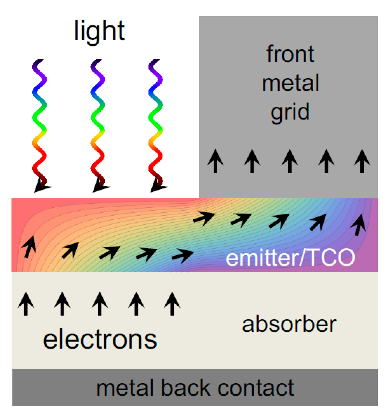
6.6. Solar Cells
6.7. Medical Devices
6.8. Other Applications
7. Conclusions and Future Directions
Author Contributions
Funding
Conflicts of Interest
References
- Gao, M.; Huang, X.; Zhao, Y. Formation of wavy-ring crack in drying droplet of protein solutions. Sci. China-Technol. Sci. 2018, 61, 949–958. [Google Scholar] [CrossRef]
- Adelung, R.; Aktas, O.; Franc, J.; Biswas, A.; Kunz, R.; Elbahri, M.; Kanzow, J.; Schürmann, U.; Faupel, F. Strain-controlled growth of nanowires within thin-film cracks. Nat. Mater. 2004, 3, 375–379. [Google Scholar] [CrossRef]
- Léang, M.; Giorgiutti-Dauphiné, F.; Lee, L.; Pauchard, L. Crack opening: From colloidal systems to paintings. Soft Matter 2017, 13, 5802–5808. [Google Scholar] [CrossRef]
- Flores, J. Mean-field crack networks on desiccated films and their applications: Girl with a Pearl Earring. Soft Matter 2017, 13, 1352–1356. [Google Scholar] [CrossRef] [PubMed]
- Laan, N.; Smith, F.; Nicloux, C.; Brutin, D. Morphology of drying blood pools. Forensic Sci. Int. 2016, 267, 104–109. [Google Scholar] [CrossRef] [PubMed]
- Prosser, J.; Brugarolas, T.; Lee, S.; Nolte, A.; Lee, D. Avoiding Cracks in Nanoparticle Films. Nano Lett. 2012, 12, 5287–5291. [Google Scholar] [CrossRef]
- Padovan, J.; Guo, Y. Moving Template Analysis of Crack-Growth—1. Procedure development. Eng. Fract. Mech. 1994, 48, 405–425. [Google Scholar] [CrossRef]
- Guo, Y.; Padovan, J. Moving Template Analysis of Crack-Growth—2. Multiple Crack Extension and Benchmarking. Eng. Fract. Mech. 1994, 48, 427–444. [Google Scholar] [CrossRef]
- Fan, H.; Werner, P.; Zacharias, M. Semiconductor nanowires: From self-organization to patterned growth. Small 2006, 2, 700–717. [Google Scholar] [CrossRef]
- Tomar, B.; Shahin, A.; Tirumkudulu, M. Cracking in drying films of polymer solutions. Soft Matter 2020, 16, 3476–3484. [Google Scholar] [CrossRef] [PubMed]
- Kim, N.; Cho, H.; Kim, Y.; Hwang, J.; Choi, J.; Yu, H. Formation of palladium nano-gap on self-cracked WO3 for hydrogen gas sensors. Int. J. Hydrogen Energy 2023, 48, 1234–1239. [Google Scholar] [CrossRef]
- Lim, M.; Kim, S.; Park, K.; Kim, Y.; Kim, J.; Ok, G.; Choi, S. Facile synthesis of self-aligned gold nanoparticles by crack templated reduction lithography. RSC Adv. 2017, 7, 13228–13231. [Google Scholar] [CrossRef]
- Yamamura, M. Adsorption-mediated nonlinearity of critical cracking thickness in drying nanoparticle-polymer suspensions. Aiche J. 2021, 67, e17229. [Google Scholar] [CrossRef]
- Kiruthika, S.; Rao, K.; Kumar, A.; Gupta, R.; Kulkarni, G. Metal wire network based transparent conducting electrodes fabricated using interconnected crackled layer as template. Mater. Res. Express 2014, 1, 026301. [Google Scholar] [CrossRef]
- Kappert, E.; Pavlenko, D.; Malzbender, J.; Nijmeijer, A.; Benes, N.; Tsai, P. Formation and prevention of fractures in sol-gel-derived thin films. Soft Matter 2015, 11, 882–888. [Google Scholar] [CrossRef]
- Piroird, K.; Lazarus, V.; Gauthier, G.; Lesaine, A.; Bonamy, D.; Rountree, C. Role of evaporation rate on the particle organization and crack patterns obtained by drying a colloidal layer. EPL 2016, 113, 38002. [Google Scholar] [CrossRef]
- Lama, H.; Basavaraj, M.; Satapathy, D. Desiccation cracks in dispersion of ellipsoids: Effect of aspect ratio and applied fields. Phys. Rev. Mater. 2018, 2, 085602. [Google Scholar] [CrossRef]
- Godard, P.; Guillot, A.; Zighem, F.; Thiaudière, D.; Faurie, D.; Renault, P. Strain ratio and thickness effects on plasticity and crack patterns of Nickel thin films. Scr. Mater. 2022, 213, 114638. [Google Scholar] [CrossRef]
- Ghosh, U.; Chakraborty, M.; Bhandari, A.; Chakraborty, S.; DasGupta, S. Effect of Surface Wettability on Crack Dynamics and Morphology of Colloidal Films. Langmuir 2015, 31, 6001–6010. [Google Scholar] [CrossRef] [PubMed]
- Tarasevich, Y.; Eserkepov, A.; Vodolazskaya, I. Electrical conductivity of crack-template-based transparent conductive films: A computational point of view. Phys. Rev. E 2023, 108, 044143. [Google Scholar] [CrossRef] [PubMed]
- Marthelot, J.; Roman, B.; Bico, J.; Teisseire, J.; Dalmas, D.; Melo, F. Self-Replicating Cracks: A Collaborative Fracture Mode in Thin Films. Phys. Rev. Lett. 2014, 113, 085502. [Google Scholar] [CrossRef]
- Kiruthika, S.; Gupta, R.; Rao, K.; Chakraborty, S.; Padmavathy, N.; Kulkarni, G. Large area solution processed transparent conducting electrode based on highly interconnected Cu wire network. J. Mater. Chem. C 2014, 2, 2089–2094. [Google Scholar] [CrossRef]
- Gupta, N.; Rao, K.; Srivastava, K.; Gupta, R.; Kumar, A.; Marconnet, A.; Fisher, T.; Kulkarni, G. Cosmetically Adaptable Transparent Strain Sensor for Sensitively Delineating Patterns in Small Movements of Vital Human Organs. ACS Appl. Mater. Interfaces 2018, 10, 44126–44133. [Google Scholar] [CrossRef] [PubMed]
- Gong, S.; Yap, L.; Zhu, B.; Zhai, Q.; Liu, Y.; Lyu, Q.; Wang, K.; Yang, M.; Ling, Y.; Lai, D.; et al. Local Crack-Programmed Gold Nanowire Electronic Skin Tattoos for In-Plane Multisensor Integration. Adv. Mater. 2019, 31, e1903789. [Google Scholar] [CrossRef]
- Li, T.; Li, S.; Li, X.; Xu, Z.; Zhao, J.; Shi, Y.; Wang, Y.; Yu, R.; Liu, X.; Xu, Q.; et al. A leaf vein-like hierarchical silver grids transparent electrode towards high-performance flexible electrochromic smart windows. Sci. Bull. 2020, 65, 225–232. [Google Scholar] [CrossRef]
- Kumar, A.; Pujar, R.; Gupta, N.; Tarafdar, S.; Kulkarni, G. Stress modulation in desiccating crack networks for producing effective templates for patterning metal network based transparent conductors. Appl. Phys. Lett. 2017, 111, 013502. [Google Scholar] [CrossRef]
- Rao, K.; Gupta, R.; Kulkarni, G. Fabrication of Large Area, High-Performance, Transparent Conducting Electrodes Using a Spontaneously Formed Crackle Network as Template. Adv. Mater. Interfaces 2014, 1, 1400090. [Google Scholar] [CrossRef]
- Ayatollahi, M.; Saboori, B. T-stress effects in mixed mode I/II/III brittle fracture. Eng. Fract. Mech. 2015, 144, 32–45. [Google Scholar] [CrossRef]
- Kim, M.; Kim, D.; Ha, D.; Kim, T. Cracking-assisted fabrication of nanoscale patterns for micro/nanotechnological applications. Nanoscale 2016, 8, 9461–9479. [Google Scholar] [CrossRef] [PubMed]
- Kozuka, H. Stress Evolution and Cracking in Sol–Gel- Derived Thin Films In Handbook of Sol-Gel Science and Technology; Springer International Publishing: Cham, Switzerland, 2018; pp. 275–311. [Google Scholar]
- Kumar, A.; Kulkarni, G. Time Evolution and Spatial Hierarchy of Crack Patterns. Langmuir 2021, 37, 13141–13147. [Google Scholar] [CrossRef] [PubMed]
- Chae, K.; Nguyen, V.; Lee, S.; Phung, T.; Sim, Y.; Seong, M.; Lee, S.; Ahn, Y.; Lee, S.; Ryu, S.; et al. Mechanical failures of Two-Dimensional materials on polymer substrates. Appl. Surf. Sci. 2022, 605, 154736. [Google Scholar] [CrossRef]
- Gong, L.; Xiang, L.; Zhang, J.; Chen, J.; Zeng, H. Fundamentals and Advances in the Adhesion of Polymer Surfaces and Thin Films. Langmuir 2019, 35, 15914–15936. [Google Scholar] [CrossRef] [PubMed]
- Liu, M.; Yu, S.; He, L.; Ni, Y. Recent progress on crack pattern formation in thin films. Soft Matter 2022, 18, 5906–5927. [Google Scholar] [CrossRef] [PubMed]
- Stylianou, R.; Velic, D.; Daves, W.; Ecker, W.; Stark, A.; Schell, N.; Tkadletz, M.; Schalk, N.; Czettl, C.; Mitterer, C. Stress relaxation through thermal crack formation in CVD TiCN coatings grown on WC-Co with different Co contents. Int. J. Refract. Met. Hard Mater. 2020, 86, 105102. [Google Scholar] [CrossRef]
- Mondal, S.; Agnihotri, S.; Faye, A. Theoretical solution for thermo-mechanical crack-tip stress field for transversely graded materials. J. Therm. Stress. 2022, 45, 101–116. [Google Scholar] [CrossRef]
- Baëtens, T.; Pallecchi, E.; Thomy, V.; Arscott, S. Cracking effects in squashable and stretchable thin metal films on PDMS for flexible microsystems and electronics. Sci. Rep. 2018, 8, 9492. [Google Scholar] [CrossRef]
- Guo, Z.; Li, C.; Zu, P.; Liu, Z.; Li, J.; Li, J. The kinetics of crack propagation in CVD graphene film. Diam. Relat. Mater. 2022, 126, 109056. [Google Scholar] [CrossRef]
- Mondal, I.; Kumar, A.; Rao, K.; Kulkarni, G. Parallel cracks from a desiccating colloidal layer under gravity flow and their use in fabricating metal micro-patterns. J. Phys. Chem. Solids 2018, 118, 232–237. [Google Scholar] [CrossRef]
- Li, J.; Li, L.; Wang, Z.; Li, C.; Wang, Q.; Wang, S. Controlled crack propagation of flexible Film/Substrate assembly by biaxial stress. Int. J. Solids Struct. 2022, 259, 112014. [Google Scholar] [CrossRef]
- Ma, X.; Lowensohn, J.; Burton, J. Universal scaling of polygonal desiccation crack patterns. Phys. Rev. E 2019, 99, 012802. [Google Scholar] [CrossRef]
- Kim, M.; Ha, D.; Kim, T. Cracking-assisted photolithography for mixed-scale patterning and nanofluidic applications. Nat. Commun. 2015, 6, 6247. [Google Scholar] [CrossRef] [PubMed]
- Dong, X.; Zhang, Y. An insight on egg white: From most common functional food to biomaterial application. J. Biomed. Mater. Res. Part B-Appl. Biomater. 2021, 109, 1045–1058. [Google Scholar] [CrossRef] [PubMed]
- Rehman, H.; Rehman, M.; Saqib, M.; Khan, S.; Khan, M.; Yang, Y.; Kim, S.; Rahman, S.; Kim, W. Highly Efficient and Wide Range Humidity Response of Biocompatible Egg White Thin Film. Nanomaterials 2021, 11, 1815. [Google Scholar] [CrossRef]
- Chandrabose, V.; Park, J.; Jung, S.; Wang, K.; Oh, J. Highly Porous Layered Double Hydroxide and Mixed Metal Oxide by Sacrificial Bio-Template, Egg White Foam. Crystals 2023, 13, 1603. [Google Scholar] [CrossRef]
- Li, Y.; Lv, T.; Zhao, F.; Zou, Y.; Lian, X.; Zhou, Q.; Liu, H.; An, D. Enhanced ethanol sensing and antibacterial activity of ZnO nanosheets synthesised using egg white as template. Mater. Technol. 2016, 31, 192–196. [Google Scholar] [CrossRef]
- Xiao, Z.; Zhong, W.; Ou, H.; Fu, H.; Xu, S.; Luo, Y. Photoelectric Properties of Transparent Conductive Metal Mesh Films Based on Crack Template and Its Application in Perovskite Solar Cells. In Proceedings of the Tenth International Conference on Thin Film Physics and Applications (TFPA 2019), Qingdao, China, 19–22 May 2019. [Google Scholar]
- Katekhong, W.; Charoenrein, S. Color and gelling properties of dried egg white: Effect of drying methods and storage conditions. Int. J. Food Prop. 2017, 20, 2157–2168. [Google Scholar] [CrossRef]
- Voronin, A.; Fadeev, Y.; Ivanchenko, F.; Dobrosmyslov, S.; Makeev, M.; Mikhalev, P.; Osipkov, A.; Damaratsky, I.; Ryzhenko, D.; Yurkov, G.; et al. Original concept of cracked template with controlled peeling of the cells perimeter for high performance transparent EMI shielding films. Surf. Interfaces 2023, 38, 102793. [Google Scholar] [CrossRef]
- Voronin, A.; Fadeev, Y.; Govorun, I.; Podshivalov, I.; Simunin, M.; Tambasov, I.; Karpova, D.; Smolyarova, T.; Lukyanenko, A.; Karacharov, A.; et al. Cu-Ag and Ni-Ag meshes based on cracked template as efficient transparent electromagnetic shielding coating with excellent mechanical performance. J. Mater. Sci. 2021, 56, 14741–14762. [Google Scholar] [CrossRef]
- Voronin, A.; Fadeev, Y.; Dobrosmyslov, S.; Simunin, M.; Khartov, S.; IOP. Random Ag mesh transparent heater obtained with a cracked template technique. In Proceedings of the II International Scientific Conference on Applied Physics, Information Technologies and Engineering 25, Krasnoyarsk, Russian, 25 September–4 October 2020. [Google Scholar]
- Peng, Q.; Li, S.; Han, B.; Rong, Q.; Lu, X.; Wang, Q.; Zeng, M.; Zhou, G.; Liu, J.; Kempa, K.; et al. Colossal Figure of Merit in Transparent-Conducting Metallic Ribbon Networks. Adv. Mater. Technol. 2016, 1, 1600095–1600099. [Google Scholar] [CrossRef]
- Pala, L.; Uday, V.; Gogoi, D.; Peela, N. Surface and photocatalytic properties of TiO2 thin films prepared by non-aqueous surfactant assisted sol-gel method. J. Environ. Chem. Eng. 2020, 8, 104267. [Google Scholar] [CrossRef]
- Muzzillo, C.; Reese, M.; Mansfield, L. Fundamentals of Using Cracked Film Lithography to Pattern Transparent Conductive Metal Grids for Photovoltaics. Langmuir 2020, 36, 4630–4636. [Google Scholar] [CrossRef] [PubMed]
- Ali, A.; Ismail, A.; Najmy, R.; Al-Hajry, A. Preparation and characterization of ZnO-SiO2 thin films as highly efficient photocatalyst. J. Photochem. Photobiol. A Chem. 2014, 275, 37–46. [Google Scholar] [CrossRef]
- Melnychenko, A.; Kudrawiec, R. Crack-Templated Wire-Like Semitransparent Electrodes with Unique Irregular Patterns. ACS Omega 2022, 7, 39181–39186. [Google Scholar] [CrossRef] [PubMed]
- Nandanwar, R.; Singh, P.; Haque, F. Effects of Non-Ionic Surfactants Poly(ethylene glycol) and Tritonx100 on the Preparation of SiO2 Nanoparticles by Sol-Gel Process. J. Adv. Phys. 2014, 3, 141–145. [Google Scholar] [CrossRef]
- Gupta, R.; Rao, K.; Srivastava, K.; Kumar, A.; Kiruthika, S.; Kulkarni, G. Spray Coating of Crack Templates for the Fabrication of Transparent Conductors and Heaters on Flat and Curved Surfaces. ACS Appl. Mater. Interfaces 2014, 6, 13688–13696. [Google Scholar] [CrossRef]
- Koga, S.; Inasawa, S. Packing structures and formation of cracks in particulate films obtained by drying colloid-polymer suspensions. Colloids Surf. A Physicochem. Eng. Asp. 2019, 563, 95–101. [Google Scholar] [CrossRef]
- Arasan, S.; Aktas, M.; Balcioglu, H. Fracture toughness of woven glass and carbon reinforced hybrid and non-hybrid composite plates. Polym. Compos. 2018, 39, 783–793. [Google Scholar] [CrossRef]
- Truong, H.; Martinez, M.; Ochoa, O.; Lagoudas, D. Mode I fracture toughness of hybrid co-cured Al-CFRP and NiTi-CFRP interfaces: An experimental and computational study. Compos. Part A Appl. Sci. Manuf. 2020, 135, 105925. [Google Scholar] [CrossRef]
- Ayyagari, S.; Al-Haik, M. Mitigating Crack Propagation in Hybrid Composites: An Experimental and Computational Study. J. Compos. Sci. 2024, 8, 122. [Google Scholar] [CrossRef]
- Tomar, B.; Tirumkudulu, M. Critical cracking thickness of drying polymer films. Soft Matter 2023, 19, 3910–3916. [Google Scholar] [CrossRef]
- Lama, H.; Basavaraj, M.; Satapathy, D. Tailoring crack morphology in coffee-ring deposits via substrate heating. Soft Matter 2017, 13, 5445–5452. [Google Scholar] [CrossRef]
- Yoon, J.; Phuong, N.; Kim, J.; Choi, D.; Whang, K.; Yoo, Y. Wetting characteristics of the anodic aluminum oxide template and fabrication of cracks using ultraviolet curable resin solution. Appl. Phys. Lett. 2014, 104, 091603. [Google Scholar] [CrossRef]
- Thorimbert, F.; Brachfeld, A.; Odziomek, M.; Boissiere, C.; Amenitsch, H.; Naumenko, D.; Mattana, G.; Baccile, N.; Faustini, M. Microfabrication through Self-Ordering of Cracks: Mechanism, Upscaling and Application for Transparent Electrodes. Adv. Mater. Technol. 2024, 9, 2400353. [Google Scholar] [CrossRef]
- Hennessy, M.; Ferretti, G.; Cabral, J.; Matar, O. A minimal model for solvent evaporation and absorption in thin films. J. Colloid Interface Sci. 2017, 488, 61–71. [Google Scholar] [CrossRef] [PubMed]
- Lilin, P.; Ibrahim, M.; Bischofberger, I. Crack densification in drying colloidal suspensions. Sci. Adv. 2024, 10, eadp3746. [Google Scholar] [CrossRef] [PubMed]
- Rheinschmidt, F.; Felger, J.; Rosendahl, P. A closed-form analytical variational approach to thermally induced thin-film delamination. Proc. Inst. Mech. Eng. Part C J. Mech. Eng. Sci. 2024, 238, 7231–7240. [Google Scholar] [CrossRef]
- Skvortsov, A.; Koryachko, M.; Skvortsov, P.; Luk’yanov, M. On the Issue of Crack Formation in a Thin Dielectric Layer on Silicon under Thermal Shock. J. Mater. Eng. Perform. 2020, 29, 4390–4395. [Google Scholar] [CrossRef]
- Li, X.; Shan, Y.; Xia, F.; Chen, C.; Lu, S.; Hu, X. Preparation of Diamond Films with Cracked Textures on Stainless Steel Using W/W-N Film as an Interlayer. Coatings 2024, 14, 1494. [Google Scholar] [CrossRef]
- Li, Y.; Lv, C.; Li, Z.; Quéré, D.; Zheng, Q. From coffee rings to coffee eyes. Soft Matter 2015, 11, 4669–4673. [Google Scholar] [CrossRef] [PubMed]
- Shi, P.; Wang, W.; Liu, D.; Zhang, J.; Ren, W.; Tian, B.; Zhang, J. Structural and Electrical Properties of Flexible ITO/In2O3 Thermocouples on PI Substrates under Tensile Stretching. ACS Appl. Electron. Mater. 2019, 1, 1105–1111. [Google Scholar] [CrossRef]
- Gong, S.; Yap, L.; Zhu, Y.; Zhu, B.; Wang, Y.; Ling, Y.; Zhao, Y.; An, T.; Lu, Y.; Cheng, W. A Soft Resistive Acoustic Sensor Based on Suspended Standing Nanowire Membranes with Point Crack Design. Adv. Funct. Mater. 2020, 30, 1910717. [Google Scholar] [CrossRef]
- Bird, D.; Caravaca, E.; Laquidara, J.; Luhmann, K.; Ravindra, N.; Minerals, M.M.S. Formulation of Curable Resins Utilized in Stereolithography. In Proceedings of the TMS 2019 148TH Annual Meeting & Exhibition Supplemental Proceedings, San Antonio, TX, USA, 10–14 March 2019; pp. 1575–1587. [Google Scholar]
- Johansson, E.; Lidström, O.; Johansson, J.; Lyckfeldt, O.; Adolfsson, E. Influence of Resin Composition on the Defect Formation in Alumina Manufactured by Stereolithography. Materials 2017, 10, 138. [Google Scholar] [CrossRef]
- Tian, Q.; Yu, D. Preparation and properties of polymer microspheres filled epoxy composite films by UV-curable polymerization. Mater. Des. 2016, 107, 221–229. [Google Scholar] [CrossRef]
- McIlroy, D.; Pauchard, L. Evolution of the crack patterns in nanostructured films with subsequent wetting and drying cycles. EPL 2024, 147, 56002. [Google Scholar] [CrossRef]
- Husain, S.; Kreiml, P.; Trost, C.; Faurie, D.; Cordill, M.; Renault, P. Residual stress and thickness effects on fracture behavior of trilayer films during uniaxial loading. Thin Solid Film. 2024, 788, 140173. [Google Scholar] [CrossRef]
- Abdel-Mohti, A.; Garbash, A.; Almagahwi, S.; Shen, H. Effect of Layer and Film Thickness and Temperature on the Mechanical Property of Micro- and Nano-Layered PC/PMMA Films Subjected to Thermal Aging. Materials 2015, 8, 2062–2075. [Google Scholar] [CrossRef]
- Coleman, K.; Bermejo, R.; Leguillon, D.; Trolier-McKinstry, S. Thickness Dependence of crack initiation and propagation in stacks for piezoelectric microelectromechanical systems. Acta Mater. 2020, 191, 245–252. [Google Scholar] [CrossRef]
- Alkhazali, A.; Hamasha, S.; Hamasha, M.; Khaled, H.; Massadeh, R. Crack Development and Electrical Degradation in Chromium Thin Films Under Tensile Stress on PET Substrates. Coatings 2024, 14, 1403. [Google Scholar] [CrossRef]
- Pujar, R.; Kumar, A.; Rao, K.; Sadhukhan, S.; Dutta, T.; Tarafdar, S.; Kulkarni, G. Narrowing Desiccating Crack Patterns by an Azeotropic Solvent for the Fabrication of Nanomesh Electrodes. Langmuir 2019, 35, 16130–16135. [Google Scholar] [CrossRef] [PubMed]
- DeCarlo, K.; Shokri, N. Effects of substrate on cracking patterns and dynamics in desiccating clay layers. Water Resour. Res. 2014, 50, 3039–3051. [Google Scholar] [CrossRef]
- Kumar, S.; Basavaraj, M.; Satapathy, D. Effect of Colloidal Surface Charge on Desiccation Cracks. Langmuir 2023, 39, 10249–10258. [Google Scholar] [CrossRef] [PubMed]
- Kumar, S.; Basavaraj, M.; Satapathy, D. Effect of the Shape of the Confining Boundary and Particle Shape Anisotropy on the Morphology of Desiccation Cracks. Langmuir 2022, 38, 7906–7913. [Google Scholar] [CrossRef] [PubMed]
- Haghshenas, A.; Khonsari, M. Damage accumulation and crack initiation detection based on the evolution of surface roughness parameters. Int. J. Fatigue 2018, 107, 130–144. [Google Scholar] [CrossRef]
- Li, Q.; Weinell, C.; Kiil, S. Detection and Quantification of Premature Crack Formation in Curing Epoxy Coatings. Ind. Eng. Chem. Res. 2022, 61, 13092–13103. [Google Scholar] [CrossRef]
- Bhattacharjee, S.; Srivastava, S. Ordered stripes to crack patterns in dried particulates of DNA-coated gold colloids via modulating nanoparticle-substrate interactions. Soft Matter 2023, 19, 2265–2274. [Google Scholar] [CrossRef] [PubMed]
- Kim, H.; Abdelrahman, M.; Choi, J.; Kim, H.; Maeng, J.; Wang, S.; Javed, M.; Rivera-Tarazona, L.; Lee, H.; Ko, S.; et al. From Chaos to Control: Programmable Crack Patterning with Molecular Order in Polymer Substrates. Adv. Mater. 2021, 33, 2008434. [Google Scholar] [CrossRef]
- Chen, Z.; Yang, S.; Huang, J.; Gu, Y.; Huang, W.; Liu, S.; Lin, Z.; Zeng, Z.; Hu, Y.; Chen, Z.; et al. Flexible, Transparent and Conductive Metal Mesh Films with Ultra-High FoM for Stretchable Heating and Electromagnetic Interference Shielding. Nano-Micro Lett. 2024, 16, 92. [Google Scholar] [CrossRef] [PubMed]
- Mondal, I.; Ganesh, M.K.; Rao, K.D.M.; Kulkarni, G.U. Lithography-Free, Wafer-Scale, Solution-Based Fabrication of Network of Microchannels: A Template Towards Cost-Effective Microfluidic Devices and Optoelectronics. 2024. Available online: https://ssrn.com/abstract=4841423 (accessed on 15 November 2024).
- Yan, J.; Wang, Z.; Bai, W.; Wang, C.; Jiang, Y.; Shi, X.; Chen, Y.; Liu, J.; Gao, J. Kill Two Birds with One Stone: Cracking Lithography Technology for High-Performance Flexible Metallic Network Transparent Conductors and Metallic Micronano Sheets. ACS Appl. Mater. Interfaces 2024, 16, 59637–59647. [Google Scholar] [CrossRef] [PubMed]
- Zarei, M.; Li, M.; Medvedeva, E.; Sharma, S.; Kim, J.; Shao, Z.; Walker, S.; Lemieux, M.; Liu, Q.; Leu, P. Flexible Embedded Metal Meshes by Sputter-Free Crack Lithography for Transparent Electrodes and Electromagnetic Interference Shielding. ACS Appl. Mater. Interfaces 2024, 16, 6382–6393. [Google Scholar] [CrossRef]
- Haque, S.; Haque, R.; Dutta, T. pH regulated desiccation crack network: A versatile template for Transparent Conducting Sheet fabrication. Phys. Scr. 2023, 98, 085942. [Google Scholar] [CrossRef]
- Mondal, I.; Ganesha, M.; Singh, A.; Kulkarni, G. Affordable Smart Windows with Dual-Functionality: Electrochromic Color Switching and Charge Storage. Adv. Mater. Technol. 2023, 8, 2300651. [Google Scholar] [CrossRef]
- Muzzillo, C.; Reese, M.; Lee, C.; Xiong, G. Cracked Film Lithography with CuGaOx Buffers for Bifacial CdTe Photovoltaics. Small 2023, 19, 2301939. [Google Scholar] [CrossRef] [PubMed]
- Mondal, I.; Kiruthika, S.; Ganesha, M.; Baral, M.; Kumar, A.; Vimala, S.; Madhuri, P.; Nair, G.; Prasad, S.; Singh, A.; et al. ITO-free large area PDLC smart windows: A cost-effective fabrication using spray coated SnO2 on an invisible Al mesh. J. Mater. Chem. A 2021, 9, 23157–23168. [Google Scholar] [CrossRef]
- Mondal, I.; Bahuguna, G.; Ganesha, M.; Verma, M.; Gupta, R.; Singh, A.; Kulkarni, G. Scalable Fabrication of Scratch-Proof Transparent Al/F-SnO2 Hybrid Electrodes with Unusual Thermal and Environmental Stability. ACS Appl. Mater. Interfaces 2020, 12, 54203–54211. [Google Scholar] [CrossRef]
- Walia, S.; Singh, A.; Rao, V.; Bose, S.; Kulkarni, G. Metal mesh-based transparent electrodes as high-performance EMI shields. Bull. Mater. Sci. 2020, 43, 187. [Google Scholar] [CrossRef]
- Dong, G.; Liu, S.; Pan, M.; Zhou, G.; Liu, J.; Kempa, K.; Gao, J. Bioinspired High-Adhesion Metallic Networks as Flexible Transparent Conductors. Adv. Mater. Technol. 2019, 4, 1900056. [Google Scholar] [CrossRef]
- Urgunde, A.; Kumar, A.; Shejale, K.; Sharma, R.; Gupta, R. Metal Wire Networks Functionalized with Nickel Alkanethiolate for Transparent and Enzymeless Glucose Sensors. ACS Appl. Nano Mater. 2018, 1, 5571–5580. [Google Scholar] [CrossRef]
- Yang, C.; Merlo, J.; Kong, J.; Xian, Z.; Han, B.; Zhou, G.; Gao, J.; Burns, M.; Kempa, K.; Naughton, M. All-Solution-Processed, Scalable, Self-Cracking Ag Network Transparent Conductor. Phys. Status Solidi A Appl. Mater. Sci. 2018, 215, 1700504. [Google Scholar] [CrossRef]
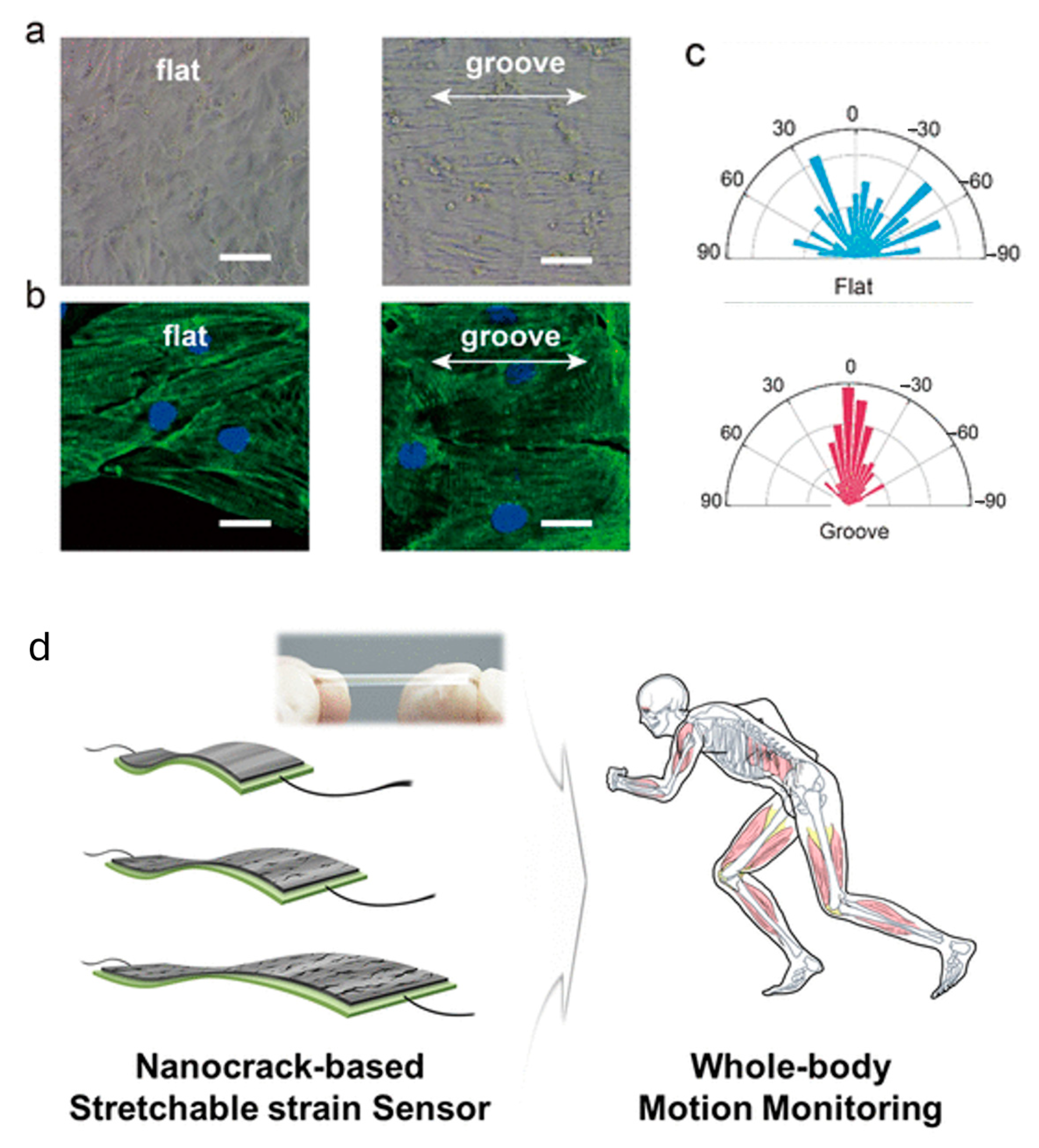
- Jeon, H.; Hong, S.; Kim, M.; Cho, S.; Lim, G. Omni-Purpose Stretchable Strain Sensor Based on a Highly Dense Nanocracking Structure for Whole-Body Motion Monitoring. ACS Appl. Mater. Interfaces 2017, 9, 41712–41721. [Google Scholar] [CrossRef]
- Suh, Y.; Hong, S.; Lee, J.; Lee, H.; Jung, S.; Kwon, J.; Moon, H.; Won, P.; Shin, J.; Yeo, J.; et al. Random nanocrack, assisted metal nanowire-bundled network fabrication for a highly flexible and transparent conductor. RSC Adv. 2016, 6, S7434–S7440. [Google Scholar] [CrossRef]
- Kim, Y.; Tak, Y.; Kim, H.; Kim, W.; Yoo, H.; Kim, H. Facile fabrication of wire-type indium gallium zinc oxide thin-film transistors applicable to ultrasensitive flexible sensors. Sci. Rep. 2018, 8, 5546. [Google Scholar] [CrossRef] [PubMed]
- Li, P.; Zhao, Y.; Ma, J.; Yang, Y.; Xu, H.; Liu, Y. Facile Fabrication of Ultraflexible Transparent Electrodes Using Embedded Copper Networks for Wearable Pressure Sensors. Adv. Mater. Technol. 2020, 5, 1900823. [Google Scholar] [CrossRef]
- Gupta, R.; Kumar, A.; Sadasivam, S.; Walia, S.; Kulkarni, G.; Fisher, T.; Marconnet, A. Microscopic Evaluation of Electrical and Thermal Conduction in Random Metal Wire Networks. ACS Appl. Mater. Interfaces 2017, 9, 13703–13712. [Google Scholar] [CrossRef]
- Carulli, F.; Scavia, G.; Lassi, E.; Pasini, M.; Galeotti, F.; Brovelli, S.; Giovanella, U.; Luzzati, S. A bifunctional conjugated polyelectrolyte for the interfacial engineering of polymer solar cells. J. Colloid Interface Sci. 2019, 538, 611–619. [Google Scholar] [CrossRef]
- Cui, Y.; Hong, L.; Hou, J. Organic Photovoltaic Cells for Indoor Applications: Opportunities and Challenges. ACS Appl. Mater. Interfaces 2020, 12, 38815–38828. [Google Scholar] [CrossRef] [PubMed]
- Meng, R.; Jiang, Q.; Liu, D. Balancing efficiency and transparency in organic transparent photovoltaics. NPJ Flex. Electron. 2022, 6, 39. [Google Scholar] [CrossRef]
- Park, B.; Lee, S.; Choi, H.; Kim, J.; Hong, H.; Jeong, C.; Kang, D.; Kim, T. A semi-permanent and durable nanoscale-crack-based sensor by on-demand healing. Nanoscale 2018, 10, 4354–4360. [Google Scholar] [CrossRef]
- Wang, L.; Xu, X.; Chen, J.; Su, W.; Zhang, F.; Li, A.; Li, C.; Xu, C.; Sun, Y. Crack Sensing of Cardiomyocyte Contractility with High Sensitivity and Stability. ACS Nano 2022, 16, 12645–12655. [Google Scholar] [CrossRef] [PubMed]
- Attri, R.; Mondal, I.; Yadav, B.; Kulkarni, G.; Rao, C. Neuromorphic devices realised using self-forming hierarchical Al and Ag nanostructures: Towards energy-efficient and wide ranging synaptic plasticity. Mater. Horiz. 2024, 11, 737–746. [Google Scholar] [CrossRef]
- Evrova, O.; Hosseini, V.; Milleret, V.; Palazzolo, G.; Zenobi-Wong, M.; Sulser, T.; Buschmann, J.; Eberli, D. Hybrid Randomly Electrospun Poly(lactic-co-glycolic acid):Poly(ethylene oxide) (PLGA:PEO) Fibrous Scaffolds Enhancing Myoblast Differentiation and Alignment. ACS Appl. Mater. Interfaces 2016, 8, 31574–31586. [Google Scholar] [CrossRef] [PubMed]


| Aspect of Crack Formation | Details |
|---|---|
| Stresses | Intrinsic: Stresses originating from the material’s internal structure (e.g., due to phase changes, thermal expansion, or material defects). |
| Residual: Stresses remaining in a material after processing or deformation (e.g., due to cooling, phase transformations, or manufacturing processes). | |
| Contributors/defects | Grain boundaries: Cracks can form or propagate along grain boundaries, which are weak points in crystalline materials. |
| Voids: Internal voids or pores within the material that can lead to crack formation under stress. | |
| Surface irregularities: Surface roughness or defects, including scratches or inclusions, that can act as crack initiation sites. | |
| Adhesion to the substrate: Poor adhesion between layers or to the substrate can lead to delamination or crack initiation. | |
| Orientation | Random: Cracks propagate in random directions based on stress distribution and material properties. |
| Unidirectional: Cracks propagate in a single direction, typically in response to directional stresses (e.g., along the length of a material). | |
| Bi/Multidirectional: Cracks propagate in multiple directions, often influenced by complex loading or multi-axial stress conditions. |
| Parameter | Materials | Effect on Crack Formation | References |
|---|---|---|---|
| Drying Temperature |
| Higher temperatures: ordered, aligned cracks due to Marangoni flow. Lower temperatures: irregular, finer cracks due to capillary-driven flow. | [14,64] |
| Drying Rate |
| Faster drying: smaller fragments, near-crystalline structures. Slower drying: larger fragments, amorphous structures, reduced crack propagation. | [16] |
| Wetting–drying cycles |
| Non-connected crack networks evolve and stabilize over cycles, exhibiting a shielding effect. Growth through existing cracks and nucleation of new cracks. Crack length increases in a staircase pattern over cycles. | [78] |
| Layer thickness |
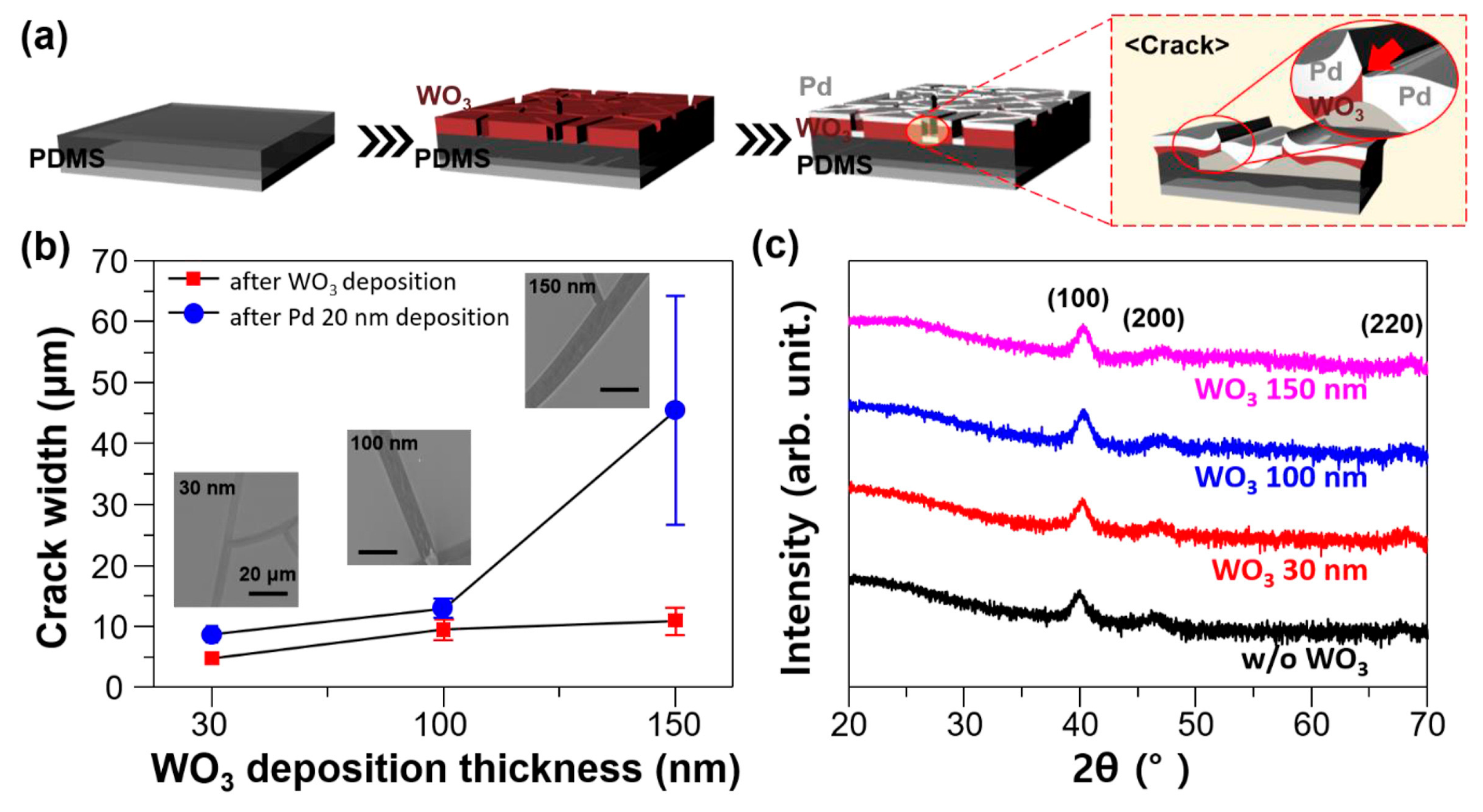
| Thicker middle layers and higher compressive stress in top layers: higher critical strain for crack initiation, lower crack density. | [79] |
| Thinner layers (~30 nm): improved stiffness and strength during thermal aging. | [80] | |
| Thinner films exhibit higher strength and Weibull modulus. | [81] | |
| Thinner films (20–100 nm): higher strength in equibiaxial strain tests (EBST) vs. uniaxial tests (UST). Thicker films (600 nm): similar strength in EBST and UST. Straighter cracks in thinner films; sinuous cracks in thicker films. | [18] | |
| Crack width and spacing grow linearly with layer thickness, critical threshold at ~700 nm for interconnected patterns. | [27] | |
| Thinner films (100 nm): early, widespread, and branched cracks even at low strain. Thicker films (200 nm): delayed crack initiation, fewer but deeper and more linear cracks. | [82] | |
| Solvents |
| Addition of ethyl acetate to ethanolic suspensions promotes uniform crack patterns. | [14,22] |
| Water + IPA mixtures enhance crack uniformity. | [83] | |
| Addition of DMSO to prepolymer enhances crack generation via volume shrinkage during curing. | [65] | |
| Substrate Wettability |
| Hydrophobic substrates show slower crack propagation and higher stress resistance compared to hydrophilic substrates. | [19] |
| Particle Size |
| Larger particles reduce crack density but increase crack width and length. | [84] |
| Surface Charge of Colloids |
| Positively charged colloids: wider spacing and faster growth. Negatively charged colloids: narrower spacing, slower growth. | [85] |
| Substrate Hardness |
| Softer substrates: lower critical thickness, more cracking is produced. Harder substrates: films remain crack-free. | [10] |
| Particle Shape Anisotropy |
| Isotropic particles: radial cracks. Anisotropic particles: azimuthal (circular) cracks due to alignment of ellipsoids’ major axis with contact line. | [86] |
| Crack Template Material | Mesh Material | Thicknesses | Transmittance | Resistance | Applications | Ref. |
|---|---|---|---|---|---|---|
| Acrylic emulsion | Cu | 1.7–3.5 μm (Cu mesh) | 85.8% (550 nm) | 0.18–0.53 Ω/sq | EMI shielding and EM-compatible optoelectronic devices | [91] |
| Crackle precursor | Au–Cu | 5 nm (Au) 650 nm (Cu) ~10 μm (crack width) | ~88% | ~5 Ω/sq | Microfluidic devices, capillary cooling systems, optoelectronics | [92] |
| Egg white | Ag | ~130 μm (cracks) 3–10 μm (Ag network) 15 μm (Ag-Re micro-nanosheets) | ~88.1% | ~9 Ω/sq | Flexible display technologies, lighting, sensing | [93] |
| Acrylic emulsion (CA-600) | Ag | ~1.8 μm (Ag) <5 μm widths, 5 μm depths (cracks) | 91%–93% | 0.54–1.4 Ω/sq | Transparent electrodes and EMI shielding | [94] |
| Silicate synthetic clay (Laponite), pH values: 7.8–12.7 | Graphite | Few μm | Peak: ~80% (540 nm); | 10–50 kΩ | Solar cells, touch screens, transparent heaters | [95] |
| Low-cost crackle precursor | Al_SnO2_WO3 | 530 nm (WO3) | Filters at 400 nm (pH 8.7, 12.2, 12.5); transparent all λ at other pH values: ~88% (decreasing with applied voltage) | 5 Ω/sq | Smart windows | [96] |
| PMMA (30% wt) on CdTe/CuGaOx | Au | 50 nm (Au) 3 nm (CuGaOx) 2 μm (wire width) | ~77% | 8.3 Ω/sq | Photovoltaics | [97] |
| Egg white | Ag | 2.5 μm (Ag) 4 nm (PMMA spacer in sandwich structure) | ~89% | 0.28–1.59 Ω/sq | EMI shielding | [49] |
| ZnO + PVP on quartz, sapphire or glass | Ag | 200 nm (Ag) 6 μm (crack layer) | ~83% (550 nm) (quartz > sapphire and glass) | Quartz = 13.55 Ω/sq; sapphire = 10.45 Ω/sq; glass = 13.65 Ω/sq | Encryption, solar cells, touch panels, light-emitting diodes, transparent heaters | [56] |
| Acrylic resin | Al-SnO2 | <30 μm | 85% (Al-SnO2) 92% (Al) | 5 Ω/sq | Smart windows | [98] |
| Egg white | Cu-Ag, Ni-Ag | 1.92 μm (Cu) 0.95 μm (Ni) 200 nm (Ag) | 82%–88% (Cu-Ag) 78%–87% (Ni-Ag) (550 nm) | 0.06–1.52 Ω/sq (Cu-Ag); 0.7–9.3 Ω/sq (Ni-Ag) | EMI shielding | [50] |
| TiO2 | WO3/Ag | 30 nm (WO3) 3–10 μm (crack width) | 81% | 1.36 Ω/sq | Smart windows | [25] |
| Crackle precursor | Al-SnO2 | ~400 nm (Al) ~200 nm (SnO2) | ~83% (550 nm) | 5.5 Ω/sq | Optoelectronics and photovoltaics | [99] |
| TiO2, PMMA, or PS | Cu | 3–45 μm (PS and PMMA); 25–140 μm (TiO2); Cu = 1/3 of template thickness | 80%–90% (TiO2) >90% (PS and PMMA) (450–890 nm) | ≥100 Ω/sq | Photovoltaics | [54] |
| Egg white | Ag | 200–600 nm (Ag) | 84%–91% (550 nm) | 1.6–21 Ω/sq | Transparent heaters (e.g., anti-fogging and anti-icing coatings) | [51] |
| Acrylic emulsion | Cu | 1 μm (Cu) | ~85% | 0.83 Ω/sq | EMI shielding, Joule heater | [100] |
| Nail polish + polyimide (PI) | Ag | 100–400 nm (Ag) | ~85% | 1.5 Ω/sq | Photovoltaics | [101] |
| Sputtered Au under tensile stretching | Au | 120 nm (Au) | n. a. | ~205 Ω (V-AuNWs/PDMS thin film) ~7100–7300 Ω (V-AuNWs-based sensor) | Wearable electronic tattoos (e.g., glucose and lactate sensors) | [24] |
| Acrylic resin | Cu | 80 nm (Cu) ~400 nm (crack width) ~15 μm (crack spacing) | ~87.5% | 10 Ω/sq | Optoelectronic applications (e.g., solar cells, touch screens, transparent heaters) | [83] |
| Nail polish | Au | ~500 nm (Au) | >90% | 100 Ω/sq | Cosmetically adaptable devices, wearable strain sensors | [23] |
| Crackle finish paint | Au | n.a. | ~60% | ~4 Ω/sq | Enzymeless glucose sensors | [102] |
| Nail polish/egg white | Ag | 100 nm (Ag electroless deposition) 2.5 μm (Ag electroplated) | 80%–82% (pre- and post-electroplating) | 0.008–0.01 Ω/sq | Transparent conductor for, e.g., OLEDs, thin film solar cells, and EMI shielding | [103] |
| Strain application onto Pt layer on polyurethane (PU) membrane | Pt | ~10 nm (Pt) 100 μm (PU membrane) | ~50% (400–800 nm) | Under 50% strain: R1 (islands) = 4.94 kΩ R2 (bridges of two adjacent islands) = 2.96 kΩ/% | Strain sensors, whole-body motion monitoring | [104] |
| Acrylic resin | Cu | ~1.7 μm (film) ~700 nm (crack width) | 88.2% | 31 Ω/sq | Touch screens, solar cells | [26] |
| Egg white | Ag, Cu | 60–6000 nm (after electroplating) | 60%–95% | 0.03–3 Ω/sq | LED lighting, solar cells | [52] |
| High-stress thin silicon nitride (Si3N4) | Ag | 40 nm (AgNW diameter) 1.65–2.05 μm (Si3N4 film) | 85% | 92 Ω/sq (highest crack density) | Touch screens | [105] |
| Acrylic resin (CP1), SiO2 (CP2) | Ag | 80 nm (Ag) 0.5–30 μm (CP1) 24–150 μm (CP2) | 86% 70% | 6 Ω/sq (CP1) 2 Ω/sq (CP2) | Transparent heaters, curved surfaces | [58] |
| Acrylic emulsion (CP2), SiO2 (CP1) + Pd/Au | Cu | 300 nm (Cu) 50–100 μm (CP1 width) 4–8 μm (CP2 width) | 67%–75% | <5 Ω/sq | Large-area applications (e.g., large panel displays), touch screens and solar cells | [22] |
| TiO2 | Au | ~100 nm (Au) ~10 μm (TiO2) | ~82% | 3–6 Ω/sq | Optoelectronics | [14] |
| Acrylic resin | Au, Cu, Ag, Pd, Al, Zn | 90–700 nm (metal wire) 1–4 μm (film) | 78%–88% | 1.6–52 Ω/sq | Transparent, flexible heaters | [27] |
Disclaimer/Publisher’s Note: The statements, opinions and data contained in all publications are solely those of the individual author(s) and contributor(s) and not of MDPI and/or the editor(s). MDPI and/or the editor(s) disclaim responsibility for any injury to people or property resulting from any ideas, methods, instructions or products referred to in the content. |
© 2025 by the authors. Licensee MDPI, Basel, Switzerland. This article is an open access article distributed under the terms and conditions of the Creative Commons Attribution (CC BY) license (https://creativecommons.org/licenses/by/4.0/).
Share and Cite
Cama, E.S.; Pasini, M.; Giovanella, U.; Galeotti, F. Crack-Templated Patterns in Thin Films: Fabrication Techniques, Characterization, and Emerging Applications. Coatings 2025, 15, 189. https://doi.org/10.3390/coatings15020189
Cama ES, Pasini M, Giovanella U, Galeotti F. Crack-Templated Patterns in Thin Films: Fabrication Techniques, Characterization, and Emerging Applications. Coatings. 2025; 15(2):189. https://doi.org/10.3390/coatings15020189
Chicago/Turabian StyleCama, Eleonora Sofia, Mariacecilia Pasini, Umberto Giovanella, and Francesco Galeotti. 2025. "Crack-Templated Patterns in Thin Films: Fabrication Techniques, Characterization, and Emerging Applications" Coatings 15, no. 2: 189. https://doi.org/10.3390/coatings15020189
APA StyleCama, E. S., Pasini, M., Giovanella, U., & Galeotti, F. (2025). Crack-Templated Patterns in Thin Films: Fabrication Techniques, Characterization, and Emerging Applications. Coatings, 15(2), 189. https://doi.org/10.3390/coatings15020189