Article

Ultra High Efficiency Solar Capture Device Based on InAs Nanoring Microstructure

1
Doctoral Workstation, Guangdong Songshan Polytechnic, Shaoguan 512126, China
2
School of Mathematics and Physics, Southwest University of Science and Technology, Mianyang 621010, China
3
School of Chemistry and Chemical Engineering, Jishou University, Jishou 416000, China
*
Author to whom correspondence should be addressed.
Coatings 2025, 15(2), 243; https://doi.org/10.3390/coatings15020243
Submission received: 22 January 2025 / Revised: 13 February 2025 / Accepted: 16 February 2025 / Published: 19 February 2025

Abstract

:
As a widely used clean energy source, solar energy has demonstrated significant promise across various applications due to its wide spectral range and efficient absorption performance. This study introduces a cross-structured, ultra-broadband solar absorber utilizing titanium (Ti) and titanium dioxide (TiO2) as its foundational materials. The absorber exhibits over 90% absorption within the 280–4000 nm wavelength range and surpasses 95% absorption in the broader spectrum from 542 to 3833 nm through the cavity coupling effect of incident light excitation and the subsequent initiation of the surface plasmon resonance mechanism, thus successfully achieving the goal of broadband high absorption. Through the finite difference time domain method (FDTD) simulation, the average absorption efficiency reaches 97.38% within the range from 280 nm to 4000 nm, and it is 97.75% in the range from 542 nm to 3833 nm. At the air mass of 1.5 (AM 1.5), the average absorption efficiency of solar energy is 97.46%, and the loss of solar energy is 2.54%, which has extremely high absorption efficiency. In addition, thanks to the material considerations, the absorber adopts a variety of high-temperature resistant materials, making the thermal radiation efficiency in a high-temperature environment still good; specifically, at the temperature of 900 K, its thermal radiation efficiency can reach 97.27%, and at the extreme 1800 K temperature, it can still maintain 97.52% of high efficiency thermal radiation, further highlighting its excellent thermal stability and comprehensive performance. The structure exhibits excellent optical absorption and thermal radiation properties, which give it broad applicability as an ideal absorber or thermal emitter. More importantly, the absorber is insensitive to the polarization state of the light and can effectively handle the incident light lines in the wide-angle range. In addition, its photothermal conversion efficiency (Hereafter referred to as pc efficiency) can sustain an elevated level under various temperature conditions, which enables it to flexibly adapt to diverse environmental conditions, especially suitable for the integration and application of solar photovoltaic systems, and further broaden its potential application range in the field of renewable energy.

1. Introduction

Energy has always been the main material basis of the national economy; the importance of energy is becoming increasingly prominent with the rapid development of the economy and society, and people’s dependence on energy is also deepening [1]. However, excessive reliance on traditional energy sources such as coal, oil, and natural gas will not only lead to global warming and produce harmful air pollutants but also face the risk of exhaustion due to the non-renewable nature of these energy sources with the acceleration of social industrialization [2]. Therefore, reducing dependence on traditional energy while promoting clean energy development is a global priority [3]. Solar energy is a type of clean energy with sufficient sources and renewable sources [4]. The efficient utilization of solar energy can alleviate the problem of resource shortage, which has always been a concern of society. However, solar energy cannot be directly used and needs to be converted into other forms of energy before it can be applied to the system [5,6,7]. Solar absorbers enable the transformation of solar energy into thermal energy, which can be used for thermal photovoltaics, catalytic hydrolysis, and heating. Furthermore, solar energy can be harnessed to generate electricity, produce heat, and support technologies such as photovoltaic cells, thermal spot generators, solar-driven steam production, and seawater desalination [8,9,10]. Although some progress has been made in the research and development of solar absorbers, their efficiency still needs to be improved. It is necessary to study solar absorbers in the context of the existing literature. It is not only about the sustainable supply of energy and environmental protection but also about technological progress, economic development, and social well-being. The solar absorber developed in this paper is designed based on these conversion requirements, aiming to provide an efficient, broadband, and wide solar energy utilization solution.
The sun’s surface temperature reaches 6000 K, and its energy travels through space mainly in the form of electromagnetic waves, eventually reaching Earth. On the earth’s surface, we can receive a wide range of solar radiation wavelengths, ranging from 280 nm of ultraviolet light to 4000 nm of near-infrared light, and even touch part of the mid-infrared light region, covering the visible light and the invisible spectrum on both sides. Therefore, the key to designing an efficient solar absorber is to achieve a high absorption efficiency of solar radiation while broadening the absorption zone as much as possible to make full use of solar energy resources. Since Landy first proposed the concept of narrow-band perfect absorption materials based on metal-insulator-metal (MIM) structures in 2008, the research of solar absorption technology has entered a new stage [11]. Since then, the researchers have worked to develop more efficient solar absorbers [12,13]. The main challenge at this stage is how to achieve broadband absorption, not just improving absorption efficiency [14,15,16]. Currently, they have been proposed and demonstrated that they can broaden the absorber spectrum through metal nanostructures. A more classical approach is to include more differing nanoresonators in the structure of a single metamaterial cell [17,18,19,20,21]. Another prevalent method makes use of the aggregation of multilayered metals or insulators to broaden the bandwidth [22,23,24,25,26,27].
To broaden the bandwidth, we adopted the multilayer metal or insulator material stacking method. This study introduces a cross-structured ultra-broadband solar absorber constructed on a W substrate. By strategically layering SiO2, TiO2 films, and Ti, the design aims to maximize solar absorption. The absorber is engineered to adapt to variations in natural light polarization and incidence angles, enhancing its practical applications [28,29,30]. Refractory metals like Ti are chosen over precious metals due to their superiority in broadband absorption, making them more suitable for this purpose [31,32,33,34,35]. Due to the dielectric properties of Ti, Ti exhibits robust plasmonic resonance characteristics and demonstrates extensive spectral absorption capabilities [36,37,38]. Moreover, it maintains excellent performance in both alkaline and acidic environments. Its oxide TiO2 also possesses an exceptionally high melting point and exhibits strong thermal stability [39]. Here, we compare the selected materials with other traditional absorber materials, compared with Si: Ti has a wide light absorption range, with good absorption capacity in the visible light and near-infrared area, while TiO2 is mainly concentrated in the ultraviolet light area; the absorption of visible light is weak, and the combination of the two can make it have high absorption efficiency in the whole sunlight band; Si is an indirect bandgap semiconductor material, mainly absorbing ultraviolet light and partial visible light; the absorption capacity of infrared light is weak. Under high temperatures, high light intensity, and other conditions, Si performance may decay, for example, a fatigue phenomenon under long-term light exposure, resulting in the increase in charge carrier recombination and the decrease in photoelectric conversion efficiency. However, Ti and TiO2 have good chemical and thermal stability, which can maintain stable performance in harsh environmental conditions, and are not prone to photocorrosion and degradation. Compared with GaAs: GaAs is a family III-V compound semiconductor, whose preparation process requires high vacuum and high temperature, and the price of raw materials is high, resulting in high cost. In contrast, Ti and TiO2 have lower costs and are more suitable for large-scale applications. GaAs: It has a certain toxicity, and the production and use process needs special treatment and protective measures, which may cause potential harm to the environment and human health. Ti and TiO2 are non-toxic and environmentally friendly materials. In conclusion, Ti and TiO2 have the advantages of a wide spectral absorption range, high stability, low cost, and good environmental protection as solar absorber materials and have certain advantages compared with other commonly used materials such as Si and GaAs.
All images in this paper were simulated by FDTD. The FDTD is a numerical analysis technique for modeling computational electrodynamics and finding approximate solutions for related systems of differential equations. We chose this software for simulation because it is in the optical field and can be used to simulate a variety of optical devices. It can directly solve Maxwell equations in the time domain, accurately simulate the physical processes of propagation, reflection, and refraction of electromagnetic waves, and obtain more accurate results for complex optical structures and materials. It is suitable for various electromagnetic problems, including 2D and 3D structures, isotropic and anisotropic mediums, and transient or steady-state problems. Optical models with complex geometries and structures are not limited by model shapes by traditional analytical methods. It is easy to handle complex boundary conditions, such as setting perfect matching layer (PML) absorption boundary conditions, which can effectively simulate open boundary and infinite space and reduce numerical reflection. At the same time, it is convenient to add new physical effects or material properties, such as dispersion properties, anisotropy, and nonlinear effects. Through the calculation of the electromagnetic field changes over time, the physical phenomena, such as the propagation process of light in the medium, energy exchange, and interaction with matter, can be intuitively displayed, which can contribute to the in-depth understanding of optical principles and physical mechanisms [40].
This study presents a solar absorber design that achieves over 90% absorption efficiency across the 280–4000 nm wavelength range, with an absorption efficiency exceeding 95% between 542 nm and 3833 nm. This absorber is not sensitive to light polarization and maintains high performance at various incident angles, ensuring a long operational lifespan. Because it contains the refractory material, it has a good thermal stability. Moreover, we thoroughly examine how structural materials and parameters affect absorption properties, analyzing the absorber’s characteristics and photothermal conversion efficiency under AM 1.5 solar conditions, thus demonstrating its exceptional solar energy absorption capabilities.

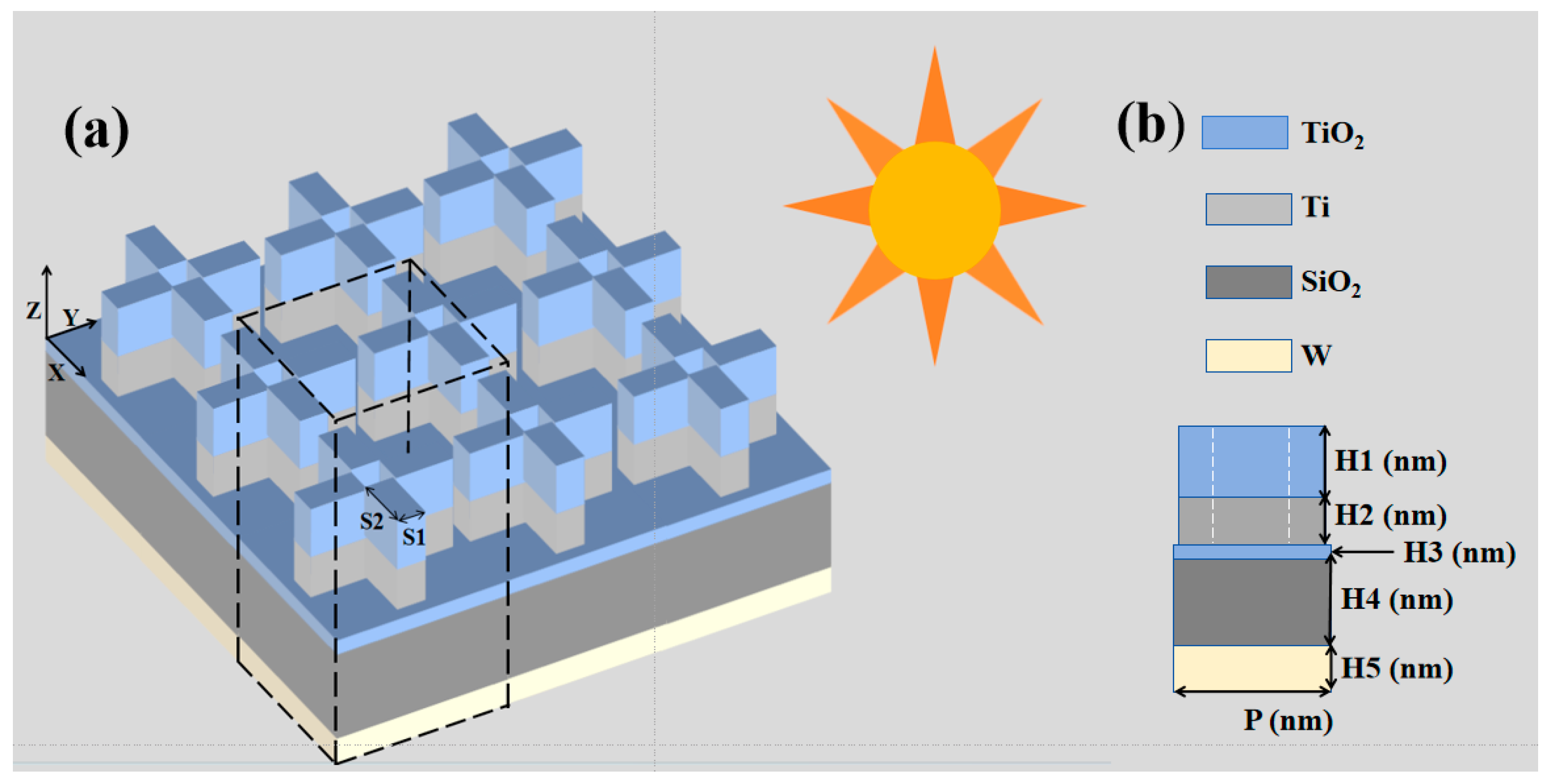
2. Structural Arrangement

In this paper, a five-layer cross-like structure of an ultra-broadband solar absorber is designed, see Figure 1, using metal W as the substrate, and SiO2, TiO2 films, Ti, and TiO2 are stacked on it. Simulations were performed by using FDTD. The following are the conditions to be met for various performance measurements. The light source in the paper is a plane wave with a wavelength of 280–4000 nm; set the periodic boundary conditions in the X and Y directions. And the mesh grid step length is 5 nm. The length and width of the underlying structure P = 500 nm, the short side length of the cross-like structure S1 = 120 nm, the long side length S2 = 160 nm, the thickness of each layer is H1 = 510 nm, H2 = 330 nm, H3 = 1 nm, H4 = 500 nm, and H5 = 250 nm. The absorption efficiency of the model is calculated by the following formula [41,42,43]:
A(λ) = 1 − R(λ) − T(λ)
R (λ) and T (λ) in this formula indicate their reflectivity and transmission, respectively [41]. Therefore, the desire to increase the absorption efficiency can be achieved by reducing the reflectance or reducing the transmission. Since the structure is a metal as the substrate, the transmission can be seen as zero, so the absorption efficiency can be approximated as 1-R. The manufacturing process is as follows: Wash the W substrate with acetone, alcohol, and deionized water, blow it dry, and enter the experimental manufacturing process. A certain thickness (500 nm) SiO2 film was deposited on a Cu substrate by magnetron sputtering, and then a Ti (1 nm)-TiO2 (330 nm)-Ti (510 nm) film was sequentially deposited on an ion beam. Finally, the desired microstructure is obtained by lithography and electron beam evaporation [44].

3. Analysis and Discussion of Results

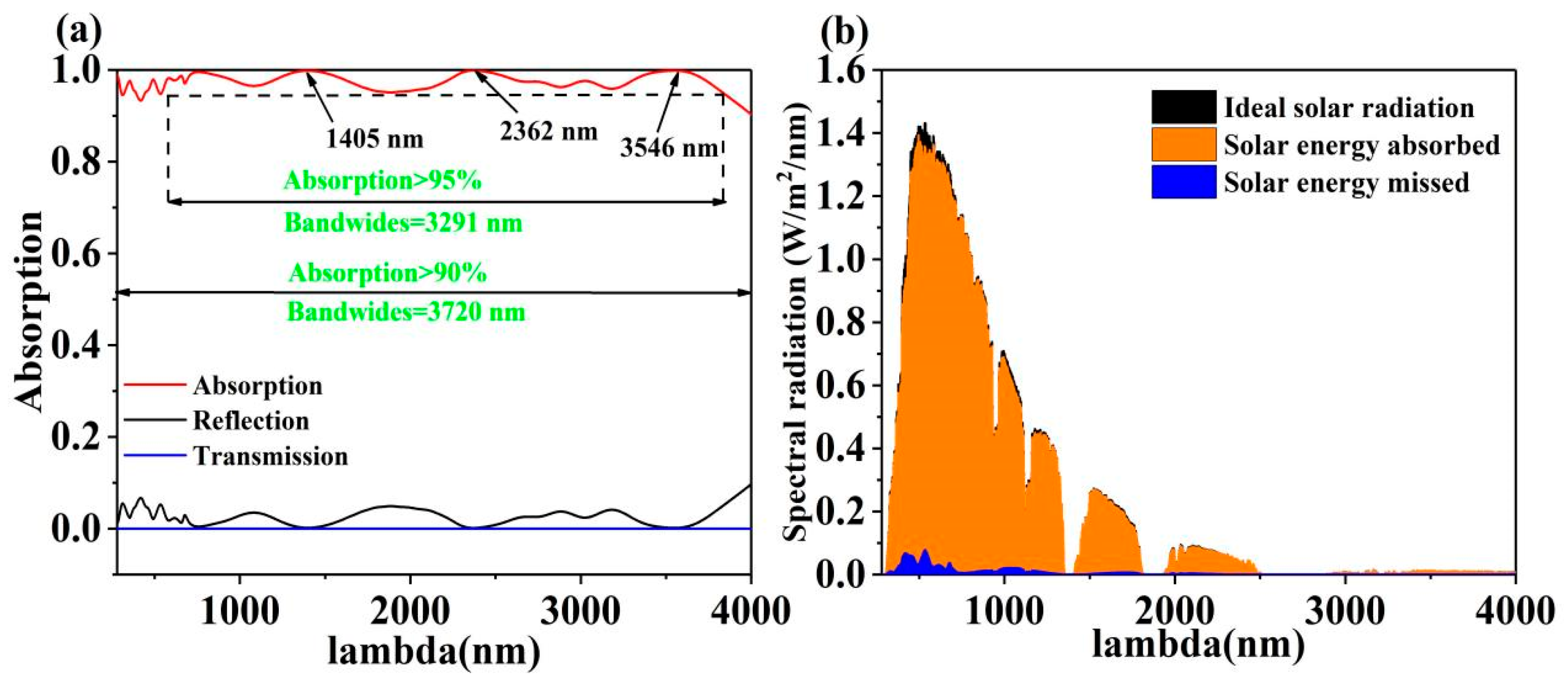
3.1. Broadband Absorption and Air Mass 1.5 Conditions

From Figure 2a, it is evident that the proposed structure maintains an absorption efficiency above 90% within the 280–4000 nm wavelength range. Furthermore, the absorption efficiency surpasses 95% within the 542–3833 nm wavelength range. We selected the three peaks with the highest absorption efficiency λ1 = 1405 nm, λ2 = 2362 nm, λ3 = 3546 nm, and we will analyze the field strength distribution of these three peaks later. The average absorption efficiency is an important index to measure the absorber performance, and its calculation formula is as follows [45,46]:
A a v g = λ m i n λ m a x A ( λ ) d λ λ m a x λ m i n
After the calculation of the above formula, the average absorption efficiency reaches 97.38% within the range from 280 nm to 4000 nm, and it is 97.75% in the range from 542 nm to 3833 nm.
AM represents air quality (Air Mass), the length of the path of the sun’s light through the atmosphere. For example, AM 0 refers to the reception of sunlight in outer space and is suitable for application scenarios such as satellites; AM 1 refers to the exposure of sunlight directly vertically to the earth’s surface. When sunlight enters the surface of the earth at different latitudes, it can define the atmospheric mass of other values to be AM = l/cosθ according to the different angles of incidence and the total optical range. In which, θ represents the Angle between sunlight and the ground normal. When θ = 48.2°, the atmospheric mass is AM 1.5, and its total radiation amount is 1 kW/m2.
At the air mass of 1.5, the mean absorption efficiency of solar energy can be determined using Equation (3). IAM1.5(λ) is the incident solar energy of the spectrum at the air mass of 1.5, and λmin λmax is equal to 280 nm and 4000 nm, respectively [47]:
α = λ m i n λ m a x I A M 1.5 ( λ ) A ( λ ) d λ λ m i n λ m a x I A M 1.5 ( λ ) d λ
In Figure 2b, orange represents the absorbed solar energy, black indicates the ideal solar radiation, and blue signifies the missed solar energy. The absorbed solar energy represents the portion of the incoming solar radiation that is effectively captured and utilized by a solar panel or other solar energy conversion system. On the other hand, the missed solar energy represents the portion of the incoming solar radiation that is not captured or utilized by the solar panel. Calculations show that the average absorption efficiency of solar energy is 97.46%, with a loss of 2.54% in absorption efficiency. This indicates that the structure exhibits high absorption efficiency.

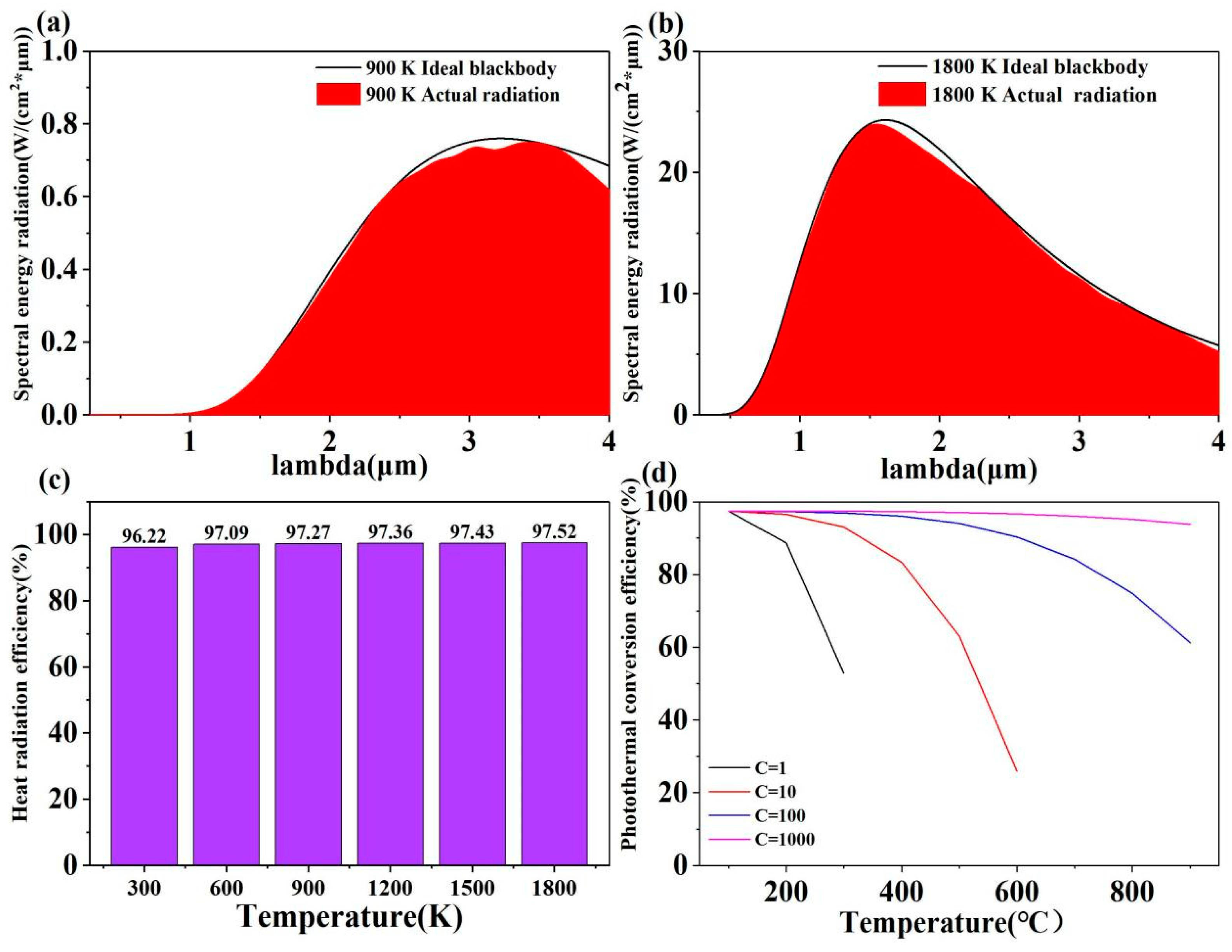
3.2. Thermal Radiation Efficiency and the pc Efficiency

Blackbody radiation refers to the electromagnetic radiation emitted by an object at thermal equilibrium. According to Planck’s law, the spectral distribution of blackbody radiation is related to the object temperature. High temperatures on the surface of solar absorbers cause them to emit more thermal radiation, including radiation at different wavelengths such as visible, infrared, and ultraviolet light. The functioning of solar absorbers may cause blackbody radiation to occur, thus causing the loss of heat energy [48]. Therefore, it is crucial to minimize this thermal radiation loss. The ideal blackbody radiation is calculated by the following formula [49]:
I B ( λ , T ) = 2 h c 2 λ 5 · 1 e h c / λ k T 1
The calculation of thermal radiation efficiency is calculated by the following Formula (5), where IB(λ, T) is the blackbody radiation energy density intensity [50].
ε = λ m i n λ m a x A ( λ ) · I B ( λ , T ) d λ λ m i n λ m a x I B ( λ , T ) d λ      
After the calculation of the above equation, the thermal radiation efficiency at 900 K reaches 97.27%, and at 1800 K reaches 97.52%. By comparing the data from these two temperature points, we can observe a slight increase in the thermal radiation efficiency as the temperature increases. That is, objects at high temperatures emit more electromagnetic waves, thus increasing their thermal radiation efficiency. The materials we used are as follows: W melting point of 3422 °C, SiO2 melting point of 1723 °C, Ti melting point of 1668 °C, and TiO2 melting point of 3362 °C. Therefore, this structure can theoretically reach 1800 K. Figure 3c illustrates that the thermal radiation efficiency does not change very much as the temperature increases from 300 K to 1800 K, which is because of the use of two high-temperature resistant materials, Ti and TiO2, to make the structure have high thermal radiation efficiency.
The pc efficiency is a crucial indicator for evaluating solar absorbers. Based on the energy conservation principle, it is calculated by the following formula [51]:
η = α G ε ( σ T w 4 σ T 0 4 ) G                      
where the calculation of α and ε has been described previously, G is the total incident radiation, C is the solar concentration coefficient, Tw is the operating temperature of the absorber, and T0 is the atmospheric temperature, which is specified here as 0 °C.
The pc efficiency under varying temperature and concentration conditions can be determined using the formula provided. This relationship is depicted in Figure 3d as a line graph. It is evident that the pc efficiency of the absorber significantly increases with higher concentration coefficients. At C = 1000, the pc efficiency exceeds 90% across the entire temperature range. However, at C = 100, the pc efficiency decreases markedly as the operating temperature rises from 100 °C to 900 °C. After 600 °C, the pc efficiency drops below 90%. At C = 10, the pc efficiency decreases dramatically with increasing temperature. After 300 °C, the pc efficiency drops below 90%. At C = 1, its pc efficiency decreases faster. In summary, the data demonstrates that the pc efficiency of the proposed absorber remains high at various temperatures.
This study involves a comparative analysis of various solar absorbers referenced across different sources, as detailed in the accompanying Table 1 [39,52,53,54,55]. The literature selected in the above table is all made through FDTD simulation, and the numerical calculation of the model is basically consistent with our paper. Each different structure exhibits a unique bandwidth characteristic while maintaining a high absorption efficiency. Considering the overall uneven absorption efficiency, we focus on comparing the absorption efficiencies of individual structures with efficiencies over 90%. As can be seen from the table, our structure outperforms the efficiency and bandwidth of the cited literature. As can be seen from the table, our structure is better than the efficiency and bandwidth of the cited literature. Moreover, we assessed how efficiently these models functioned at elevated temperatures. As can be observed from the tabular data [39,52,53], studies of thermal radiation efficiency were not addressed. At 1000 K, the thermal radiation efficiency of reference [54] was only 83.26%, while at 2000 K, the reference [55] was 91.47%. In contrast, the structures in this study are 97.27% at 900 K and 97.52% at 1800 K. Obviously, as the temperature increases, the thermal radiation efficiency also increases. Thus, the structure in this paper significantly outperformed the cited references in terms of thermal radiation efficiency.

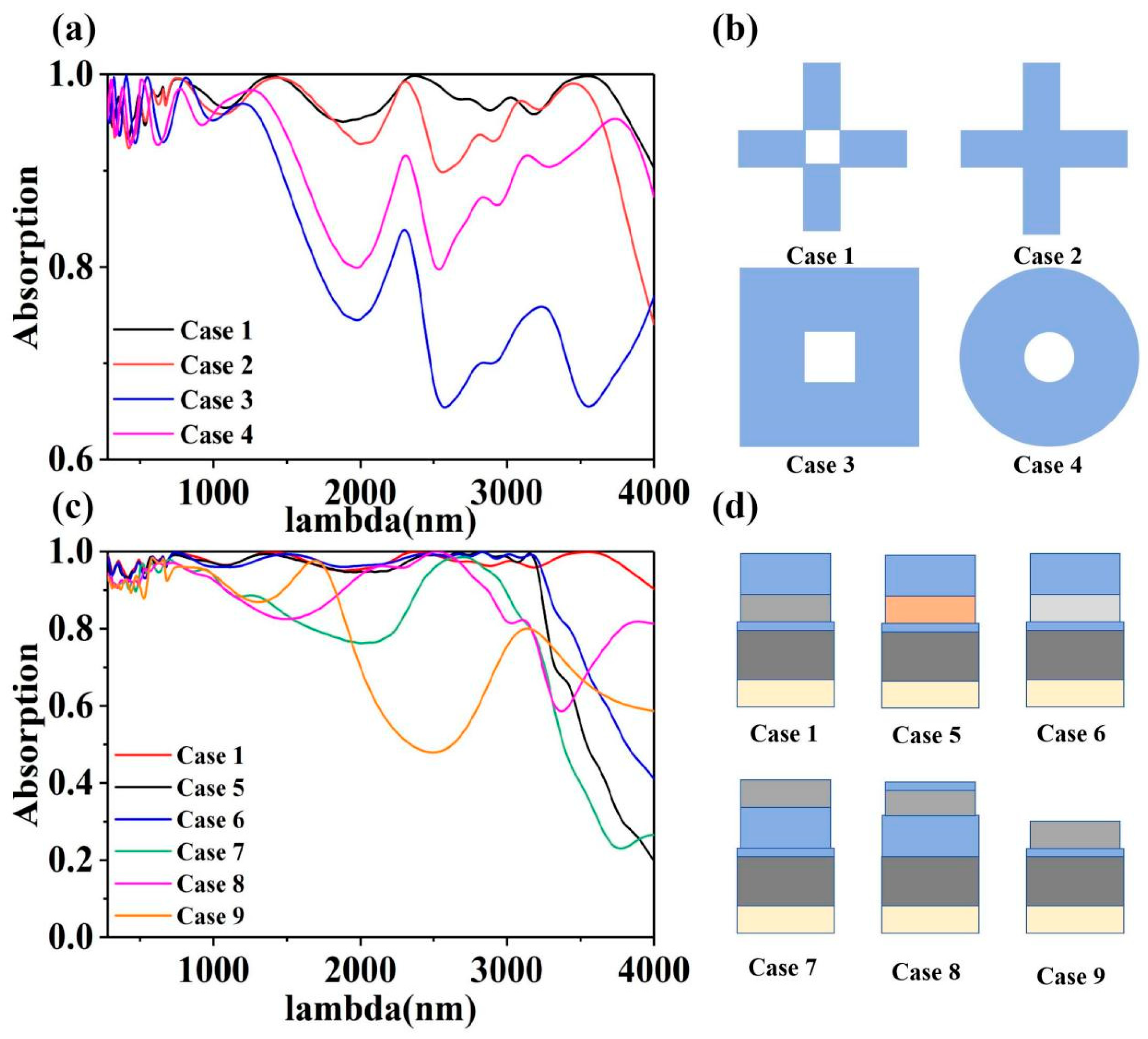
3.3. Different Structures Yield Distinct Outcomes

In Figure 4, we compared the absorption curves of nine different structures, where Figure 4b,d shows the changed structure. Case 2, case 3, and case 4 change the overall frame of the upper layer, case 5 and case 6 change the middle layer Ti to Ni and W, respectively, case 7, case 8, and case 9 change the order of its arrangement. In Figure 4a,c represents the absorption efficiency of these 9 structures. Since these two curves can only describe the basic trend and it is difficult to compare the size, in order to better compare the absorption efficiency of the different structures in Figure 4, we added the bar chart drawn in Figure 5 to describe them.
Figure 5a corresponds to the structure changed in Figure 4b and Figure 5b corresponds to the structure changed in Figure 4d. The pink column in Figure 5 indicates the average absorption efficiency of each structure at wavelengths 280–4000 nm, and the purple column indicates the thermal radiation efficiency of each structure at 2100 K. Our chosen Ti-TiO2-Ti cross structure has a unique symmetry and geometrical configuration that helps to realize the cavity coupling effect. When the frequency of the incident light matches the resonance frequency of the cross structure, a strong electric field resonance forms inside the structure, thus enhancing the light absorption and capture efficiency [56]. At the gap and intersection of the cross structure, regions of high electric field strength are formed due to the superposition effect of the electric field. These regions can significantly enhance light-matter interactions and enhance light absorption [57]. The cross structure can effectively capture the incident light and restrict it to the structure for multiple reflections and refractions, thus increasing the interaction time between light and matter and improving the absorption efficiency of light. Under the action of the cavity coupling effect, light can be transmitted and transmitted inside the cross structure, further promoting the absorption and utilization of light. In the cross structure, we chose the cross structure with Ti-TiO2-Ti with high heat resistance. When the frequency of the incident light matches the frequency of the free electron oscillation in the metal material, the local surface plasmon resonance (LSPR) effect is generated on the metal material surface, namely the surface plasmon resonance [58,59]. The LSPR effect can produce a strong electromagnetic field enhancement on the surface of metallic materials, namely “hot spots”. These hot spots can significantly increase the interaction strength of light and matter, thus enhancing the absorption efficiency of light. In the Ti-TiO2-Ti cross structure, the LSPR effect and the cavity coupling effect can work together to enhance the absorption efficiency of light. The near-field enhancement produced by the LSPR effect can be further superimposed with the electric field resonance generated by the cavity coupling effect to form a stronger electric field enhancement [60]. Through the overall comparison, it can be observed that the selected structure of the average absorption efficiency and thermal radiation efficiency is higher than several other structures; the only one with the same is case 2, but as shown in Figure 4a, case 2 bandwidth is not so long as our structure, so comprehensive case 1 is the most suitable of the nine structure.

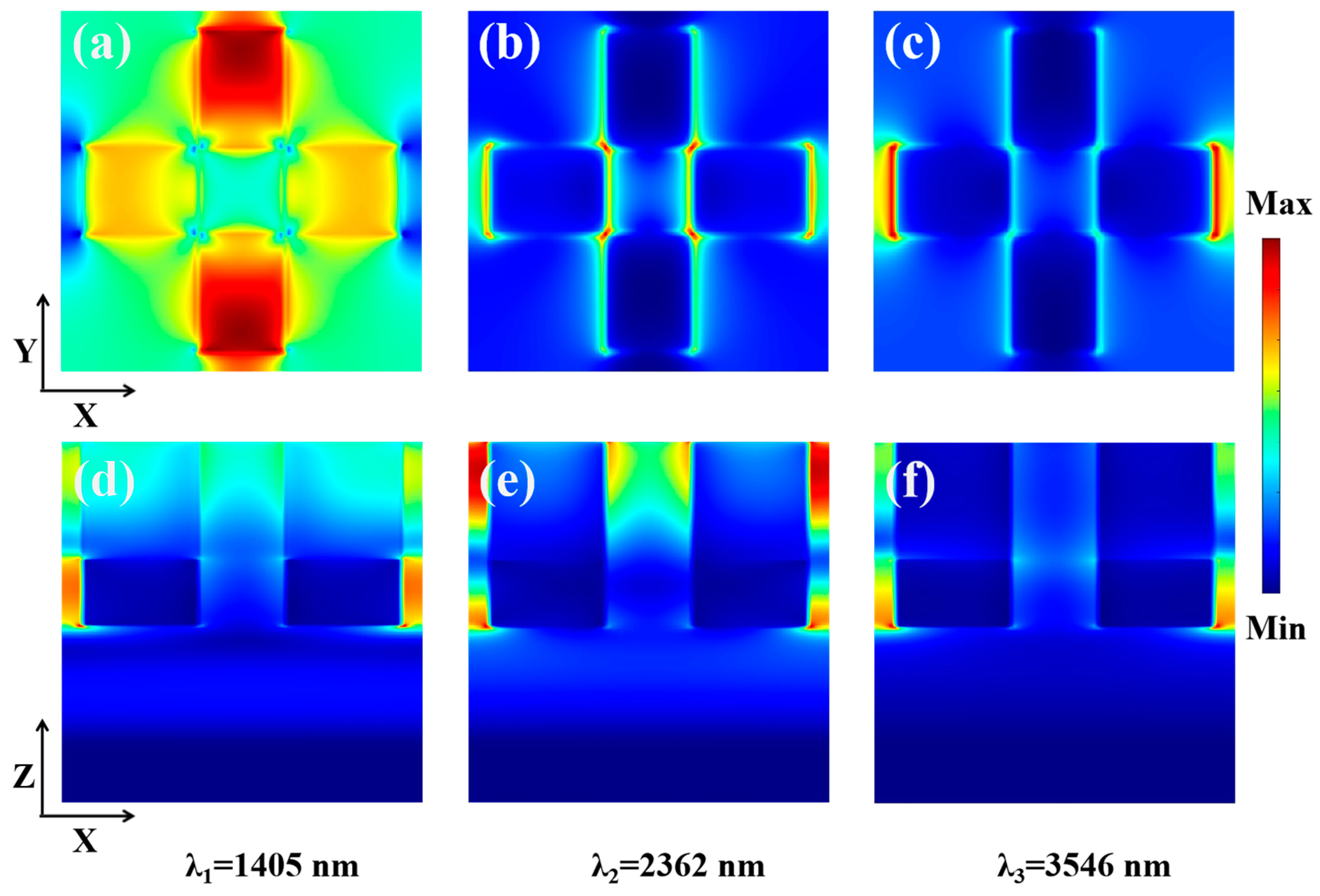
3.4. Field Strength Distribution
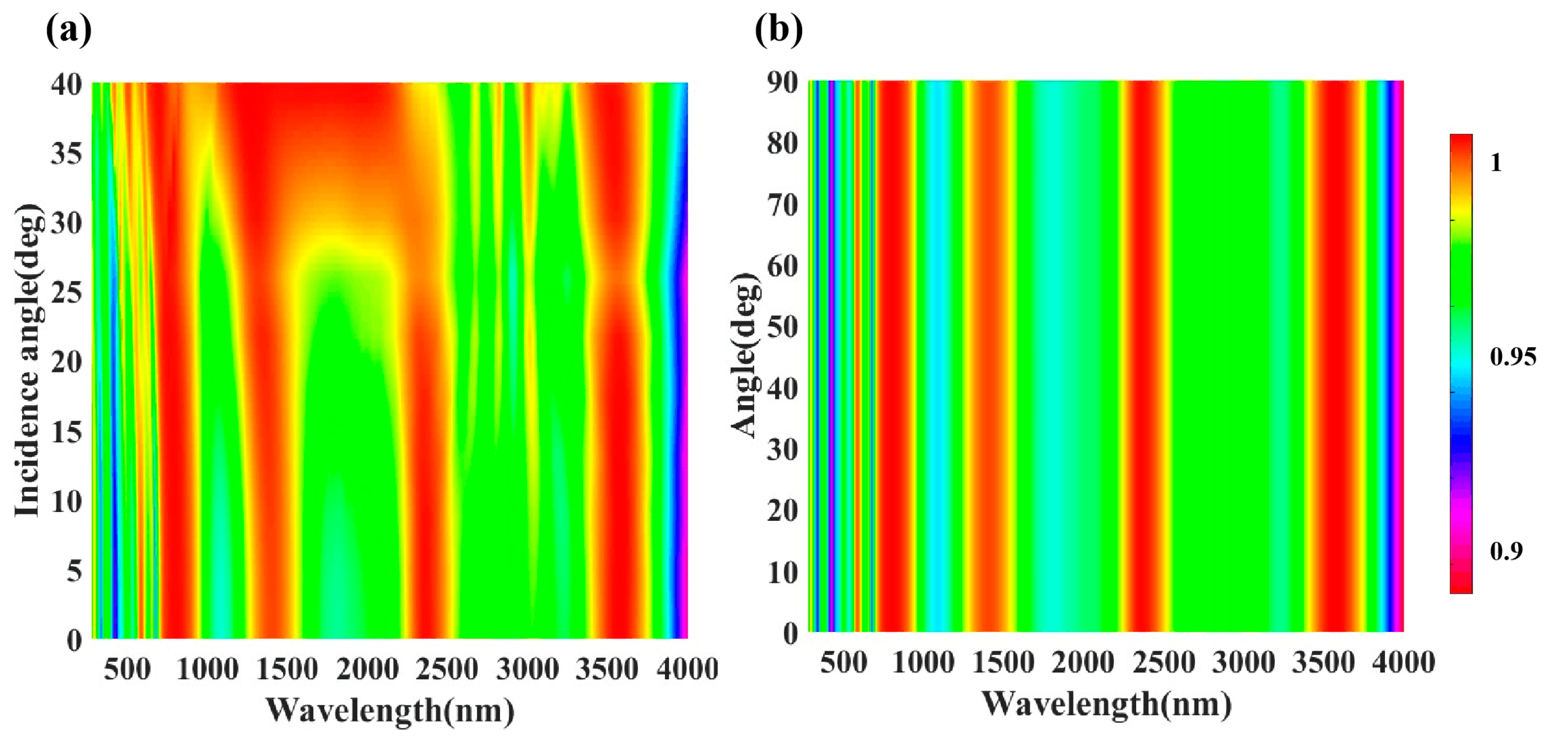
The electric field strength is also a key factor affecting the absorption efficiency. At the same material and frequency, the higher the electric field strength, the higher the absorption efficiency of the electromagnetic wave [61]. Figure 6a–c shows that at a wavelength of 1405 nm, the electric field is predominantly located on the surface of the TiO2 and along the edges of the cross structure. As the wavelength increases, TiO2 surfaces no longer have such a high electric field, and it is evenly distributed near the short edge of the cross structure, which is because of the excitation of LSPR at the resonance wavelength [62]. For further investigation, Figure 6d–f depicts the distribution of the electric field within the xoz plane. It is evident from Figure 6d–f that the electric field is higher in both the Ti layer and the TiO2 layer, and in Figure 6e, it is more intensely focused within the TiO2 layer. The electric field distribution observed here suggests the occurrence of the LSPR. Therefore, LSPR is the main reason for the longer absorption bandwidth of this absorber. The characteristics of the electric field distribution indicate that metal/dielectric stacked structures of different widths are excited into multiple surface isonic resonant modes under irradiation of incident light, thus allowing the structure to form a flat high absorption curve [63].

3.5. Angle Scanning

Figure 7a demonstrates that our symmetric structure enables the calculation of the absorption spectrum for increasing incidence angles from 0° to 40°. The spectral results are consistent with those shown in Figure 7a. When the angle of incidence is 0° to 40°, the absorption efficiency of the absorber is kept above 90%. However, after 40°, it’s not very sensitive to changes in angles. We can enhance the ability of the surface to capture sunlight by preparing micro-nano structures, such as nanoparticles and nanocones, on the surface of the solar absorber. These micro-nano structures can produce a surface plasmon resonance effect, making sunlight reflected and scattered repeatedly on the absorber surface, increasing the propagation path length of light, and thus improving the absorption efficiency of light. For large-angle incident sunlight, the surface of the micro-nano structure can better capture and absorb light and reduce reflection loss [64,65]. Figure 7b demonstrates that our symmetric structure enables the calculation of the absorption spectrum for polarization angles ranging from 0° to 90°. The absorption spectrum remains constant as the polarization angle increases. Therefore, we confirmed its polarization independence as well as angle insensitivity. It can be well applied to thermal electronics and earth electronics [66,67]. The incidence angle of sunlight will vary in different geographical locations and application scenarios. When selecting a solar absorber, the incidence angle range of sunlight should be evaluated according to the specific application scenario, and the absorber type and model suitable for the incidence angle range should be selected. For solar water heater systems installed on the roof, because the tilt angle of the roof is relatively fixed and usually small, we can use our proposed solar absorber [68].

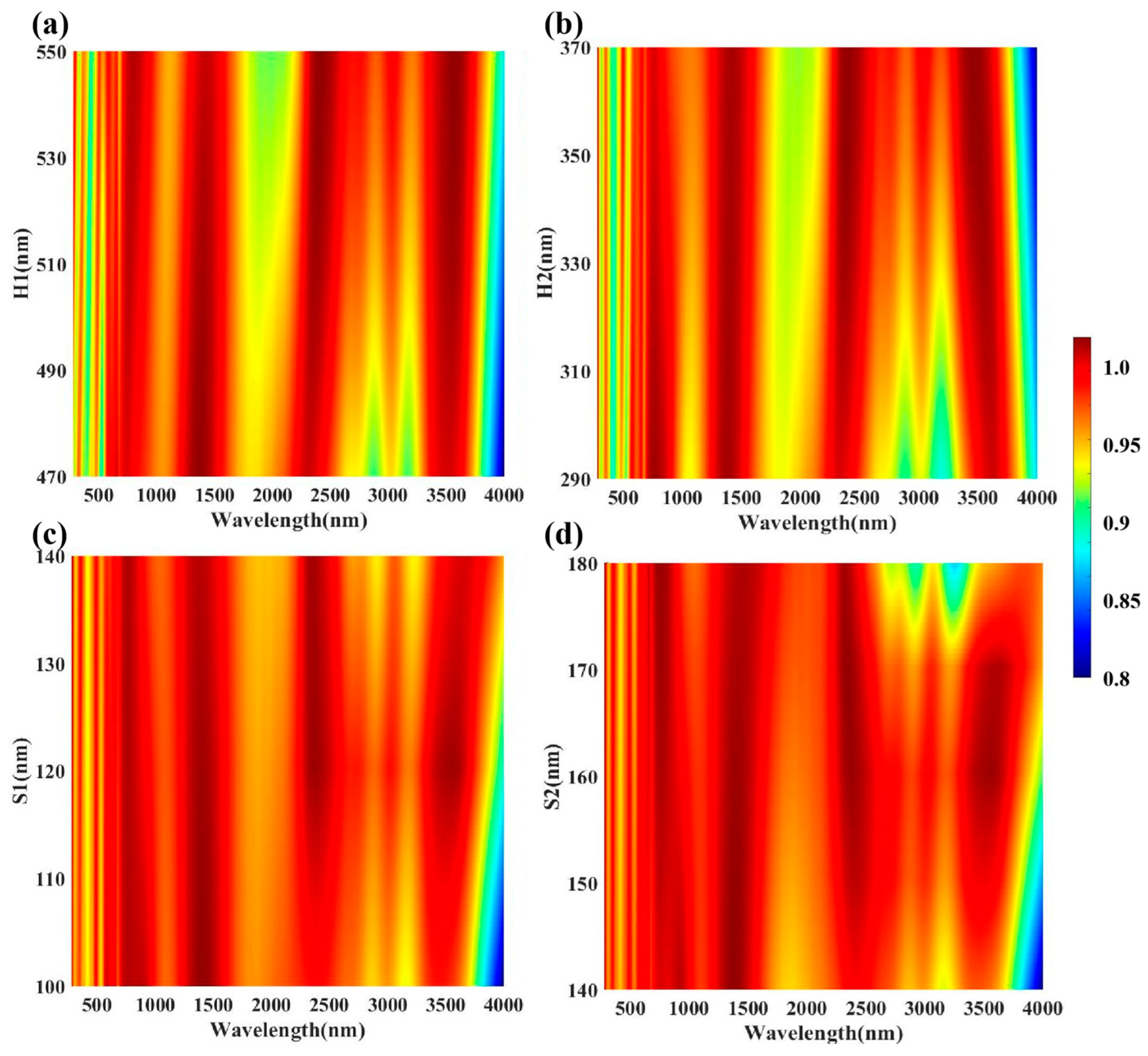
3.6. Different Structural Parameters Have Different Effects

Figure 8a illustrates the impact of varying thickness H1 on the absorption efficiency. As it is evident from Figure 8a, changes in thickness H1 up to approximately 800 nm have minimal influence on the absorption efficiency. Beyond 800 nm, the absorption efficiency increases with greater thickness H1 until around 1500 nm, after which it decreases as thickness H1 continues to increase. After exceeding 2500 nm, the absorption efficiency rises again with increasing thickness H1. Overall, more bands are enhanced by increased thickness H1 than are diminished, suggesting that a thicker structure may be beneficial. However, maintaining an overall average absorption efficiency is crucial. The intermediate value of 510 nm was also selected as the ultimate outcome. Figure 8b illustrates the effect of the variation in thickness H2 on the absorption efficiency. As it is evident from Figure 8b, the change in thickness H2 before 800 nm has no obvious influence on the absorption efficiency; 800–1000 nm absorption decreases with increasing thickness H2, 1000–1500 nm with increasing thickness H2, 1500–2500 nm again decreased with increasing thickness H2, 2500–3500 nm increased with increasing thickness H2, and 3500–4000 nm again decreased with increasing thickness H2. The increased band and the decreased band are generally poor. To balance the overall absorption efficiency of each wavelength. The median value of 330 nm was selected as the ultimate outcome. Figure 8c illustrates the influence of the change in the short side length S1 on the absorption efficiency, which has no obvious change before 2000 nm. Different from the thickness change, the band from 2500 nm to 3000 nm decreases from the middle length of 120 nm. In total, the absorption efficiency of the middle length 120 nm is generally higher than other lengths, so we chose 120 nm as the ultimate outcome. Figure 8d illustrates the effect of the change in the long side length S2 on the absorption efficiency. It is evident from Figure 8d that the middle length of 160 nm is approximately higher than 95%, and due to the influence of the process, more than this value is difficult to make, so we choose 160 nm as the ultimate outcome.

4. Error Analysis

The structure of the actual solar absorber may be very complex. In order to reduce the computational complexity, the model is usually simplified in simulation, such as by ignoring the irregularities of some microstructures, approximating the anisotropy of the material, etc. These simplifications can deviate from the simulation results and the actual situation. The accurate setting of the boundary conditions is crucial for the accuracy of the simulation results. In actual solar absorbers, the boundary conditions may be affected by various factors, such as the surrounding environment and installation method. However, in the simulation, it is often difficult to completely and accurately simulate these complex boundary conditions, and some approximate boundary conditions are usually adopted, such as periodic boundary conditions, symmetric boundary conditions, etc., which may introduce certain errors. Simulation requires accurate material parameters, such as refractive index, electrical conductivity, etc. However, the parameters of the actual materials may be affected by various factors, such as temperature, pressure, and preparation process, leading to some uncertainty in the material parameters. If the material parameters used are inaccurate, the accuracy of the simulation results is affected. In the numerical calculation, the limited range and accuracy of floating point numbers. As the computational steps increase, rounding errors may accumulate, affecting the accuracy of the simulation results. FDTD simulations usually require iterative calculations to solve the distribution of electromagnetic fields. During the iteration process, if the number of iterations is insufficient or the iteration algorithm is unstable, it may lead to iteration error and make the simulation results deviate from the true value [69,70,71].

5. Conclusions

This study introduces a solar absorber comprised of five layers of nanodisks based on a cross-like structure. At 280–4000 nm, structures are higher than 90% and have a bandwidth of 3720 nm. At 542–3833 nm, structures are even higher than 95% and have a bandwidth of 3291 nm. At the air mass of 1.5 (AM 1.5), the average absorption efficiency of solar energy is 97.46%, and the loss of solar energy is 2.54%, which has extremely high absorption efficiency. At the same time, its thermal radiation efficiency in a high-temperature environment is still good, especially at the temperature of 900 K; its thermal radiation efficiency can reach 97.27%, and at the extreme temperature of 1800 K, it can still maintain 97.52%, further highlighting Its excellent thermal stability and comprehensive performance. The pc efficiency of the proposed absorber can be maintained at high levels at different temperatures and can also be used in solar photovoltaic systems. Although simulations can provide rich information and accurate prediction results, the final validation still depends on experimental data. However, in obtaining accurate experimental data. In addition, there may be some differences between the experimental conditions and the simulation conditions, which makes the experimental verification results not completely match the simulation results, which increases the difficulty of evaluating the accuracy of the simulation results. In the future, we can strengthen cooperation with experimental research and obtain accurate data through experimental measurements for the calibration and verification of the simulation model. The research method combining experiment and simulation can complement and verify each other and improve the reliability and accuracy of the research results.

Author Contributions

Conceptualization, Z.Y., X.Y. and Q.S.; data curation, Z.Y., X.Y. and X.W.; formal analysis, Z.Y., X.Y. and X.W.; methodology, Z.Y., X.Y. and X.W.; resources, Z.Y., X.Y. and X.W.; software, X.W. and Q.S.; data curation, Z.Y., X.Y. and X.W.; writing—original draft preparation, Z.Y. and X.Y.; writing—review and editing, Z.Y., X.Y. and X.W. All authors have read and agreed to the published version of the manuscript.

Funding

The authors are grateful to the support provided by the National Natural Science Foundation of China (Nos. 51606158, 11604311, 12074151); the funding from the Natural Science Foundation of Fujian Province (2022J011102, 2022H0048); the funded from the Guangxi Science and Technology Base and Talent Special Project (No. AD21075009); the funding from the Sichuan Science and Technology Program (No. 2021JDRC0022); the funding from the Natural Science Foundation of Fujian Province (2022J011102); the funding from the Research Project of Fashu Foundation (MFK23006); the funding from the Open Fund of the Key Laboratory for Metallurgical Equipment and Control Technology of Ministry of Education in Wuhan University of Science and Technology, China (No. MECOF2022B01; MECOF2023B04); the funding from the Project supported by Guangxi Key Laboratory of Precision Navigation Technology and Application, Guilin University of Electronic Technology (No. DH202321); and the funding from the Scientific Research Project of Huzhou College (2022HXKM07).

Institutional Review Board Statement

Not applicable.

Informed Consent Statement

Not applicable.

Data Availability Statement

Publicly available datasets were analyzed in this study. These data can be found here: https://www.lumerical.com/ (accessed on 1 January 2020).

Conflicts of Interest

The authors declare no conflicts of interest.

References

  1. Chen, S.; Wu, X.H.; Fu, C.J. Active tuning of anisotropic phonon polaritons in natural van der Waals crystals with negative permittivity substrates and its application in energy transport. Opto-Electron. Sci. 2024, 3, 240002. [Google Scholar] [CrossRef]
  2. Baeva, M.; Gets, D.; Polushkin, A.; Vorobyov, A.; Goltaev, A.; Neplokh, V.; Mozharov, A.; Krasnikov, D.V.; Nasibulin, A.G.; Mukhin, I.; et al. ITO-free silicon-integrated perovskite electrochemical cell for light-emission and light-detection. Opto-Electron. Adv. 2023, 6, 220154. [Google Scholar] [CrossRef]
  3. Creutzig, F.; Agoston, P.; Goldschmidt, J.C.; Luderer, G.; Nemet, G.; Robert, C.P. The underestimated potential of solar energy to mitigate climate change. Nat. Energy 2017, 2, 17140. [Google Scholar] [CrossRef]
  4. Xiao, T.X.; Tu, S.; Liang, S.Z.; Guo, R.J.; Tian, T.; Müller-Buschbaum, P. Solar cell-based hybrid energy harvesters towards sustainability. Opto-Electron. Sci. 2023, 2, 230011. [Google Scholar] [CrossRef]
  5. Zhang, H.; Feng, L.; Wang, F.Y.; Liu, M.Z.; Zhang, Y.Y.; Zhu, J.; Lu, Y.; Xu, T. Janus aramid nanofiber aerogel incorporating plasmonic nanoparticles for high-efficiency interfacial solar steam generation. Opto-Electron. Adv. 2023, 6, 220061. [Google Scholar] [CrossRef]
  6. Colmenares-Quintero, R.F.; Rojas, N.; Colmenares-Quintero, J.C.; Stansfield, K.E.; Villar-Villar, S.S.; Albericci-Avendaño, S.E. Design of an Integral Simulation Model for Solar-Powered Seawater Desalination in Coastal Communities: A Case Study in Manaure, La Guajira, Colombia. Sustainability 2025, 17, 1505. [Google Scholar] [CrossRef]
  7. Basit, M.A.; Imran, M.; Anwar-Ul-Haq, T.; Yan, C.-F.; Breaz, D.; Cotîrlă, L.-I.; Danciu, A. Advancing Renewable Energy Systems: A Numerical Approach to Investigate Nanofluidics’ Role in Engineering Involving Physical Quantities. Nanomaterials 2025, 15, 261. [Google Scholar] [CrossRef]
  8. Xiao, Y.F.; Ma, C.; Sun, T.Y.; Song, Q.J.; Bian, L.; Yi, Z.; Hao, Z.Q.; Tang, C.J.; Wu, P.H.; Zeng, Q.D. Investigation of a high-performance solar absorber and thermal emitter based on Ti and InAs. J. Mater. Chem. A 2024, 12, 29145. [Google Scholar] [CrossRef]
  9. Esposito, S.; D’Angelo, A.; Diletto, C.; Rossi, G.; Volpe, R.; Guglielmo, A.; De Girolamo Del Mauro, A.; Prestigiacomo, C.; Lanchi, M. Solar Selective Absorber Coating with Ag Infrared Reflector for Receiver Tubes Operating at 550 °C. Energies 2025, 18, 880. [Google Scholar] [CrossRef]
  10. Sun, Y.B.; Yang, L.L.; Wang, J.X.; Cheng, Y.Z.; Luo, H.; Chen, F.; Li, X.C. Microstrip antenna loaded with focusing metasurface for high-gain dual-polarization and bidirectional radiation. J. Appl. Phys. 2025, 137, 013104. [Google Scholar] [CrossRef]
  11. Landy, N.I.; Sajuyigbe, S.; Mock, J.J.; Smith, D.R.; Padilla, W.J. Perfect Metamaterial Absorber. Phys. Rev. Lett. 2008, 100, 207402. [Google Scholar] [CrossRef] [PubMed]
  12. Yang, C.; Luo, M.H.; Ju, X.W.; Hu, J.Y. Ultra-narrow dual-band perfect absorber based on double-slotted silicon nanodisk arrays. J. Phys. D Appl. Phys. 2024, 57, 345104. [Google Scholar] [CrossRef]
  13. Gu, X.; Liu, X.; Yan, X.F.; Du, W.J.; Lin, Q.; Wang, L.L.; Liu, G.D. Polaritonic coherent perfect absorption based on self-hybridization of a quasi-bound state in the continuum and exciton. Opt. Express 2023, 31, 4691–4700. [Google Scholar] [CrossRef]
  14. Jo, Y.; Park, H.; Yoon, H.; Kim, I. Advanced biological imaging techniques based on metasurfaces. Opto-Electron. Adv. 2024, 7, 240122. [Google Scholar] [CrossRef]
  15. Tan, Z.Q.; Lin, Q.; Du, W.J.; Wang, L.L.; Liu, G.D. Simultaneously enhance electric and magnetic Purcell factor by strong coupling between toroidal dipole quasi-BIC and electric dipole. J. Appl. Phys. 2025, 137, 033103. [Google Scholar] [CrossRef]
  16. Wang, H.Y.; Ma, R.; Liu, G.D.; Wang, L.L.; Lin, Q. Optical force conversion and conveyor belt effect with coupled graphene plasmon waveguide modes. Opt. Express 2023, 31, 32422. [Google Scholar] [CrossRef]
  17. Li, W.X.; Cheng, S.B.; Yi, Z.; Zhang, H.F.; Song, Q.J.; Hao, Z.Q.; Sun, T.Y.; Wu, P.H.; Zeng, Q.D.; Raza, R. Advanced optical reinforcement materials based on three-dimensional four-way weaving structure and metasurface technology. Appl. Phys. Lett. 2025, 126, 033503. [Google Scholar] [CrossRef]
  18. Li, B.X.; Liu, M.L.; Wen, R.Q.; Wei, Y.; Zeng, L.L.; Deng, C.S. Dynamic control of Fano-like interference in the graphene periodic structure. J. Phys. D Appl. Phys. 2023, 56, 115104. [Google Scholar] [CrossRef]
  19. Liu, M.L.; Li, B.X.; Zeng, L.L.; Wei, Y.; Wen, R.Q.; Zhang, X.J.; Deng, C.S. Dynamic tunable narrow-band perfect absorber for fiber -optic communication band based on liquid crystal. J. Phys. D Appl. Phys. 2023, 56, 505102. [Google Scholar] [CrossRef]
  20. Hu, J.Y.; Tan, C.X.; Bai, W.D.; Li, Y.M.; Lin, Q.; Wang, L.L. Dielectric nanocavity-coupled surface lattice resonances for high-efficiency plasmonic sensing. J. Phys. D Appl. Phys. 2022, 55, 075105. [Google Scholar] [CrossRef]
  21. Wang, Q.S.; Fang, Y.; Meng, Y.; Hao, H.; Li, X.; Pu, M.; Ma, X.; Luo, X. Vortex-field enhancement through high-threshold geometric metasurface. Opto-Electron. Adv. 2024, 7, 240112. [Google Scholar] [CrossRef]
  22. Zhang, Y.X.; Lin, Q.; Yan, X.Q.; Wang, L.L.; Liu, G.D. Flat-band Friedrich-Wintgen bound states in the continuum based on borophene metamaterials. Opt. Express 2024, 32, 10669–10678. [Google Scholar] [CrossRef]
  23. Yang, J.P.; Tang, A.; Lian, B.W.; Xiong, Z.J.; Ma, Z.B.; Gu, N.T. Optimal multi-spectrum polarization detection with full-Stokes in a single channel by using standard retarders. Measurement 2025, 242, 116052. [Google Scholar] [CrossRef]
  24. He, M.Y.; Wang, Q.Q.; Zhang, H.; Xiong, J.; Liu, X.P.; Wang, J.Q. Analog electromagnetic induced transparency of T-type Si-based metamaterial and its applications. Phys. Scr. 2024, 99, 035506. [Google Scholar] [CrossRef]
  25. Wang, J.Q.; Sun, J.Y.; Sun, S.; Zhang, H.; Wang, Q.Q.; Yang, J.Y.; Mei, Y.W. Numerical simulation of electromagnetically induced transparency in composite metamaterial. Phys. Scr. 2025, 100, 025512. [Google Scholar] [CrossRef]
  26. Tang, C.J.; Nie, Q.M.; Cai, P.G.; Liu, F.X.; Gu, P.; Yan, Z.D.; Huang, Z.; Zhu, M.W. Ultra-broadband near-infrared absorption enhancement of monolayer graphene by multiple-resonator approach. Diam. Relat. Mater. 2024, 141, 110607. [Google Scholar] [CrossRef]
  27. He, Z.; Fang, D.; Yi, Y. Design of a Tunable Metamaterial Absorption Device with an Absorption Band Covering the Mid-Infrared Atmospheric Window. Photonics 2025, 12, 148. [Google Scholar] [CrossRef]
  28. Chen, Z.Y.; Cheng, S.B.; Zhang, H.F.; Yi, Z.; Tang, B.; Chen, J.; Zhang, J.G.; Tang, C.J. Ultra wideband absorption absorber based on Dirac semimetallic and graphene metamaterials. Phys. Lett. A 2024, 517, 129675. [Google Scholar] [CrossRef]
  29. Li, Y.M.; Tan, C.X.; Hu, J.Y.; Bai, W.D.; Zhang, R.L.; Lin, Q.; Zhang, Y.; Wang, L.L. Ultra-narrow band perfect absorbance induced by magnetic lattice resonances in dielectric dimer metamaterials. Results Phys. 2022, 39, 105730. [Google Scholar] [CrossRef]
  30. Xiang, T.; Sun, Z.; Wang, L.L.; Lin, Q.; Liu, G.D. Polarization independent perfect absorption of borophene metamaterials operating in the communication band. Phys. Scr. 2024, 99, 085519. [Google Scholar] [CrossRef]
  31. Hung, C.-C.; Lin, X.-Y.; Wu, T.-L.; Liao, S.-H.; Chen, H.-S.; Yang, C.-F. Investigation of an Ultra-Wideband Optical Absorber with the Bandwidth from Ultraviolet C to Middle Infrared. Photonics 2025, 12, 83. [Google Scholar] [CrossRef]
  32. Shen, Z.; Ni, J. Multi-Resonant Full-Solar-Spectrum Perfect Metamaterial Absorber. Nanomaterials 2024, 14, 1959. [Google Scholar] [CrossRef] [PubMed]
  33. Li, X.T.; Cai, X.D.; Liu, C.; Kim, Y.; Badloe, T.; Liu, H.; Rho, J.; Xiao, S. Cascaded metasurfaces enabling adaptive aberration corrections for focus scanning. Opto-Electron. Adv. 2024, 7, 240085. [Google Scholar] [CrossRef]
  34. Drymiskianaki, A.; Viskadourakis, Z.; Kenanakis, G. Hybrid Microwave/Solar Energy Harvesting System Using 3D-Printed Metasurfaces. Materials 2024, 17, 5969. [Google Scholar] [CrossRef] [PubMed]
  35. Wang, X.Y.; Lin, Q.; Wang, L.L.; Liu, G.D. Dynamic control of polarization conversion based on borophene nanostructures in optical communication bands. Phys. Scr. 2024, 99, 085531. [Google Scholar] [CrossRef]
  36. Jung, J.; Yoon, S.; Kim, B.; Kim, J.B. Development of High-Performance Flexible Radiative Cooling Film Using PDMS/TiO2 Microparticles. Micromachines 2023, 14, 2223. [Google Scholar] [CrossRef]
  37. Li, B.X.; Zeng, L.L.; Wen, R.Q.; Zhang, X.J. Dynamic Regulation of Multiple Fano Resonances Based on Liquid Crystal. IEEE Photonics J. 2023, 15, 2200506. [Google Scholar] [CrossRef]
  38. Zeng, L.L.; Li, B.X.; Wen, R.Q.; Zhang, X.J. Plasmonic Sensor Based on Multi Fano Resonance in Inverse T Shape Structure for Detection of CO2 Concentration. IEEE Photonics J. 2023, 15, 2201805. [Google Scholar] [CrossRef]
  39. Abdulkarem, H.M.A.; Dhruvik, A.; Shobhit, K.P.; Muhammad, I.; Khaled, A.; Meshari, A.; Ammar, A. Structural investigation of ultra–Broadband disk-shaped resonator solar absorber structure based on CNT–TiC composites for solar energy harvesting. Int. J. Therm. Sci. 2023, 192, 108414. [Google Scholar] [CrossRef]
  40. Yu, Z.; Li, M.; Xing, Z.; Gao, H.; Liu, Z.; Pu, S.; Mao, H.; Cai, H.; Ma, Q.; Ren, W.; et al. Genetic algorithm assisted meta-atom design for high-performance metasurface optics. Opto-Electron. Sci. 2024, 3, 240016. [Google Scholar] [CrossRef]
  41. Hu, J.Y.; Bai, W.D.; Tan, C.X.; Li, Y.M.; Lin, Q.; Wang, L.L. Highly electric field enhancement induced by anapole modes coupling in the hybrid dielectric-metal nanoantenna. Opt. Commun. 2022, 511, 127987. [Google Scholar] [CrossRef]
  42. Wang, B.X.; Wu, C.Y.; Duan, G.Y.; Xu, W.; Pi, F.W. Review of broadband metamaterial absorbers: From principles, design strategies, and tunable properties to functiona applications. Adv. Funct. Mater. 2023, 33, 2213818. [Google Scholar] [CrossRef]
  43. Mao, Y.; Zhang, H.; Xiong, J.; Liu, X.P.; Wang, Q.Q.; Wang, J.Q. Controlling of spontaneous emission of quantum dots based on hyperbolic metamaterials. J. Phys. D Appl. Phys. 2024, 57, 255111. [Google Scholar] [CrossRef]
  44. Chen, Y.; Zhang, S.M.; Tian, Y.; Li, C.; Huang, W.; Liu, Y.; Jin, Y.; Fang, B.; Hong, Z.; Jing, X. Focus control of wide-angle metalens based on digitally encoded metasurface. Opto-Electron. Adv. 2024, 7, 240095. [Google Scholar] [CrossRef]
  45. Li, Z.T.; Cheng, S.B.; Zhang, H.F.; Yang, W.X.; Yi, Z.; Yi, Y.G.; Wang, J.Q.; Ahmad, S.; Raza, R. Ultrathin broadband terahertz metamaterial based on single-layer nested patterned graphene. Phys. Lett. A 2025, 534, 130262. [Google Scholar] [CrossRef]
  46. Luo, M.H.; Hu, J.Y.; Li, Y.M.; Bai, W.D.; Zhang, R.L.; Lin, Q.; Wang, L.L. Anapole-assisted ultra-narrow-band lattice resonance in slotted silicon nanodisk arrays. J. Phys. D Appl. Phys. 2023, 56, 375102. [Google Scholar] [CrossRef]
  47. Kang, D.H.; Heo, H.S.; Yang, Y.H.; Seong, J.; Kim, H.; Kim, J.; Rho, J. Liquid crystal-integrated metasurfaces for an active photonic platform. Opto-Electron. Adv. 2024, 7, 230216. [Google Scholar] [CrossRef]
  48. Yan, X.F.; Lin, Q.; Wang, L.L.; Liu, G.D. Tunable strong plasmon–exciton coupling based modulator employing borophene and deep subwavelength perovskite grating. J. Phys. D Appl. Phys. 2023, 56, 435106. [Google Scholar] [CrossRef]
  49. Xiong, H.; Yang, Q.; Huang, Y.Z.; Deng, J.H. High-Efficiency Microwave Wireless Power Transmission via Reflective Phase Gradient Metasurfaces and Surface Wave Aggregation. ACS Appl. Mater. Interfaces 2024, 16, 60189–60196. [Google Scholar] [CrossRef] [PubMed]
  50. Zhu, J.; Deng, J.H.; Xiong, H. Tri-Band Metamaterial Absorber Based on a Three-Ring Coupled Structure. ACS Appl. Electron. Mater. 2024, 6, 9184–9193. [Google Scholar] [CrossRef]
  51. Deng, M.; Kanwal, S.; Wang, Z.; Cai, C.; Cheng, Y.; Guan, J.; Hu, G.; Wang, J.; Wen, J.; Chen, L. Dielectric Metasurfaces for Broadband Phase-Contrast Relief-Like Imaging. Nano Lett. 2024, 24, 14641–14647. [Google Scholar] [CrossRef]
  52. Yu, P.; Yang, H.; Chen, X.; Yi, Z.; Yao, W.; Chen, J.; Yi, Y.; Wu, P. Ultra-wideband solar absorber based on refractory titanium metal. Renew. Energy 2020, 158, 227–235. [Google Scholar] [CrossRef]
  53. Jiang, X.; Wang, T.; Zhong, Q.; Yan, R.; Huang, X. A Near-Ideal Solar Selective Absorber with Strong Broadband Optical Absorption from UV to NIR. Nanotechnology 2020, 31, 315202. [Google Scholar] [CrossRef] [PubMed]
  54. Chen, M.J.; He, Y.R. Plasmonic nanostructures for broadband solar absorption based on the intrinsic absorption of metals. Solar Energy Mater. Sol. Cells 2018, 188, 156–163. [Google Scholar] [CrossRef]
  55. Qin, F.; Xu, F.; Liu, J.W.; Hu, P.F.; Yi, Z.; Liu, L.; Yang, H.; Zhang, J.G.; Pan, M.; Wu, P.H. Broadband solar absorbers with excellent thermal radiation efficiency based on W–Al2O3 stack of cubes. Int. J. Therm. Sci. 2022, 179, 107683. [Google Scholar] [CrossRef]
  56. Zeng, Z.L.; Liu, H.F.; Zhang, H.F.; Cheng, S.B.; Yi, Y.G.; Yi, Z.; Wang, J.Q.; Zhang, J.G. Tunable ultra-sensitive four-band terahertz sensors based on Dirac semimetals. Photonics Nanostruct. Fundam. Appl. 2025, 63, 101347. [Google Scholar] [CrossRef]
  57. Li, Z.T.; Li, X.; Liu, G.D.; Wang, L.L.; Lin, Q. Analytical investigation of unidirectional reflectionless phenomenon near the exceptional points in graphene plasmonic system. Opt. Express 2023, 31, 30458. [Google Scholar] [CrossRef] [PubMed]
  58. Zun, J.; Wu, Z.; Fu, D.; Lu, G.; Hu, H. Novel optical switch and four-to-one data selector utilizing an MIM waveguide structure based on surface plasmon polaritons. Measurement 2025, 241, 115681. [Google Scholar] [CrossRef]
  59. Li, X.; Li, Z.T.; Wang, L.L.; Lin, Q. Unidirectional reflectionless propagation in borophene plasmonic metamaterials. J. Phys. D Appl. Phys. 2023, 57, 015103. [Google Scholar] [CrossRef]
  60. Ma, R.; Zhang, L.G.; Zeng, Y.; Liu, G.D.; Wang, L.L.; Lin, Q. Extreme enhancement of optical force via the acoustic graphene plasmon mode. Opt. Express 2023, 31, 482723. [Google Scholar] [CrossRef]
  61. Cheng, S.B.; Li, W.X.; Zhang, H.F.; Akhtar, M.N.; Yi, Z.; Zeng, Q.D.; Ma, C.; Sun, T.Y.; Wu, P.H.; Ahmad, S. High sensitivity five band tunable metamaterial absorption device based on block like Dirac semimetals. Opt. Commun. 2024, 569, 130816. [Google Scholar] [CrossRef]
  62. Ling, Z.X.; Zeng, Y.; Liu, G.D.; Wang, L.L.; Lin, Q. Unified model for plasmon-induced transparency with direct and indirect coupling in borophene-integrated metamaterials. Opt. Express 2022, 30, 21966. [Google Scholar] [CrossRef] [PubMed]
  63. Berhe, A.M.; As’ham, K.; Al-Ani, I.; Hattori, H.T.; Miroshnichenko, A.E. Strong coupling and catenary field enhancement in the hybrid plasmonic metamaterial cavity and TMDC monolayers. Opto-Electron. Adv. 2024, 7, 230181. [Google Scholar] [CrossRef]
  64. Li, W.; Cheng, S.; Zhang, H.; Yi, Z.; Tang, B.; Ma, C.; Wu, P.; Zeng, Q.; Raza, R. Multi-functional metasurface: Ul-tra-wideband/multi-band absorption switching by adjusting guided mode resonance and local surface plasmon resonance effects. Commun. Theor. Phys. 2024, 76, 065701. [Google Scholar] [CrossRef]
  65. Huang, Z.; Liu, G.D.; Wang, L. Active modulation of quasi-bound state in the continuum based on bulk Dirac semimetals metamaterial. Appl. Phys. Express 2022, 15, 032006. [Google Scholar] [CrossRef]
  66. Yang, C.; Lin, Q.; Du, W.J.; Wang, L.L.; Liu, G.D. Bi-tunable absorber based on borophene and VO2 in the optical telecom-munication band. J. Opt. Soc. Am. B 2022, 39, 2969–2974. [Google Scholar] [CrossRef]
  67. Li, W.; Yi, Y.; Yang, H.; Cheng, S.; Yang, W.X.; Zhang, H.; Yi, Z.; Yi, Y.; Li, H. Active Tunable Terahertz Band-width Absorber Based on single layer Graphene. Commun. Theor. Phys. 2023, 75, 045503. [Google Scholar] [CrossRef]
  68. Zeng, Y.; Ling, Z.X.; Liu, G.D.; Wang, L.L.; Lin, Q. Tunable plasmonically induced transparency with giant group delay in gain-assisted graphene metamaterials. Opt. Express 2022, 30, 455954. [Google Scholar] [CrossRef]
  69. Yan, X.; Lin, Q.; Wang, L.; Liu, G.D. Active absorption modulation by employing strong coupling between magnetic plasmons and borophene surface plasmons in the telecommunication band. J. Appl. Phys. 2022, 132, 063101. [Google Scholar] [CrossRef]
  70. Xiao, Y.T.; Chen, L.W.; Pu, M.B.; Xu, M.F.; Zhang, Q.; Guo, Y.; Chen, T.; Luo, X. Improved spatiotemporal resolution of an-ti-scattering super-resolution label-free microscopy via synthetic wave 3D metalens imaging. Opto-Electron. Sci. 2023, 2, 230037. [Google Scholar] [CrossRef]
  71. Alsaif, H.; Muheki, J.; Ben Ali, N.; Ghachem, K.; Surve, J.; Patel, S.K. Thin-Film Solar Energy Absorber Structure for Window Coatings for Self-Sufficient Futuristic Buildings. Micromachines 2023, 14, 1628. [Google Scholar] [CrossRef] [PubMed]
Figure 1. (a) illustrates the fundamental structure of the solar absorber. (b) shows its cross-sectional view with specific dimensions.
Coatings 15 00243 g001
Figure 2. (a) shows the absorption, reflection, and transmission curves of the solar absorber. (b) Illustrates the absorption profile of the absorber under an air mass of 1.5.
Coatings 15 00243 g002
Figure 3. (a) The black radiation diagram at 900 K. (b) The black radiation diagram at 1800 K. (c) The efficiency of thermal radiation for the structure at various temperatures. (d) The curve diagram illustrates the pc efficiency of the absorber under different solar concentration coefficients and temperatures.
Coatings 15 00243 g003
Figure 4. (a) is the absorption efficiency plot of the four different structures changing the upper overall frame; (b) is the top view corresponding to the four structures shown in (a); (c) is the absorption efficiency plot of the six different structures of the materials used and changed; (d) is the side view of the six structures corresponding to (c).
Coatings 15 00243 g004
Figure 5. (a) shows the index analysis of the altered superstructure. (b) shows the index analysis of the altered material and location.
Coatings 15 00243 g005
Figure 6. (ac) illustrates the distribution of the electric field within the three selected absorption bands in the xoy direction; (df) illustrates the distribution of the electric field within the three selected absorption bands in the xoz direction.
Coatings 15 00243 g006
Figure 7. (a) shows the absorption spectrum as the incidence angle increases from 0° to 40°. (b) shows the absorption spectrum as the polarization angle increases from 0° to 90°.
Coatings 15 00243 g007
Figure 8. (a) shows the distribution of thickness H1 changing from 470 nm to 550 nm; (b) shows the distribution of thickness H2 of the metal Ti varying from 290 nm to 370 nm; (c) Shows the short side length S1 changing from 100 nm to 140 nm; (d) Shows the long side length S2 changing from 140 nm to 180 nm.
Coatings 15 00243 g008
Table 1. Comparing data from various sources in the literature.
MemberAbsorption Bandwidth with a Rate Exceeding 90%Absorption EfficiencyThermal Radiation Efficiency
[52]1900 nm (100–2000 nm)93.17% (100–2000 nm)/
[53]712 nm (354–1066 nm)97% (354–1066 nm)/
[39]2800 nm (200–3000 nm)93.8% (280–2030 nm)/
[54]1200 nm (300–1500 nm)91% (300–1500 nm)83.26% (1000 K)
[55]1692 nm (420–2112 nm)93.16% (280–2500 nm)91.47% (2000 K)
proposed3720 nm (280–4000 nm)97.38% (280–4000 nm)
97.75% (542–3833 nm)
97.27% (900 K)
97.52% (1800 K)
Disclaimer/Publisher’s Note: The statements, opinions and data contained in all publications are solely those of the individual author(s) and contributor(s) and not of MDPI and/or the editor(s). MDPI and/or the editor(s) disclaim responsibility for any injury to people or property resulting from any ideas, methods, instructions or products referred to in the content.

