Article

Optical Coating Deposition on Submicron-Patterned Surfaces

Center for Physical Sciences and Technology (FTMC), Savanoriu Ave. 231, LT-02300 Vilnius, Lithuania
*
Author to whom correspondence should be addressed.
Coatings 2025, 15(4), 372; https://doi.org/10.3390/coatings15040372
Submission received: 1 March 2025 / Revised: 14 March 2025 / Accepted: 18 March 2025 / Published: 22 March 2025
(This article belongs to the Special Issue Optical Coatings: From Materials to Applications)

Abstract

:
Periodically modulated optical coatings, fabricated by depositing conformal films on modulated substrates, offer unique capabilities for spectral and spatial filtering of light. However, conventional deposition methods often do not achieve required replication and conformality on submicron-size structured surfaces. In this paper, we compare various thin film deposition techniques, including electron beam evaporation, atomic layer deposition, and ion beam sputtering, to evaluate their ability to control multilayer coating growth on periodically modulated substrates. Our study demonstrates that both single-layer and multilayer coatings produced by ion beam sputtering effectively replicate the initial geometry of structured surfaces, thereby enhancing optical performance.

1. Introduction

The increasing demand for more complex and higher-power, yet smaller, optical systems drives the need to advance optical coating fabrication technologies. Therefore, the growing demand for high-quality metamaterials can also be fulfilled by optical coating technologies to form photonic structures for spatial filtering [1,2], polarization control at zero angle of light incidence [3,4], etc. Such structures can be directly applied to increase the performance of microchip or ceramic lasers [5,6].
Current optical coating technologies for laser elements are well developed for producing high-quality and uniform films on flat or slightly curved substrates. However, modern optical and laser systems increasingly demand optical coatings on complex and structured surfaces. Recent advances in lithography and etching techniques have enabled the fabrication of intricate surface geometries [7,8] that often require dielectric and metallic coatings to achieve functionalities such as polarization control [9], selective absorption [10], and spectral or spatial filtering [11,12]. Therefore, methods are needed to produce coatings that precisely replicate the original substrate geometry. Conventional deposition techniques often face limitations related to coating thickness, as planarization of structured surfaces frequently occurs with increasing film thickness [13].
Additionally, modulation depth introduces distinct challenges. For shallow groove depths, increasing the film thickness flattens the modulation, while for highly corrugated surfaces, excessive coating thickness can lead to crack formation [14,15]. Moreover, different deposition techniques provide varying levels of conformality due to differences in the kinetic energy of deposited atoms. Low-energy processes, such as evaporation, exhibit limited surface diffusion, resulting in a porous coating structure. In contrast, higher-energy processes, such as ion-assisted deposition or ion beam sputtering, lead to denser and more conformal coatings [15]. Moreover, due to the high energy of sputtered atoms and the formation of dense films, ion beam sputtering is widely used not only for depositing optical coatings but also for the fabrication of optoelectronic and semiconductor devices [16,17,18].
The autocloning method has been proposed as an alternative for achieving replicating coatings on modulated substrates [19]. This technique combines thin film deposition and etching, and it has been applied to produce space-variant optical elements [9,20], spectral filters [21,22], omni-directional [23], high-reflection mirrors [22], etc. However, this process is complex and requires precise deposition and etching parameter optimization. Atomic layer deposition (ALD) is another promising approach. The ALD technique is based on gas phase sequential self-limiting surface reactions that enable conformal film growth [24]. It has been applied to coat high-aspect-ratio structures, such as nano-scale holes and trenches [25,26]. Also, such technology is used to form antireflective coatings, thereby enhancing the optical performance and surface quality of complex micro-optics [27].
The primary aim of this paper is to test several widely used deposition techniques for producing thick (few μm) multilayer coatings on periodically modulated surfaces and to identify the most promising method for nanostructured optical coatings. In this work, we investigated electron beam (E-beam) evaporation, plasma-assisted electron beam evaporation, ion beam sputtering (IBS), and atomic layer deposition (ALD). Initially, we evaluated the replication of the substrate’s surface geometry after the deposition of multilayer coatings using these techniques. Subsequently, the most promising technology to form layers on modulated substrates was investigated in detail.

2. Materials and Methods

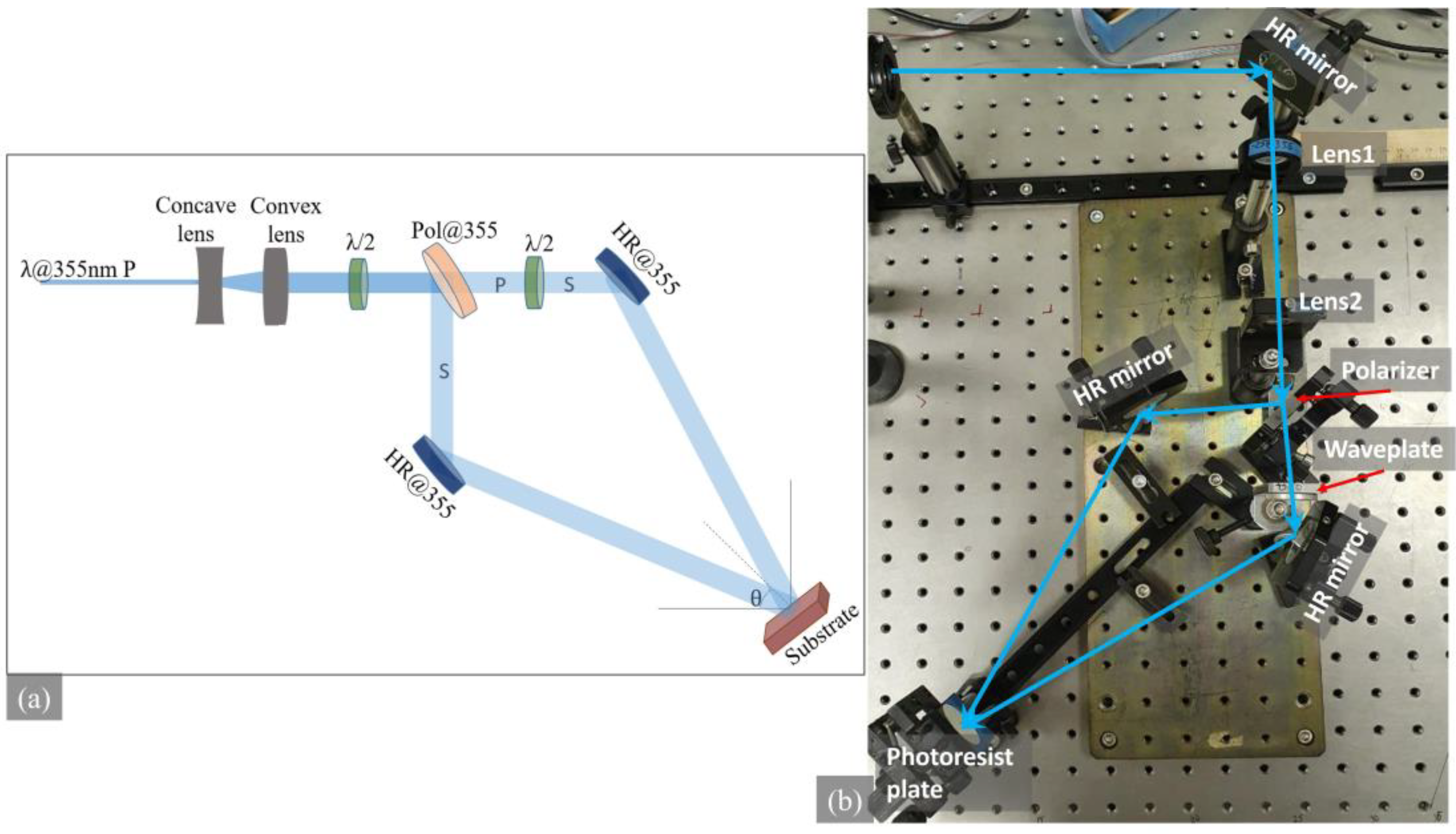
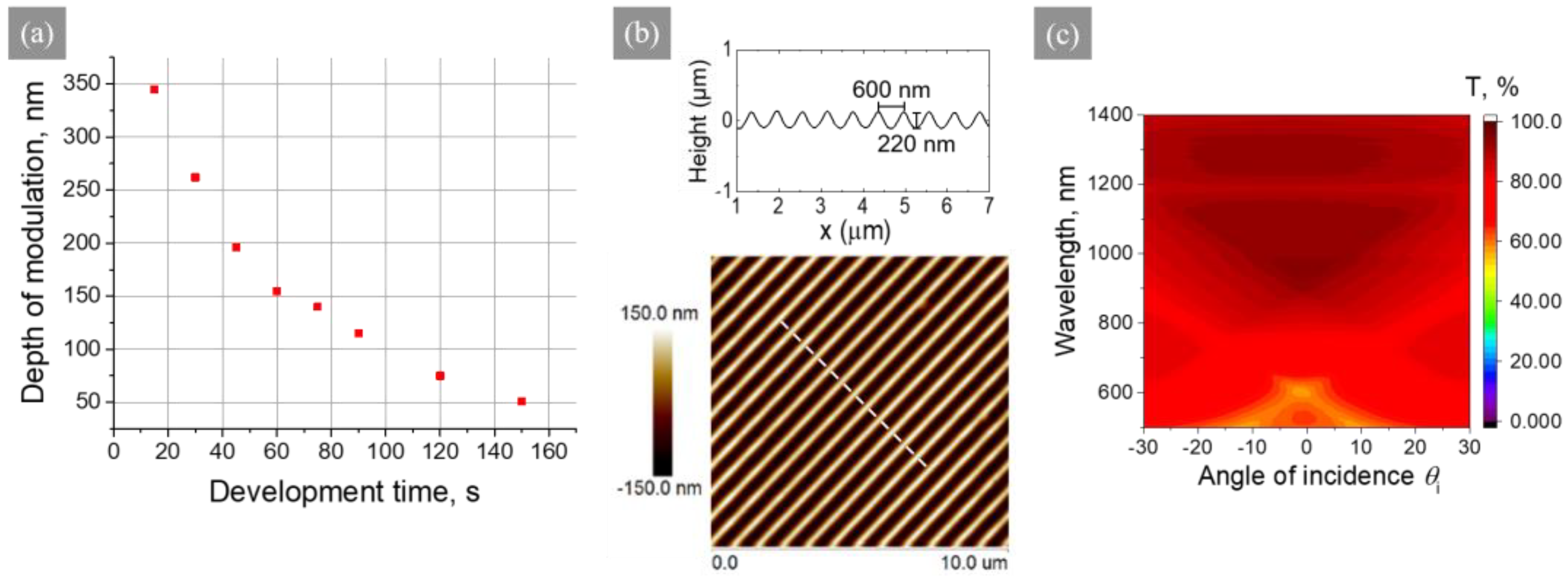
2.1. Fabrication of Modulated Substrates

Periodically modulated surfaces were produced by combining laser interference lithography and nanoimprint technology. The fabrication process comprised several steps: (i) preparing a master copy in a photoresist via interference lithography, (ii) fabricating a stamp from the master structure, and (iii) imprinting the master structure onto a substrate using a UV-curable polymer. Laser interference lithography was performed using the third harmonic (355 nm wavelength) of a Nd:YAG nanosecond laser (Ekspla, Vilnius, Lithuania) to create a master grating on the photoresist surface. In our case, an incident angle (θ) of approximately 16 degrees produced a grating periodicity of 600 nm (Figure 1).
The positive photoresist was exposed to a total energy of 0.44 mJ and subsequently developed in a KOH solution. As illustrated in Figure 2a, the grating modulation depth varied with the development time, ranging from 350 nm to 50 nm as the time increased from 15 s to 150 s.
The typical grating geometry and transmittance spectra are shown in Figure 2b,c, respectively. Gratings with a period of 600 nm and a 200–220 nm depth were selected as a suitable substrate structure for further experiments. The master structure was then covered by Ni coating and used in a soft nanoimprint lithography process to fabricate copies using a UV-cured polymer (OrmoComp®, nref = 1.52). Such samples with periodically modulated surfaces are transparent even in the UV spectral range, without low transmittance zones, and indicate sufficient quality for further coating deposition experiments.

2.2. Coatings Deposition Techniques

2.2.1. E-Beam with Glancing Angle Deposition

Electron beam evaporation with glancing angle deposition (GLAD) was employed to produce all-silica multilayer coatings on periodically modulated substrates. This technology is known to be used as a replication method and also in high-power optic fabrication [3]. In these experiments, alternating porous and dense SiO2 layers were deposited at 0° and 70° angles, resulting in effective refractive indices of 1.41 and 1.25, respectively. The substrate was continuously rotated during the deposition. The deposition rate was 3 Å/s and was monitored using a quartz crystal microbalance. In this work, the multilayer coatings were deposited using a Sidrabe system equipped with a stepper motor system for the GLAD method. The chemical composition of SiO2 coatings produced via GLAD method is reported elsewhere [3].

2.2.2. E-Beam with Plasma Assistance

Electron beam evaporation with plasma assistance to enhance the kinetic energy of evaporated atoms was used for the deposition process. Multilayer coatings consisting of Al2O3 and SiO2 layers were deposited on structured substrates. Two approaches were tested: one with continuous substrate rotation in a calotte and the other with the stationary sample positioned above the plasma source. No additional heating was used during the process. Typically, Al2O3 films deposited at room temperature are amorphous and stoichiometric [28]. The plasma-assisted evaporation experiments were performed using a radio-frequency (RF)-driven Copra IS300 plasma source IS 300 (CCR GmbH, Troisdorf, Germany) installed in electron beam deposition plant Vera 1100 (VTD Vakuumtechnik Dresden GmbH, Dresden, Germany) [29]. Ion energy can be adjusted to the maximum of ≈350 eV, and more technical details can be found here [30]. In our setup, the substrates were placed in a calotte approximately 40 cm from the plasma source, and parameters were tuned to reach ion energies of about 150 eV. A gas flow of 40 sccm O2 was supplied through the plasma source, with an additional 20 sccm O2 used to maintain a pressure of 1.2 × 10⁻⁴ mbar during deposition. Deposition rates for Al2O3 and SiO2 granular materials (Umicore) were kept at 3 Å/s.

2.2.3. Ion Beam Sputtering

The IBS coatings were deposited using an ion beam sputtering (IBS) system developed by Cutting Edge Coatings GmbH (Hannover, Germany) [31]. The parameters of coating machine and thickness monitoring are described in detail elsewhere [32]. The IBS system consists of a single inductively coupled 8.5 cm diameter multiaperture ion source [33]. The material target is located approximately 31 cm at the central part from the ion source and tilted by ~55°. The substrates are located 15–30 cm above the target depending on the position on a rotating calotte position. During the deposition process, the ion source was supplied only with Ar ions, while reactive oxygen was introduced directly into the chamber through a separate reactive gas inlet. The acceleration voltage of the primary ion source ranged from 1000 V to 1100 V, with slight variations depending on the target material. Multilayer coatings consisting of Ta2O5 and SiO2 were produced by reactive IBS (total physical thickness was about 2.4 µm). Additionally, in further experiments, 1 µm thick single-layer coatings of HfO2, Ta2O5, Nb2O5, and SiO2 were deposited. Deposition parameters for all single-layer films are summarized in Table 1; no additional substrate heating was used. The layers’ chemical composition was not investigated in this research but can be found elsewhere, e.g., [34,35].

2.2.4. Atomic Layer Deposition

Multilayer coating consisting of 17 alternating HfO2 and Al2O3 layers, with individual layer thicknesses of 85.6 nm and 109.4 nm, respectively, was deposited by ALD. HfO2 was grown as a nanolaminate, with an interlayer of Al2O3 inserted after every 186 cycles of hafnia to suppress the crystallization. Similar nanolaminate thin films have been reported to reduce crystallization [36]. The precursors used for HfO2 and Al2O3 were tetrakis(dimethylamino)hafnium (TDMAH) and trimethylaluminum (TMA), respectively, with water used as the oxidizer. TDMAH cylinder was maintained at 75 °C. The ALD cycle for HfO2 comprised 0.2 s of TDMAH pulse and 0.02 s of water pulse, with purge durations of 5 s between pulses. The ALD cycle for Al2O3 consisted of 0.02 s TMA and water pulses, with purge durations of 5 s between the precursor and oxidizer pulses. Nitrogen was used as the carrier, and purge gas occurred at flow rates of 90 sccm and 20 sccm for HfO2 and Al2O3 depositions, respectively. Depositions were carried out at 120 °C using a Veeco Savannah S200 ALD system. According to the literature, HfO2 and Al2O3 films deposited by ALD under similar process conditions exhibit a stoichiometric composition [37,38].

2.3. Characterization

Surface and cross-sectional morphologies of structured surfaces were evaluated using scanning electron microscopy (SEM; Helios Nanolab 650 system) and atomic force microscopy (AFM; Dimension Edge of Bruker system). AFM scan area was 10 µm × 10 µm. Refractive indices and extinction coefficients were determined by OptiChar V.15.12b software (OptiLayer Gmbh, Hanau, Germany) using transmittance and reflectance spectra measured by spectrophotometer Photon RT (EssentOptics, Vilnius, Lithuania).

3. Results and Discussion

3.1. Investigation of Different Deposition Techniques

Various thin film deposition techniques were systematically evaluated to produce a replication of periodically modulated substrates after multilayer coating fabrication. In particular, thick multilayer coatings, several micrometers in thickness, were deposited using various deposition methods, including electron beam evaporation with GLAD or plasma assistance, atomic layer deposition, and ion beam sputtering. Cross-sectional scanning electron microscope images of the coated gratings are presented in Figure 3 to illustrate the results. For instance, when employing the GLAD method, a 4.5 µm thick multilayer all-silica coating reduced the modulation depth significantly from 200 nm to 10 nm (Figure 3a). This pronounced reduction in the modulation depth and surface roughness can be attributed to the porous nature of the coating structure, which is a direct consequence of the relatively low kinetic energy of the evaporated atoms during the deposition process.
To improve conformality, higher-energy deposition techniques with plasma assistance were investigated. However, plasma-assisted e-beam evaporation with substrate rotation also reduced the modulation from 230 nm to 20 nm after depositing approximately 4 µm, Al2O3 and SiO2 multilayer coating (Figure 3b). In an alternative approach, when the sample was positioned directly above the plasma source without rotation, the modulation depth even increased from 220 nm to 250 nm after depositing a 1.7 µm thick coating consisting of Al2O3 and SiO2 multilayers (Figure 3c). However, due to direct exposure to plasma flux, the high process temperature caused by plasma led to significant substrate cracking, indicating potential limitations for producing coatings on sensitive hybrid polymer substrates. All in all, electron beam evaporation with GLAD or plasma assistance seems to quickly planarize the primary surface, and only minor modulation can be observed. However, when plasma is used continuously, it leads to sample cracking and cannot be investigated further while using hybrid polymer samples.
Furthermore, the ALD process was investigated for producing multilayer coatings on structured surfaces. Although ALD is known for its conformal growth, as shown in Figure 3d, only the first layer accurately replicated the initial surface geometry. Previous studies have reported that when the ALD coating thickness exceeds half of the lateral distance between surface peaks, significant surface smoothening occurs [39,40,41,42]. This effect is also evident in Figure 3d, where after approximately 1 µm of Al2O3 and HfO2 multilayer coating, the surface modulation was largely flattened. Moreover, the ALD coating exhibited high stress and led to substrate cleavage.
In contrast to ALD, the standard IBS method demonstrated the most promising results for coating modulated surfaces. A multilayer Ta2O5 and SiO2 coating deposited by IBS on a structured substrate showed a moderate reduction in modulation (from 200 nm to 100 nm) without any substrate damage (Figure 3e). Similar preliminary results with replicating IBS multilayer coatings have also been reported in the conference proceedings [15]. Based on these findings, IBS was selected for further investigation.

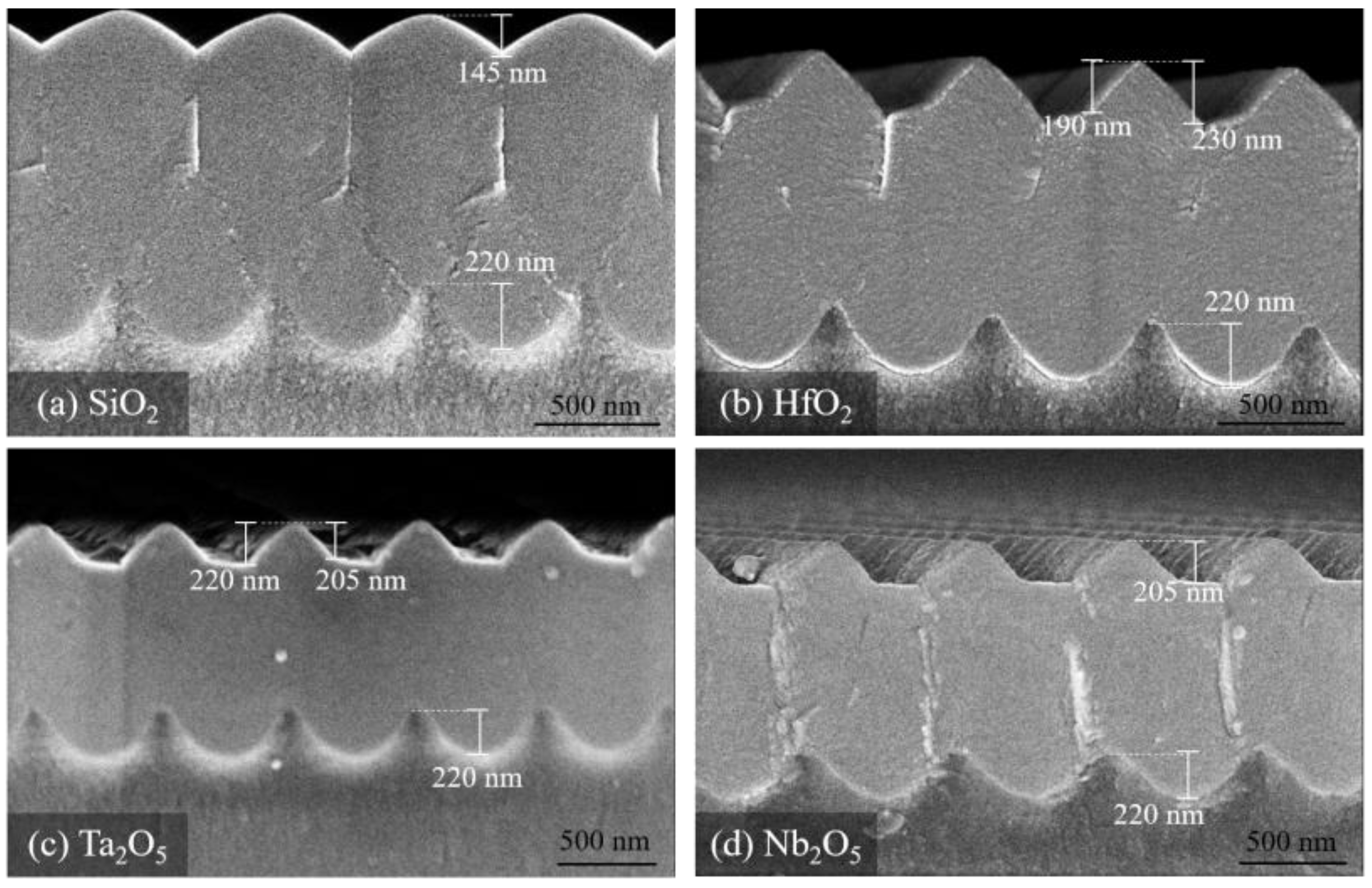
3.2. Structural Analysis of IBS Single-Layer Coatings

To evaluate the conformality of IBS coatings, single-layer films of various dielectric materials—high refractive index (HfO2, Ta2O5, and Nb2O5) and low refractive index (SiO2)—with thicknesses around 1 µm were deposited on structured surfaces. Surface morphology and geometry were characterized by an atomic force microscope (Figure 4) and cross-sectional SEM imaging (Figure 5). Modulation depth analysis revealed reductions of 4.5% for HfO2, 3.2% for Ta2O5, and 10% for Nb2O5, with the most significant decrease (35%) observed for the SiO2 layer. Moreover, high-refractive-index materials maintained a triangular modulation profile, whereas SiO2 exhibited a more rounded morphology.
Since the deposition parameters were based on standard optical coating deposition processes, we further examined the impact of oxygen flow rate on film conformality. As shown in Table 1, the oxygen flow for hafnium oxide deposition is significantly lower than that for other metal oxide films. To determine its effect on coating properties, HfO2 single-layer films were produced using both 5 sccm and 80 sccm of oxygen. Cross-sectional SEM images (Figure 6a,b) indicate that with 5 sccm of O2, the modulation depth decreased by 4.5%, whereas under oxygen-rich conditions (80 sccm), the reduction was 8.1%.
Additionally, optical properties of HfO2 films deposited on flat fused-silica substrates were evaluated. As illustrated in Figure 6c,d, the refractive index at a wavelength of 900 nm decreased from 2.02 with 5 sccm O2 to 1.93 with 80 sccm O2, accompanied by significantly increased optical losses. These results suggest that while oxygen flux influences optical characteristics, it has minimal impact on film conformality.
The more rapid modulation flattening observed with the SiO2 film is likely attributed to its intrinsic chemical properties. Table 2 compares the molecular weights of the pure materials used in depositions. Pure materials are analyzed rather than their oxides since the sputtered atoms are oxidized upon reaching the substrate. Hafnium and tantalum, with higher molecular weights than silicon or niobium, are less easily scattered by residual gas, resulting in denser films and slower modulation smoothening.

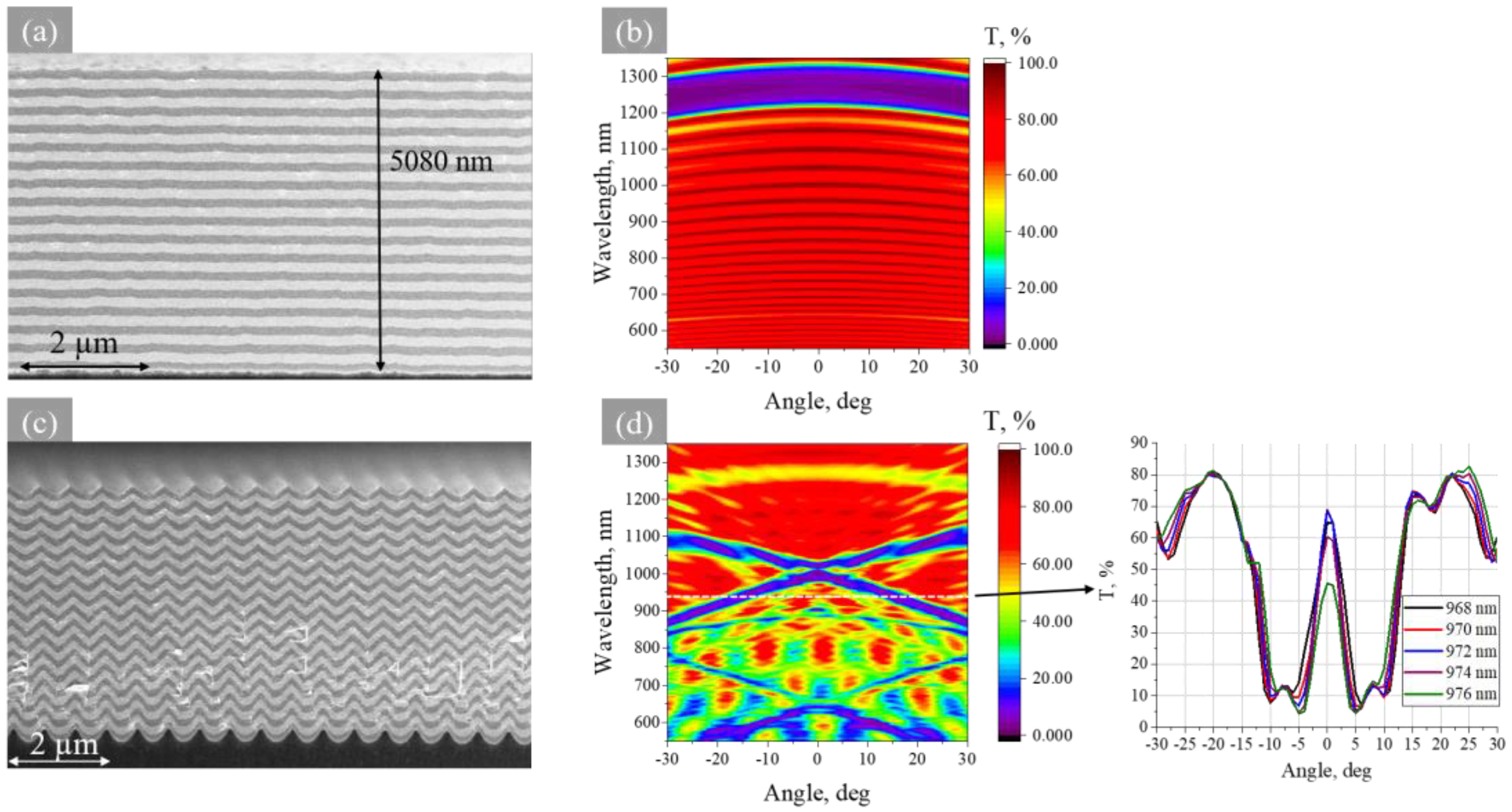
3.3. Optical Analysis

Notably, both single-layer and multilayer coatings produced on periodically modulated surfaces are of high interest to the laser community as such structures can provide unique characteristics such as spatial filtering. The spatial filtering effect in nanostructured single-layer coatings arises from Fano-type resonances caused by the excitation of waveguide modes in the film and is explained in detail here [11]. Filtering in nanostructured multilayer coatings can be attributed to photonic bandgaps and has more freedom in the optimization of the electric field distribution, optical characteristics, etc.
The main difference in multilayer coating deposited on a planar surface or periodically modulated surface is that in the latter case there is an additional level of design complexity. One can reach the periodic distribution of the refractive index not in one dimension, as in standard interference coatings, but in two or three dimensions depending on the substrate. Periodicity initiated from the substrate allows us to reach conditions to excite waveguiding modes, which interact with Fabry–Perot modes and can create additional, different-shape, high-reflectance/high-transmittance zones in transmittance maps.
Multilayer coatings based on alternating HfO2 and Nb2O5 layers deposited on planar and modulated surfaces are shown as an example of optical response complexity (see Figure 7). The total number of 33 layers deposited on the planar surface serves as an interference coating (Bragg mirror) with one prominent high-reflection zone for 1250 nm wavelength. The same coating (the same deposition run) fabricated on a substrate with a 600 nm periodic surface modulation can lead to different shapes and positions of high-reflectance zones in transmittance maps. Such resonant “crosses” in transmittance maps allow spatial filters for particular wavelengths to be formed, as the light incident at zero angle is highly transmitted, while light incident at higher angles is reflected. The theoretical analysis and application of such multilayer structures were analyzed in our group’s previous work [12].

4. Conclusions

A series of experiments were conducted to evaluate various thin film deposition techniques for the replication of modulated submicron surfaces. Few micron-thickness multilayer coatings were deposited using electron beam evaporation with glancing angle deposition and plasma assistance, atomic layer deposition, and ion beam sputtering techniques, and their surface geometries were characterized. Coatings produced via electron beam evaporation with glancing angle deposition rapidly smoothed the surface modulation due to the low kinetic energy of evaporated atoms. Similar results were obtained with plasma-assisted deposition using continuous sample rotation, whereas ion-assisted deposition with the substrate maintained in a stationary position above the plasma source provided highly replicated coatings but introduced substrate damage. Although atomic layer deposition can produce conformal thin films, thick coatings exhibit significant surface smoothing and can cause substrate cleavage due to high internal stress.
In our experiments, ion beam sputtering has proven to be the most promising technique for producing dense and replicating multilayer coatings on corrugated substrates while maintaining a significant fraction of the initial modulation. Additionally, we demonstrated the difference in surface replication for different single-layer coatings deposited by ion beam sputtering. High-refractive-index materials (Ta2O5, HfO2, and Nb2O5) provided higher replication with modulation reductions by 3.2%, 4.5%, and 10%, respectively, compared to a 35% reduction observed for the SiO2 single-layer coating. Moreover, high-refractive-index structured coatings and multilayer structured coatings can be used as spectral and spatial filtering elements in various laser or photonics systems.

Author Contributions

Conceptualization, supervision, analysis—L.G.; Ebeam and IBS coating fabrication—L.G., J.N. and S.M.; ALD coating fabrication—M.D. and D.A.; AFM and spectrophotometric measurements—L.G. and J.N.; SEM images—A.S.; Writing—original draft—L.G. and D.A. All authors have read and agreed to the published version of the manuscript.

Funding

This work was supported by the PerFIN project from the Research Council of Lithuania (LMTLT), agreement No. S-MIP-22–80. Also, from Horizon 2020 ERA.NET-COFUND program project MiLaCo (Project No. S-M-ERA.NET-20-2).

Institutional Review Board Statement

Not applicable.

Informed Consent Statement

Not applicable.

Data Availability Statement

Dataset available on request from the authors.

Acknowledgments

We thank Geola Ltd. (Lithuania) for providing plates with photoresist film and D. Gailevičius from Vilnius University (Lithuania) for the soft nanoimprint lithography process to fabricate copies of the master grating structure.

Conflicts of Interest

The authors declare no conflicts of interest.

References

  1. Wang, P.Y.; Herrero, R.; Botey, M.; Cheng, Y.C.; Staliunas, K. Translationally Invariant Metamirrors for Spatial Filtering of Light Beams. Phys. Rev. A 2020, 102, 013517. [Google Scholar] [CrossRef]
  2. Lymarenko, R.A.; Gailevicius, D.; Meskelaite, I.; Grineviciute, L.; Peckus, M.; Staliunas, K.; Taranenko, V.B. Super-Collimation by Axisymmetric Diffractive Metamirror. Opt. Lett. 2021, 46, 3845. [Google Scholar] [CrossRef] [PubMed]
  3. Grinevičiūtė, L.; Andrulevičius, M.; Melninkaitis, A.; Buzelis, R.; Selskis, A.; Lazauskas, A.; Tolenis, T. Highly Resistant Zero-Order Waveplates Based on All-Silica Multilayer Coatings. Phys. Status Solidi 2017, 214, 1700764. [Google Scholar] [CrossRef]
  4. Mireles, M.; Hoffman, B.N.; MacNally, S.; Smith, C.C.; Lakshmanan, S.N.; Lambropoulos, J.C.; Rigatti, A.L.; Demos, S.G. Direct-Write Laser-Assisted Patterning of Form Birefringence in Wave Plates Fabricated by Glancing-Angle Deposition. Optica 2023, 10, 657. [Google Scholar] [CrossRef]
  5. Plukys, M.; Grineviciute, L.; Nikitina, J.; Gailevicius, D.; Staliunas, K. Enhancement of Brightness in Microchip Laser with Angular Filtering Mirrors. Opt. Laser Technol. 2025, 181, 111904. [Google Scholar] [CrossRef]
  6. Doucet, A.; Beydaghyan, G.; Ashrit, P.V.; Bisson, J.-F. Compact Linearly Polarized Ceramic Laser Made with Anisotropic Nanostructured Thin Films. Appl. Opt. 2015, 54, 8326. [Google Scholar] [CrossRef]
  7. Liu, R.; Cao, L.; Liu, D.; Wang, L.; Saeed, S.; Wang, Z. Laser Interference Lithography—A Method for the Fabrication of Controlled Periodic Structures. Nanomaterials 2023, 13, 1818. [Google Scholar] [CrossRef]
  8. Sebastian, E.M.; Jain, S.K.; Purohit, R.; Dhakad, S.K.; Rana, R.S. Nanolithography and Its Current Advancements. Mater. Today Proc. 2020, 26, 2351–2356. [Google Scholar] [CrossRef]
  9. Mehta, A.; Brown, J.D.; Srinivasan, P.; Rumpf, R.C.; Johnson, E.G. Spatially Polarizing Autocloned Elements. Opt. Lett. 2007, 32, 1935. [Google Scholar] [CrossRef]
  10. Sergeant, N.P.; Agrawal, M.; Peumans, P. High Performance Solar-Selective Absorbers Using Coated Sub-Wavelength Gratings. Opt. Express 2010, 18, 5525. [Google Scholar] [CrossRef]
  11. Grineviciute, L.; Nikitina, J.; Babayigit, C.; Staliunas, K. Fano-like Resonances in Nanostructured Thin Films for Spatial Filtering. Appl. Phys. Lett. 2021, 118, 131114. [Google Scholar] [CrossRef]
  12. Grineviciute, L.; Babayigit, C.; Gailevičius, D.; Peckus, M.; Turduev, M.; Tolenis, T.; Vengris, M.; Kurt, H.; Staliunas, K. Nanostructured Multilayer Coatings for Spatial Filtering. Adv. Opt. Mater. 2021, 9, 2001730. [Google Scholar] [CrossRef]
  13. Balonek, G. Coating a Grating Structure Using Various Deposition Techniques; University of Rochester, Institute of Optics: Rochester, NY, USA, 2013. [Google Scholar]
  14. Oliver, J.B.; Kessler, T.J.; Charles, B.; Smith, C. LLE Review; Quarterly Report; DOE/NA/1944-1170; University of Rochester, Laboratory for Laser Energetics: Springfield, VA, UAS, 2014; Volume 138, pp. 148–151. [Google Scholar]
  15. Oliver, J.B.; Kessler, T.J.; Charles, B.; Smith, C. Fabrication of a Continuous-Enfolded Grating by Ion-Beam–Sputter Deposition; SVC Techcon: Nashville, TN, USA, 2015; pp. 483–487. [Google Scholar]
  16. Yakovlev, N.N.; Almaev, A.V.; Kushnarev, B.O.; Verkholetov, M.G.; Poliakov, M.V.; Zinovev, M.M. β-Ga2O3 Schottky Barrier Diode with Ion Beam Sputter-Deposited Semi-Insulating Layer. Crystals 2024, 14, 123. [Google Scholar] [CrossRef]
  17. Henn, S.; Dornberg, G.; Müller, A.; Bundesmann, C.; Frost, F.; Sturm, C.; Grundmann, M. Optical and Structural Characterization of Zinc Oxide Thin Films upon Ion Beam Assisted Smoothing. Thin Solid Film. 2024, 794, 140290. [Google Scholar] [CrossRef]
  18. Kalanov, D.; Gerlach, J.W.; Bundesmann, C.; Bauer, J.; Lotnyk, A.; Von Wenckstern, H.; Anders, A.; Unutulmazsoy, Y. Heteroepitaxial Growth of Ga2O3 Thin Films on Al2O3(0001) by Ion Beam Sputter Deposition. J. Appl. Phys. 2024, 136, 015302. [Google Scholar] [CrossRef]
  19. Kawashima, T. Autocloning Technology: Fabrication Method for Photonic Crystals Based on Sputtering Process. In Proceedings of the AIP Conference Proceedings, Baltimore, MD, USA, 4–6 April 2001; AIP: Erice, Italy, 2001; Volume 560, pp. 115–122. [Google Scholar]
  20. Srinivasan, P. Design and Fabrication of Space Variant Micro Optical Elements. Master’s Thesis, University of Central Florida, Orlando, FL, USA.
  21. Ohtera, Y.; Onuki, T.; Inoue, Y.; Kawakami, S. Multichannel Photonic Crystal Wavelength Filter Array for Near-Infrared Wavelengths. J. Light. Technol. 2007, 25, 499–503. [Google Scholar] [CrossRef]
  22. Destouches, N.; Pommier, J.-C.; Parriaux, O.; Clausnitzer, T.; Lyndin, N.; Tonchev, S. Narrow Band Resonant Grating of 100% Reflection under Normal Incidence. Opt. Express 2006, 14, 12613. [Google Scholar] [CrossRef]
  23. Chen, S.-H.; Chen, C.-K.; Huang, Y.-C.; Lee, C.-C. Omni-Directional Reflectors for Deep Blue LED Using Symmetric Autocloning Method. Opt. Rev. 2013, 20, 141–144. [Google Scholar] [CrossRef]
  24. George, S.M. Atomic Layer Deposition: An Overview. Chem. Rev. 2010, 110, 111–131. [Google Scholar] [CrossRef]
  25. Pinna, N.; Knez, M. (Eds.) Atomic Layer Deposition of Nanostructured Materials, 1st ed.; Wiley: Hoboken, NJ, USA, 2011; ISBN 978-3-527-32797-3. [Google Scholar]
  26. Cremers, V.; Puurunen, R.L.; Dendooven, J. Conformality in Atomic Layer Deposition: Current Status Overview of Analysis and Modelling. Appl. Phys. Rev. 2019, 6, 021302. [Google Scholar] [CrossRef]
  27. Astrauskytė, D.; Galvanauskas, K.; Gailevičius, D.; Drazdys, M.; Malinauskas, M.; Grineviciute, L. Anti-Reflective Coatings Produced via Atomic Layer Deposition for Hybrid Polymer 3D Micro-Optics. Nanomaterials 2023, 13, 2281. [Google Scholar] [CrossRef] [PubMed]
  28. Bhattacharya, R.S.; Rai, A.K.; McCormick, A.W. Ion-Beam-Assisted Deposition of Al2O3 Thin Films. Surf. Coat. Technol. 1991, 46, 155–163. [Google Scholar] [CrossRef]
  29. RF Plasma Source, CCR GmbH. Available online: https://www.rf-icp-plasmasources.com/copra-products/copra-built-in-sources/copra-built-in-plasma-sources (accessed on 21 March 2025).
  30. Abromavičius, G.; Juodagalvis, T.; Buzelis, R.; Juškevičius, K.; Drazdys, R.; Kičas, S. Oxygen Plasma Etching of Fused Silica Substrates for High Power Laser Optics. Appl. Surf. Sci. 2018, 453, 477–481. [Google Scholar] [CrossRef]
  31. CEC GmbH. Operation Manual Deposition System “IBS@LAB”; Cutting Edge Coatings GmbH: Hannover, Germany, 2009. [Google Scholar]
  32. Abromavičius, G. Microstructural and Optical Properties of Metal Oxide Optical Coatings Deposited by Ion Beam Sputtering and Their Application in UV Spectral Range. Ph.D. Thesis, Vilniaus Universitetas, Vilnius, Lithuania, 2020. [Google Scholar]
  33. Kaufman, H. Applications of Broad-Beam Ion Sources; Kaufman & Robinson, Inc.: Fort Collins, CO, USA, 2011. [Google Scholar]
  34. Stenzel, O. Optical Coatings: Material Aspects in Theory and Practice; Springer Series in Surface Sciences; Springer: Berlin/Heidelberg, Germany, 2014; Volume 54, ISBN 978-3-642-54062-2. [Google Scholar]
  35. Çetinörgü-Goldenberg, E.; Klemberg-Sapieha, J.-E.; Martinu, L. Effect of Postdeposition Annealing on the Structure, Composition, and the Mechanical and Optical Characteristics of Niobium and Tantalum Oxide Films. Appl. Opt. 2012, 51, 6498. [Google Scholar] [CrossRef] [PubMed]
  36. Gabriel, N.T.; Talghader, J.J. Thermal Conductivity and Refractive Index of Hafnia-Alumina Nanolaminates. J. Appl. Phys. 2011, 110, 043526. [Google Scholar] [CrossRef]
  37. Gieraltowska, S.; Wachnicki, L.; Dluzewski, P.; Witkowski, B.S.; Godlewski, M.; Guziewicz, E. Atomic Layer Deposition of HfO2 Films Using TDMAH and Water or Ammonia Water. Materials 2023, 16, 4077. [Google Scholar] [CrossRef] [PubMed]
  38. Groner, M.D.; Fabreguette, F.H.; Elam, J.W.; George, S.M. Low-Temperature Al2O3 Atomic Layer Deposition. Chem. Mater. 2004, 16, 639–645. [Google Scholar] [CrossRef]
  39. Myers, T.J.; Throckmorton, J.A.; Borrelli, R.A.; O’Sullivan, M.; Hatwar, T.; George, S.M. Smoothing Surface Roughness Using Al2O3 Atomic Layer Deposition. Appl. Surf. Sci. 2021, 569, 150878. [Google Scholar] [CrossRef]
  40. Gerritsen, S.H.; Chittock, N.J.; Vandalon, V.; Verheijen, M.A.; Knoops, H.C.M.; Kessels, W.M.M.; Mackus, A.J.M. Surface Smoothing by Atomic Layer Deposition and Etching for the Fabrication of Nanodevices. ACS Appl. Nano Mater. 2022, 5, 18116–18126. [Google Scholar] [CrossRef]
  41. Lau, W.S.; Du, L.; Yu, D.Q.; Wang, X.; Wong, H.; Xu, Y. The Application of a Selective Etch to Conclusively Show the Surface Smoothing Effect of an Amorphous Thin Film Deposited by Atomic Layer Deposition. ECS J. Solid State Sci. Technol. 2017, 6, N111–N116. [Google Scholar] [CrossRef]
  42. Lau, W.S.; Zhang, J.; Wan, X.; Luo, J.K.; Xu, Y.; Wong, H. Surface Smoothing Effect of an Amorphous Thin Film Deposited by Atomic Layer Deposition on a Surface with Nano-Sized Roughness. AIP Adv. 2014, 4, 027120. [Google Scholar] [CrossRef]
  43. PubChem—An Open Chemistry Database at the National Institutes of Health (NIH). Available online: https://Pubchem.Ncbi.Nlm.Nih.Gov/#query=niobium (accessed on 21 March 2025).
Figure 1. (a) The schematic of a laser setup and (b) a real laser setup for the interference lithography process (blue arrows represent the path of laser beam).
Coatings 15 00372 g001
Figure 2. Measured results of fabricated gratings: (a) the depth of the grating modulation dependency on the development time in KOH solution. (b) AFM measurements of the typical grating surface; (c) the transmittance map (transmission depending on the angle (horizontal axis) and wavelength (vertical axis)).
Coatings 15 00372 g002
Figure 3. The deposition of multilayer coatings on a patterned substrate using different technologies: (a) e-beam evaporation with glancing angle deposition method, SiO2 dense and porous layers (red dashed line marks the interface between the substrate and the coating), (b) e-beam evaporation with plasma source while the substrate rotates in the calotte, Al2O3 and SiO2 multilayer (c) e-beam evaporation with plasma source while the substrate is stationary above the plasma flux, Al2O3 and SiO2 multilayer. (d) Atomic layer deposition, Al2O3 and HfO2 multilayer. (e) Ion beam sputtering, Ta2O5 and SiO2 multilayer.
Coatings 15 00372 g003
Figure 4. AFM measurements of single-layer surfaces fabricated from different materials: (a) SiO2, (b) HfO2, (c) Ta2O5, and (d) Nb2O5.
Coatings 15 00372 g004
Figure 5. SEM images of cross-sections of fabricated single layers from different materials: (a) SiO2, (b) HfO2, (c) Ta2O5, and (d) Nb2O5 materials.
Coatings 15 00372 g005
Figure 6. SEM images of cross-sections of the fabricated samples of HfO2 material by using different amounts of oxygen during the deposition process: (a) 5 sccm and (b) 80 sccm. (c) Refractive index and (d) extinction coefficient dispersions of HfO2 layers fabricated using different flow rates of O2 during the deposition process.
Coatings 15 00372 g006
Figure 7. The structural and optical comparison of multilayer coating deposited on planar and patterned surface. SEM images with corresponding transmittance maps of the same HfO2-Nb2O5 multilayer structure deposited on (a,b) flat surface, and on (c,d) a periodically modulated surface.
Coatings 15 00372 g007
Table 1. The summarized IBS reactive process parameters for the formation of HfO2, Ta2O5, Nb2O5, and SiO2 single-layer coatings.
MaterialRefractive Index at
λ = 980 nm
O2 Flux, sccmPartial Pressure, mbarPhysical Thickness, nm
HfO22.0155.0·10−51000
HfO21.94801.4·10−41000
SiO21.48801.4·10−41000
NbO22.24801.4·10−41000
Ta2O52.09408.0·10−5900
Table 2. The molecular weight and density of different materials [43].
MaterialMolecular Weight, g/mol
Si28.09
Hf178.49
Ta180.95
Nb92.90
Disclaimer/Publisher’s Note: The statements, opinions and data contained in all publications are solely those of the individual author(s) and contributor(s) and not of MDPI and/or the editor(s). MDPI and/or the editor(s) disclaim responsibility for any injury to people or property resulting from any ideas, methods, instructions or products referred to in the content.

