1. Introduction
Diamond-like carbon (DLC) has for many years been a material with high promise [
1]. Only recently, industrial applications of DLC and thin film technology have successfully replaced traditional functional coatings such as TiN in cutting machinery [
2,
3]. Newly tailored carbon materials appear in novel appliances, e.g. in ultra-capacitors [
4]. An overview of the history of DLC coatings has been recently presented [
5]. DLC’s excellent mechanical properties and chemical inertness enables use in applications as diverse as functional coatings in bio-medical implants to inner wall pipelines [
6]. Ion implantation has been shown to functionalise the DLC coating [
7]. The properties of the coatings are strongly dependent on their structure [
8,
9]. Amongst a large number of analysis techniques that are available for investigating structural properties, Raman spectroscopy is often used as a first tool to accurately determine the sp
3/sp
2 ratio in the DLC coatings, which is important to determine the hardness and wear resistance of the coatings [
10]. Additional analysis techniques are nano-indentation, friction measurements, electron microscopy, and stoichiometry measurements [
1,
2,
5,
9].
Different fabrication methods can be used to produce DLC coatings with varying properties [
5,
11]. It is possible to tailor the DLC coating process to achieve, e.g., very hard coatings with high sp
3 content or low-friction coatings with high sp
2 content [
5,
12,
13]. While the sp
3 hybridisation ensures strong bonding in all three dimensions, sp
2 hybridisation causes strong s-bonds in the plane and weak van der Waals forces perpendicular to the plane resulting in an anti-seizing agent becoming the material of choice for “lubricant” between moving parts [
1,
5]. As described in [
6], each method has its merits.
At GNS Science, we have developed a novel anode layer ion source that is depositing DLC under 360° simultaneously to coat the inside of a pipe. The arrangement makes use of a cradle to move the ion source along, inside the pipe and does not require any other moving parts [
6,
14]. The ion source produces micrometre thick DLC coatings simply by pulling the source along the centre of the pipe at a constant speed. Raman spectroscopy has been used to probe for the disorder in the coatings (
ID/
IG ratio, full width half maximum of
Gpeak (G-FWHM)), which is an indicator for the hardness of the coating. The coatings produced by the circular anode layer ion source have a G-FWHM of 160–170 indicating a hardness of >20 GPa considering data published in [
6,
15]. Atomic force microscope (AFM) measurements revealed a surface roughness of less than 50 nm indicating low friction supported by a C/H ratio of 3:1 measured with Rutherford backscattering spectrometry [
6].
Following the study of the ID/IG ratio, hardness and surface morphology of the DLC coatings produced with the novel ion source, the aim of this publication is to determine the structure and growth of the coatings in the 4–8 kV acceleration voltage range. Based on the results obtained from cross-sectional transmission electron microscopy (X-TEM) and energy dispersive X-ray (EDX) analyses, a growth model is proposed for the DLC deposition using the CALIS ion source.
2. Methods
The samples were fabricated with a circular anode layer ion source (CALIS) [
6,
14]. Butane was used as a precursor gas. Major advantages of the system are the use of non-rotating parts, simplicity of electronics and ability to coat any conductive material that is presented to the ion beam, which even extends to some degree to insulating materials. The electronics required to produce the ion beam consists of a single high voltage power supply to generate a potential difference between the anode and cathode in the source and to accelerate the ions onto the targets. Permanent magnets are used in the source to generate the magnetic confinement field [
6,
14].
For the experiments, the anode voltage was set at 1.5 kV. The total acceleration voltage was adjusted between 4 and 8 kV to create a strong bonding between the coating and the substrate at the interface. The output current was set to 10 mA by adjusting the operational pressure (10
−5 hPa range). CALIS deposits DLC coatings simultaneously in 360° geometry [
6,
14]. The experimental set-up of the ion source is designed to produce DLC coatings on the inside of a 150 mm stainless steel pipe. Silicon <100> was used as substrate material. The CALIS source was typically moved, along the pipe centre with a speed of 1.5 mm h
−1 across the substrates to produce laterally homogenous coatings over long distances.
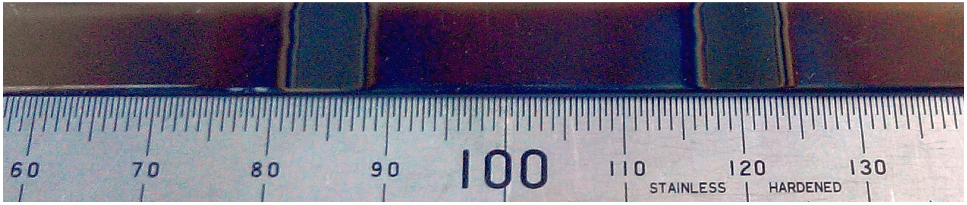
Figure 1 shows two representative sections of tracks of DLC coatings on stainless steel produced in two stages. The first coating was produced with 6 keV acceleration voltage to produce a track centred at about 84 mm. The second track centred around 120.5 mm was produced with an acceleration voltage of 8 keV. Both coatings were produced with an ion current of 10 mA. The second ion track was produced after the ion source was moved by ~35 mm. The coatings are silver in colour and about 5 mm wide. The 4 µm approximately thick coatings stick very well to the stainless steel substrate that was placed inside of the pipe. The steel substrates were neither physically nor chemically cleaned prior to the deposition process to present a surface to the ion source that is similar to an untreated pipe wall.
Figure 1.
Representative diamond-like carbon (DLC) coatings on stainless steel.
Figure 1.
Representative diamond-like carbon (DLC) coatings on stainless steel.
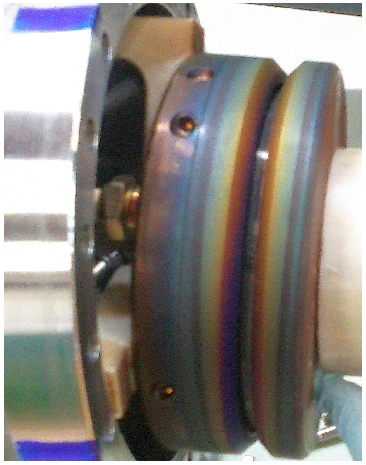
Figure 2 shows an image of the ion source while it is loaded into a 150 mm pipe for testing purposes. A schematic drawing of the ions source set-up is shown in [
6].
As can be seen, the ion source has radial geometry, electrical and gas feedthroughs on the left hand side and a holding mechanism on the right hand side for the carriage system, which moves the ion source inside of the pipe. The cathode gap of this particular ion source is set to 2 mm. The colour of the ion source surface close to the cathode gap indicates that thin DLC films that have been deposited during the coating process. The system is currently limited to a minimum acceleration voltage of 1500 V due to the requirement of an anode potential of 1500 V in this geometry and to a maximum acceleration voltage of 20 kV due to the combination of operating gas pressure in the pipe of 10−5 hPa and the distance of the source from the inner wall of 5 mm. The source has been manufactured for a pipe with 150 mm diameter. In principle, the ion source can be manufactured to fit in pipes of about 25 mm to more than 300 mm depending on the application.
A stationary ion source-substrate configuration was used additionally to investigate the beam spread of the ion source. Profilometry is a common method to determine the thickness of the coating [
16]. A SLOAN Dektak Profilometer was used with scanning speeds of 1 to 10 mm min
−1. The height accuracy was measured to be ±10 nm. Line scans across areas of interest revealed the height profiles.
Figure 2.
Image of the radial ion source during a loading process.
Figure 2.
Image of the radial ion source during a loading process.
Cross-sections of the samples were analysed with an image-corrected Titan 80–300 microscope (FEI, Hillsboro, OR, USA) characterized by a point resolution of 0.1 nm. The samples were prepared with a focused ion beam system (FIB) to produce lamellae that were sufficiently thin for the TEM analysis. A Ga+ ion beam was used to make two precise wedged trenches in the sample to produce a thin standing wall lamella which was handled by a micro-manipulator. This is an optimum method to investigate specific regions of interest within a sample. However, this method can leave traces of heavy ions on the cross sections (e.g., Ga implanted into or Pt from the protection layer smeared across the side walls of the lamella) as well as marks from the cutting process. Each lamella was welded onto a TEM grid to support the cross-sectional structure during microscopy. Energy dispersive X-ray spectroscopy (EDX, FEI, Hillsboro, OR, USA) was used to study the elemental composition of the coatings by measuring the characteristic X-ray energy of major, minor and trace elements with an estimated lateral resolution of a few nm in the present case.
3. Results and Discussion
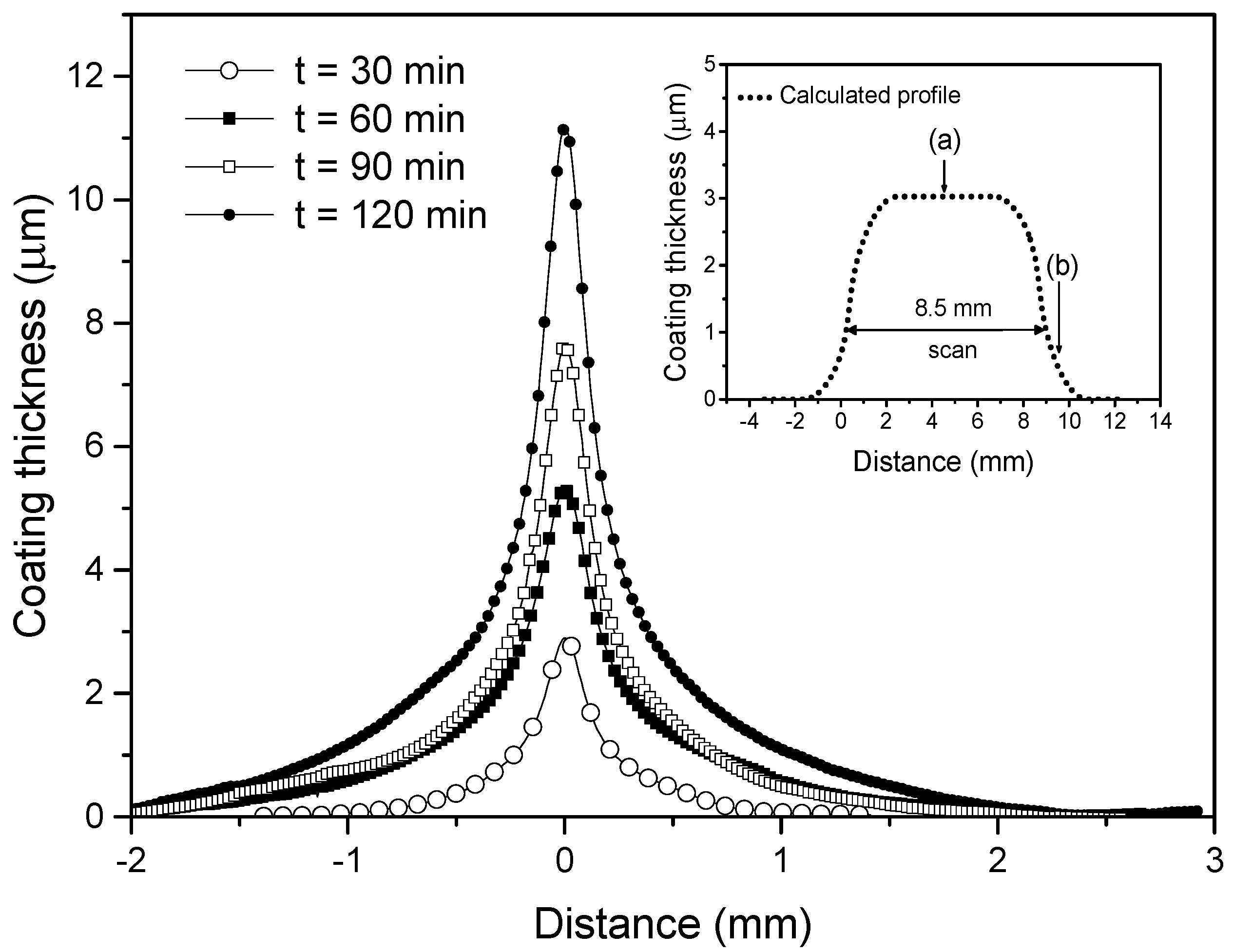
Figure 3 shows measured deposition profiles of DLC coatings on silicon prepared with an acceleration voltage of 6 kV, an anode current of 10 mA and deposition times of 30, 60, 90 and 120 min. These profiles were obtained with stationary source-substrate configurations. The deposition profiles are geometrically bound to this ion source configuration with a central region that coats the substrate perpendicular to the surface and with run out regions to each side of the central beam. Run out regions refer to the coatings produced under non perpendicular ion beam deposition. In particular, it refers to those regions that are exposed to the less intense area of the beam spread or to the ion beam scattered from the source components. As can be seen in
Figure 3, the ion beam from the source is strongly focused in a narrow region. The face of the source was positioned 5 mm away from the silicon substrates. The deposition rate was calculated to be 65 ± 5 nm min
−1 for the narrow region. As it can be expected from the geometry of the ion source [
6,
14], the deposition profile of the DLC coating peaks in the centre and has a wide tail region to both sides. A Lorentz fit describes the peak function well with reduced chi
2 or chi
2 divided by the degrees of freedom (DoF) where DoF = 0.029 for the coating deposited for 120 min. The explained variation divided by the total variation is
R2 = 0.994. This function has a half width half maximum of
w = 0.236. The deposition rate is time independent within production and measuring errors. The set-up allows the ion source to travel over the substrates at a speed of 1.5 mm h
−1. This results in DLC coatings with a similar thickness across large regions. Typically, 3 µm thick DLC coatings are produced using the parameters as described above and is indicated by the dotted line in
Figure 3 that considers a travel distance of the ion source of 8.5 mm. The arrows in the figure indicate the plateau region (a) as well as the run out region (b).
Figure 3.
Representative time dependent DLC deposition profiles produced with a stationary ion source. The inset represents the calculated profile of a DLC deposition with a moving ion source. Plateau (a) and run off regions (b) are indicated.
Figure 3.
Representative time dependent DLC deposition profiles produced with a stationary ion source. The inset represents the calculated profile of a DLC deposition with a moving ion source. Plateau (a) and run off regions (b) are indicated.
Samples deposited at 4, 6 and 8 kV acceleration voltage were analysed with cross-sectional TEM. Results are presented in
Figure 4,
Figure 5,
Figure 6 and
Figure 7.
Figure 4 and
Figure 5 show cross-sectional images taken in the plateau regions (
Figure 3a),
Figure 6 shows an EDX analysis and
Figure 7 shows a cross-sectional image from the run out region (
Figure 3b).
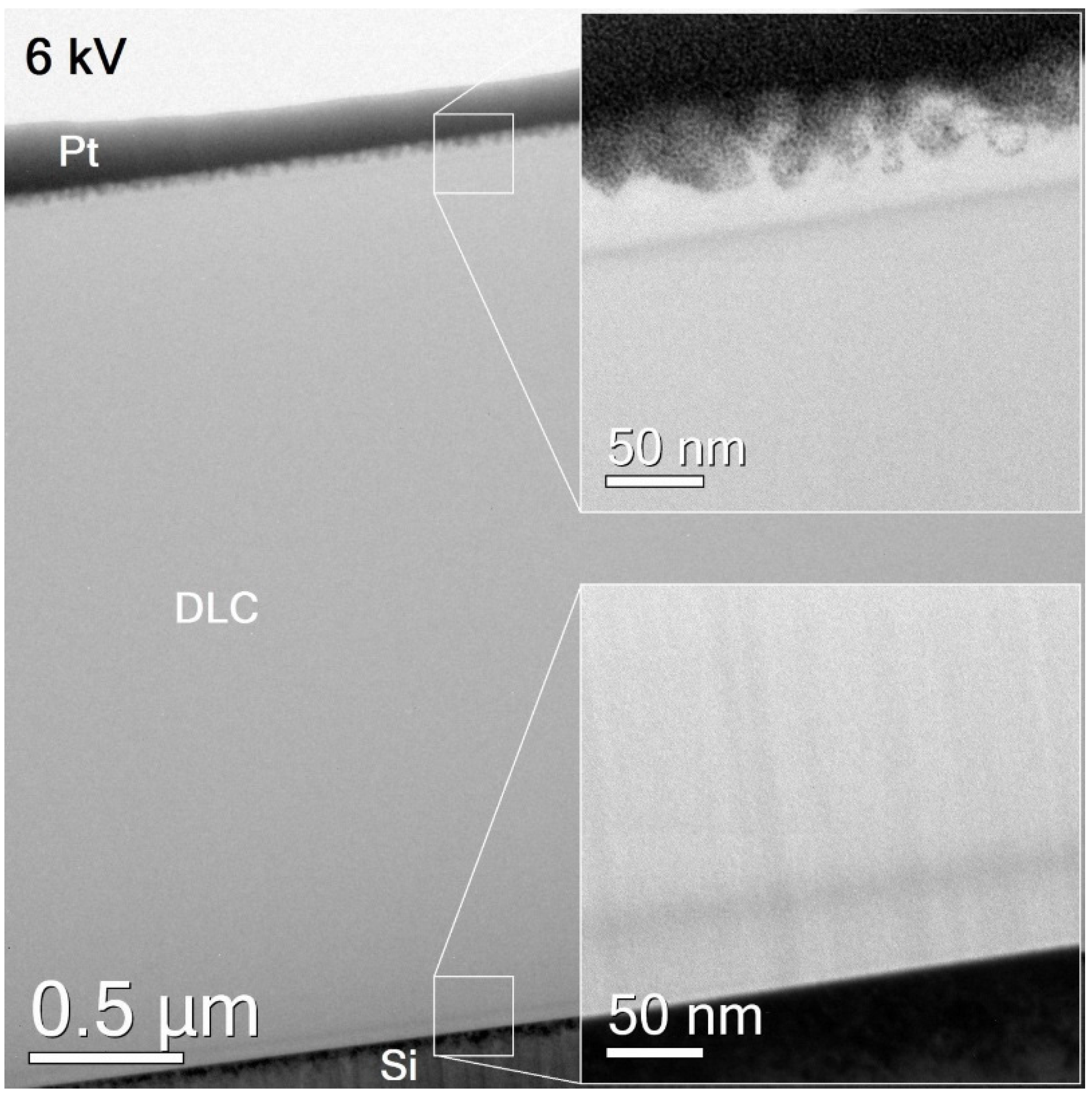
Figure 4 and
Figure 5 show that the coatings have similar thickness of about 3µm in the plateau region and a distinct three-layered structure. The first layer is visible in the TEM image at the Si-DLC coating interface. The magnified image shows a clearly noticeable dark region in the coating about 50 nm above the Si substrate. The second layer represents the “standard” amorphous DLC coating. The third layer is a fringed disordered top layer covered with Pt from the TEM sample preparation process. Noticeably, the top layer is darker grey in contrast compared to the middle layer which may be due to some short range ordering and/or the presence of heavy elements causing the variation in contrast. This is supported by results described later in the paper. Cutting marks from the FIB lamella sample preparation process are visible in the images in
Figure 4 and
Figure 5 as dark lines, in particular in the coating region close to the Si substrate.
Figure 4.
Cross-sectional TEM image of a DLC coating on silicon produced with an acceleration voltage of 8 kV. Insets show magnified regions at the interfaces.
Figure 4.
Cross-sectional TEM image of a DLC coating on silicon produced with an acceleration voltage of 8 kV. Insets show magnified regions at the interfaces.
Figure 5.
Cross-sectional TEM image of a DLC coating on silicon produced with an acceleration voltage of 6 kV. Insets show magnified regions at the interfaces.
Figure 5.
Cross-sectional TEM image of a DLC coating on silicon produced with an acceleration voltage of 6 kV. Insets show magnified regions at the interfaces.
Figure 6.
Energy dispersive X-ray spectra of a DLC coating prepared with 8 kV in the interface regions at the substrate (a) and the surface (b).
Figure 6.
Energy dispersive X-ray spectra of a DLC coating prepared with 8 kV in the interface regions at the substrate (a) and the surface (b).
Figure 7.
Cross-sectional TEM analysis of a DLC coating produced with 4 kV in region (b) referring to
Figure 3. Magnified insets of the interfaces are shown along with a Fourier transformation of the boxed area in the lower right inset.
Figure 7.
Cross-sectional TEM analysis of a DLC coating produced with 4 kV in region (b) referring to
Figure 3. Magnified insets of the interfaces are shown along with a Fourier transformation of the boxed area in the lower right inset.
EDX analyses of the coating prepared with an acceleration voltage of 8 kV, covering the regions from the surface and interface, are shown in
Figure 6. This analysis provides insights into the three-layered structure.
Figure 6a shows the results of the EDX measurements recorded in the DLC/Si interface region. The measurements were performed at six distinct areas across the transition region from the substrate to the amorphous DLC coating. The following elements were detected: C, Si, Ga, Cu, Fe, Cr, Cl and S. The Ga signal is visible throughout the EDX measurements and originates from the FIB lamella sample preparation process. The Cu peaks observed equally throughout the EDX measurements are mainly from fluorescence excitation of the TEM grid. Area 1 in
Figure 6a shows only a Si signal from the substrate. Other elements are not detected. Areas 2–4 show Fe and Cr in the coating. These elements are absent in the middle region of the coating (e.g., areas 5 and 6).
Figure 6b shows EDX measurements performed near the surface of the coating and across the transition of the amorphous DLC coating to the Pt cover layer. The results of the EDX analysis are similar to that of the interface. Area 1, being in the amorphous DLC coating region shows insignificant signals from Fe, Cr, and Cl, whereas these elements are present in larger amounts in areas 2–4. Additionally, Pt of the cover layer is measured in area 4. Silicon is interestingly measured throughout the coating with gradually decreasing concentration from the interface at the substrate to the surface. Although this Si signal can be explained by the fluorescence of X-rays from the substrate material, a gradual dilution of silicon during the deposition process as suggested by the Robertson’s growth model [
11] cannot be excluded. In summary, the TEM results indicate that the deposition of DLC produced by CALIS in scanned mode is a projection of the deposition profile. The impurity elements Fe, Cr, Cl and S are deposited in the run out areas (
Figure 3b) of the deposition distribution and therefore are measured in both substrate and surface interface layers of the DLC coating. These impurity elements originate from the ion source, pipe and sample mountings. They have increased deposition at non-perpendicular angles of incoming ions due to ion sputtering.
After having analysed the coating structure in the plateau region, the structure of the coating was investigated in the run out region considering that the concentration of the trace elements was found to be different in the interface and surface layers. This may indicate that DLC coatings produced in run out areas have a different structure compared to DLC coatings produced in the plateau region.
Figure 7 shows a cross-sectional TEM image of a DLC coating produced in the run out zone, in particular for the coating fabricated with 4 kV acceleration voltage which has a thickness of 680 nm (refer to
Figure 3b). As for coatings described earlier, the ion current was set to 10 mA. The TEM analysis shows unexpected results for the layer at the interface and surface. Clear structural differences are seen. The interface layer at the substrate displays some porous columnar structures, which are best imaged in out-of-focus condition due to the Fresnel contrast which is based on changes of the inner potential. The lower right inset in the figure shows a magnified image of the DLC/Si interface region recorded in focus condition. Forming a diffractogram by Fourier transformation of the boxed area reveals some hexagonal nanocrystalline structure with a lattice spacing of 150 pm. The coating shown in
Figure 7 was produced about 400 μm away from the start of the coating centre and was therefore not perpendicularly exposed to the ion beam. Both ion current density and temperature development during the deposition process are different to that of the other samples. The differences in the coating structure and the composition when compared to the regions in
Figure 4 and
Figure 5 can thus be attributed to the difference in growth conditions.
The observed three-layered structure is unique to DLC coatings. During ion beam exposure, three types of deposition occur: type (I) initial deposition process that deposits sputtered impurities from the well cleaned ion source that is made from mild steel and contains plastic components internally [
6] along with the incident beam, type (II) perpendicular beam deposition of high current density that builds up an amorphous layer and type (III) a non-perpendicular ion beam deposition of lower current density containing significant amount of impurities sputtered at wide angles from the ion source. When the coating process is initiated, the whole substrate area is covered by type (I) deposition, but with time the source components get coated internally with DLC and the amount of sputtered impurities in the beam incident directly under the source is significantly reduced. This is followed by type (II) deposition. The substrate area under the source is exposed to the highly intense incident ion beam that is responsible for building the thick amorphous middle layer as observed in
Figure 4.
At the same time, the surrounding areas get covered by type (III) deposition which consists of the run out part of the beam spread along with impurities from the source sputtered at wide angles. As the source constantly moves at a speed of 1.5 mm h
−1, the region that was initially under type (II) deposition is covered by type (III) deposition and vice versa. As this process continues, a coating develops that has a sandwich-like structure comprising of a layer from the initial deposition (type I), a layer from direct perpendicular exposure to the ion beam (type II) and a layer that is built non-perpendicularly under wide angle deposition (type III). It has to be noted that at the start and the end of the deposition process, run off regions extend beyond the area covered under perpendicular deposition. These would be different to that of the bulk (plateau region in
Figure 3a). From this we can conclude that coatings shown in
Figure 4 and
Figure 5 have gone through type (I), (II) and (III) deposition while the coating shown in
Figure 7 has completed type (I) but has not completed type (II) deposition.
One of the important parameters in the deposition is the heat generated from the impact of the ion beam. Even though the beam current is kept constant for all the samples deposited with 4, 6 and 8 kV acceleration voltages, the beam spread in all the above cases are different. The area covered under the ion source by the beam is inversely proportional to the acceleration voltage. This would imply that the current density experienced by samples prepared under different acceleration voltages is different. The columnar/porous structures observed in the sample deposited at 4 kV can be attributed to the reduced current density of the incident beam during film formation. Additionally, bombarding the already deposited structures with high energetic ions leads to quenching and amorphisation which results in mixing and removal of the short range order structures. Reminisce of this structured region is still seen in
Figure 4 and
Figure 5.
In short, the synthesis of DLC growth through a moving CALIS source across the substrate involves growing the DLC coating in a localised manner based on overlapping growth stages influenced by different stages of the deposition process (type I, II and III). This growth mechanism is different to coatings produced with stationary broad-beam ion sources, where the three-layered structures are either absent or not as dominant as presented in this case. An example of this are DLC coatings produced with a broad-beam Penning ion source system which have a continuous amorphous structure throughout the DLC coating [
17].
It is also to be noted that the structure of the samples did not show any significant dependence on deposition energy. This is in agreement with the Robertson model that suggests ideal deposition energy to be about 100 eV [
11], since the coatings were deposited well beyond the suggested energy range the influence of deposited energy is not significant.


 ,
, 


