Comparative Study of Furnace and Flash Lamp Annealed Silicon Thin Films Grown by Plasma Enhanced Chemical Vapor Deposition

 , ,
, ,  ,
, 
Abstract
:1. Introduction
2. Experimental Procedure
3. Results and Discussion
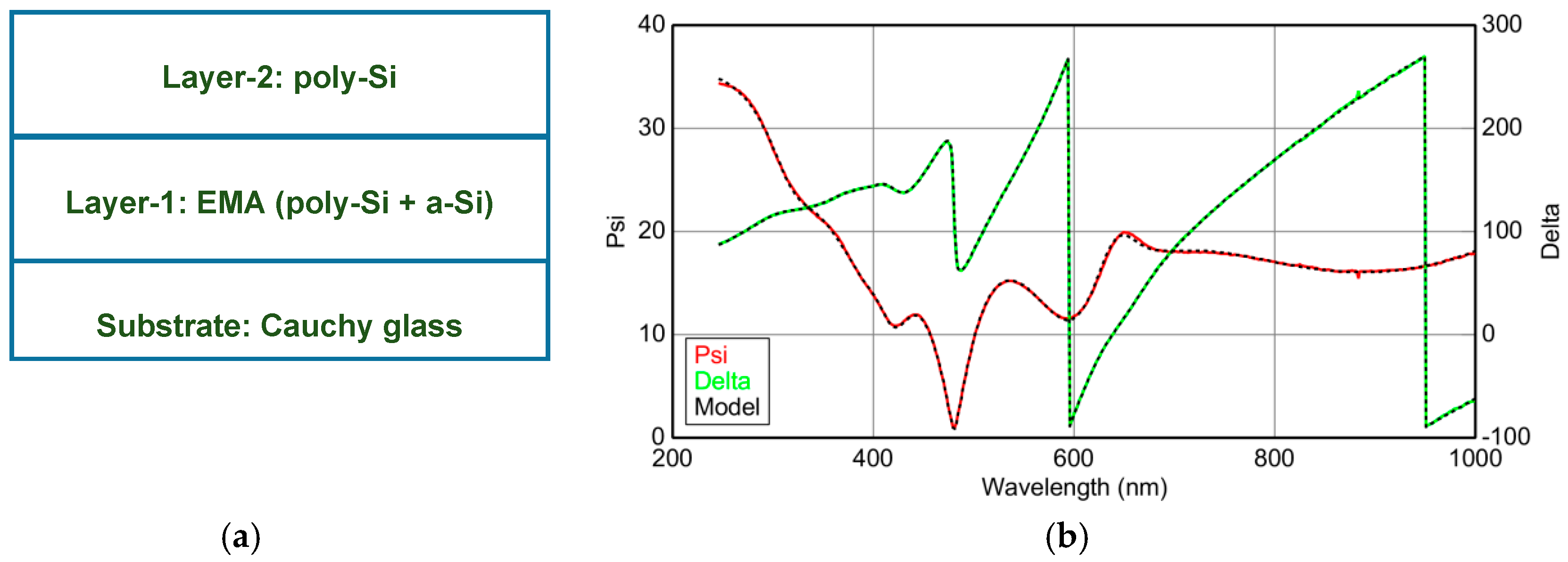
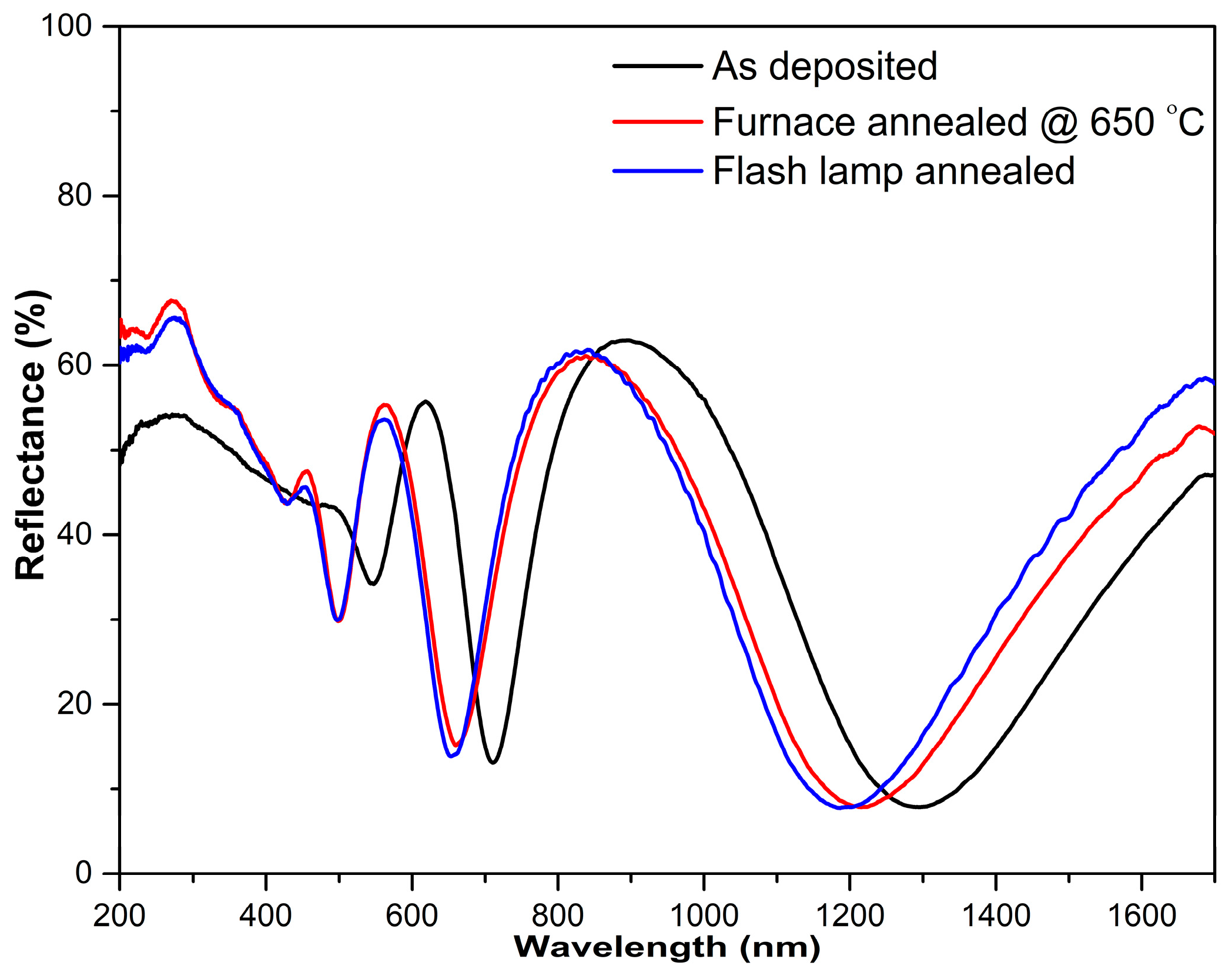
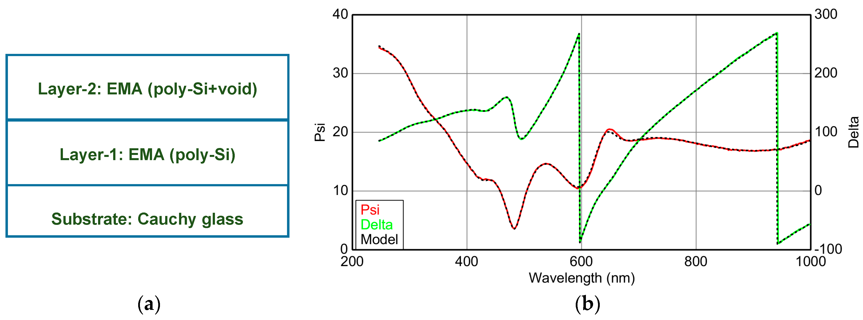
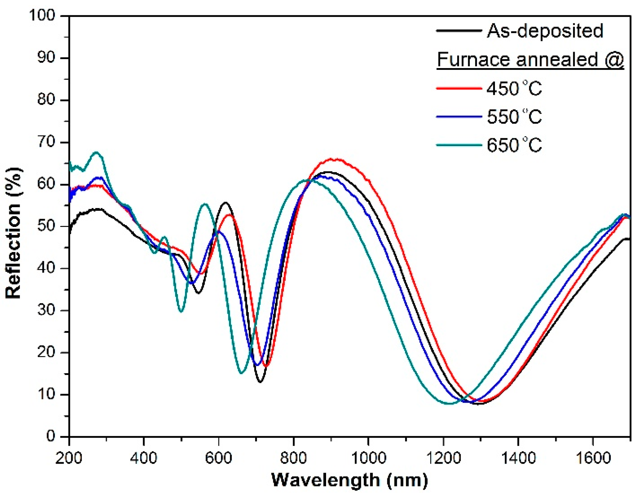
3.1. Optical Properties
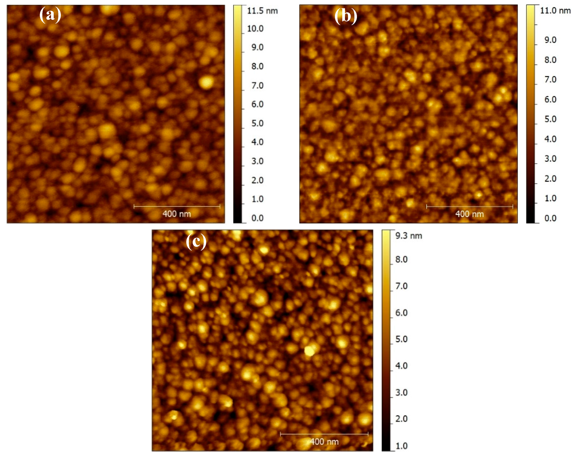
3.2. Surface Topography
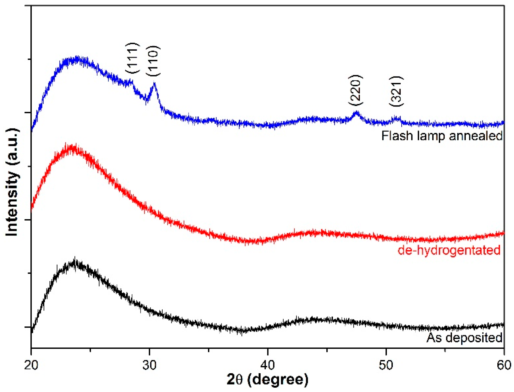
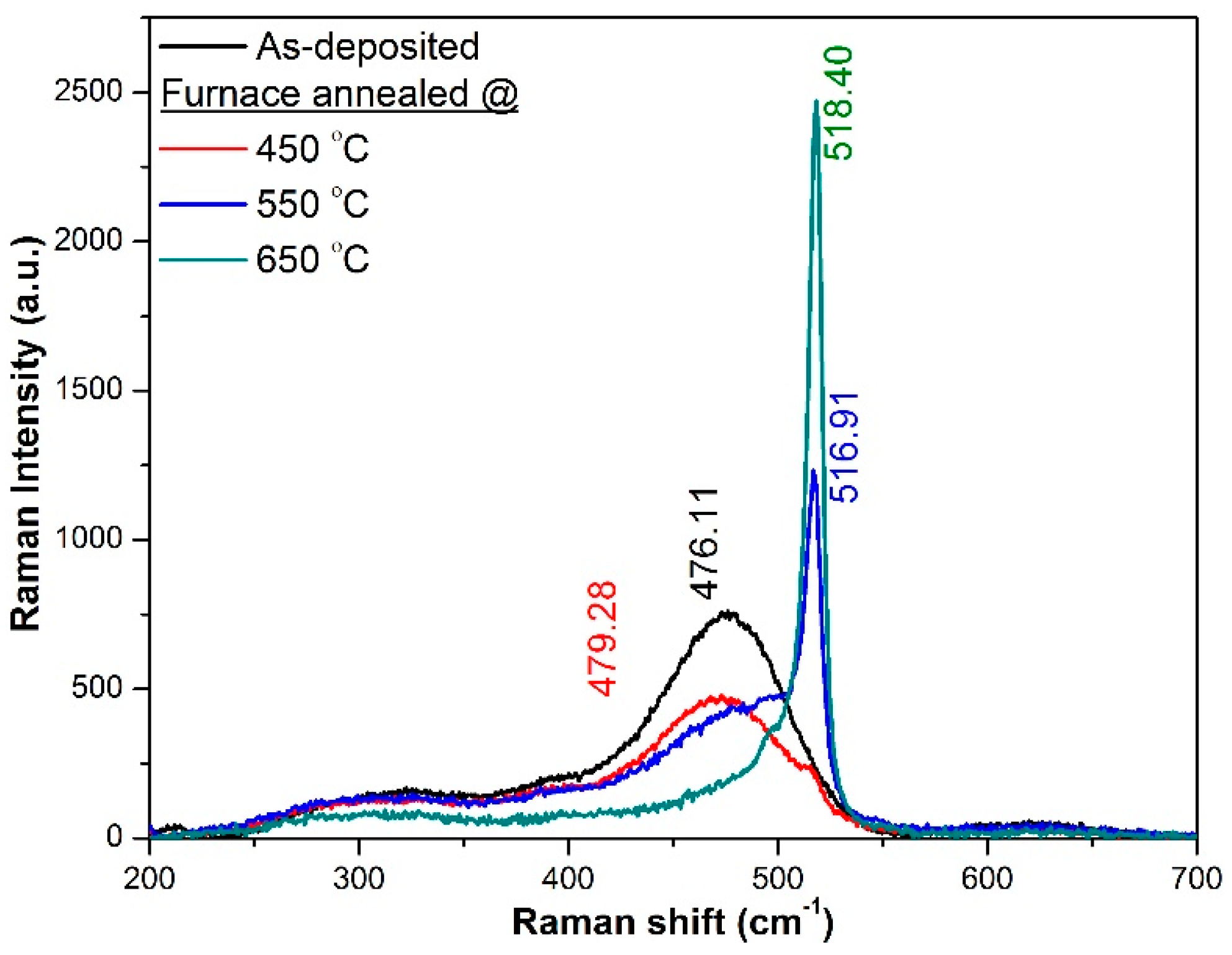
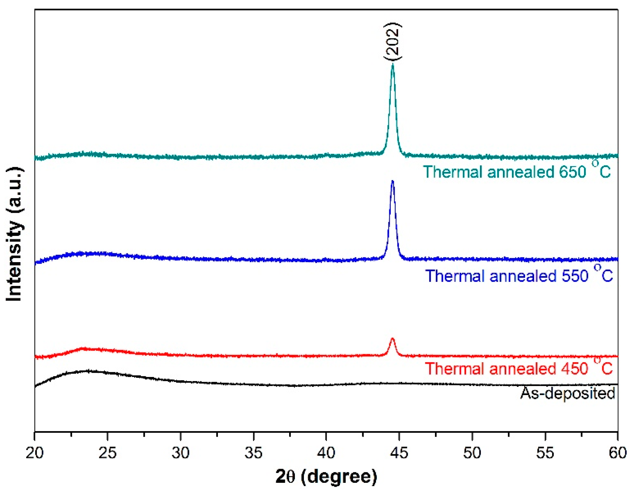
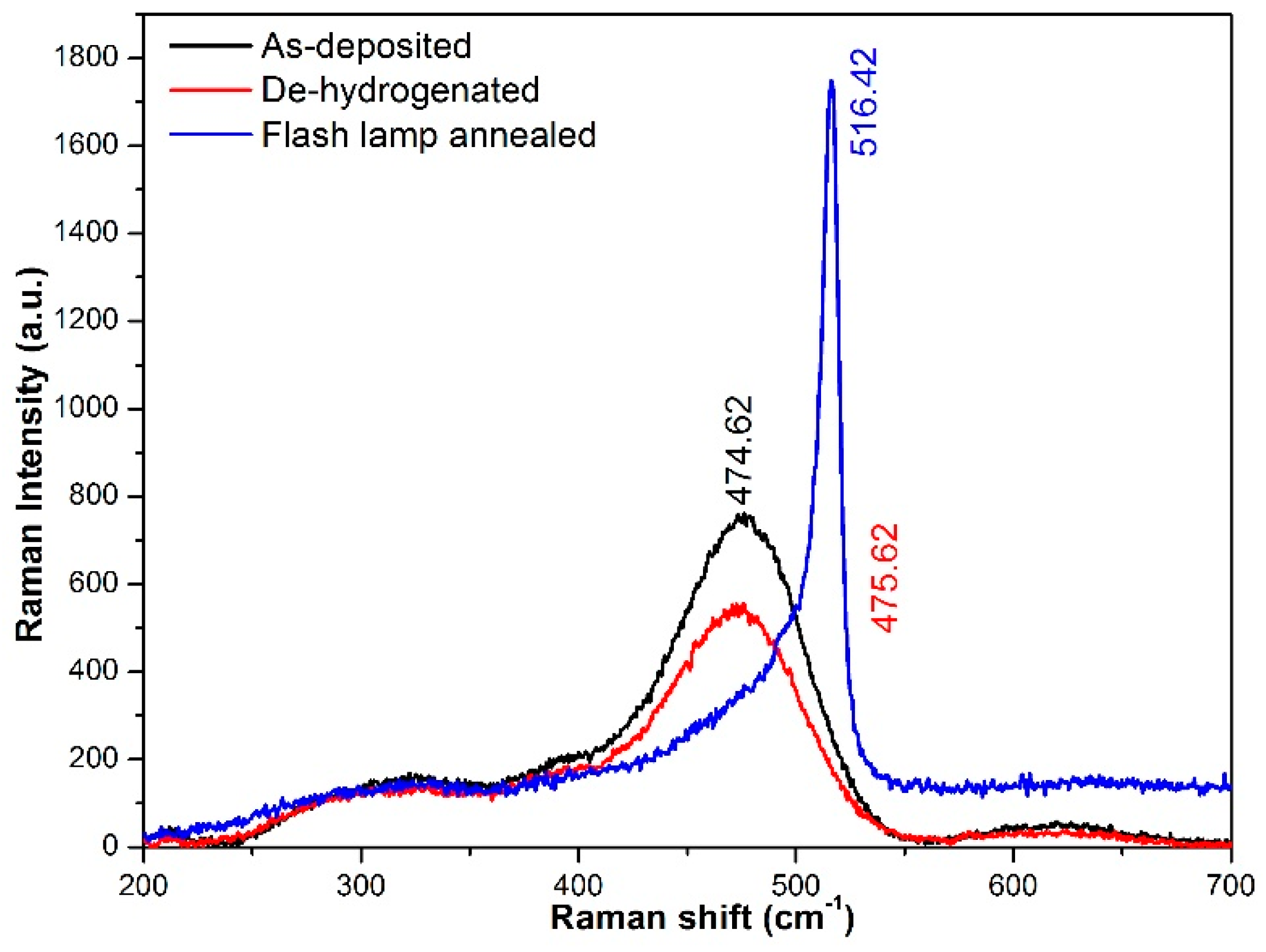
3.3. Crystalline Phase
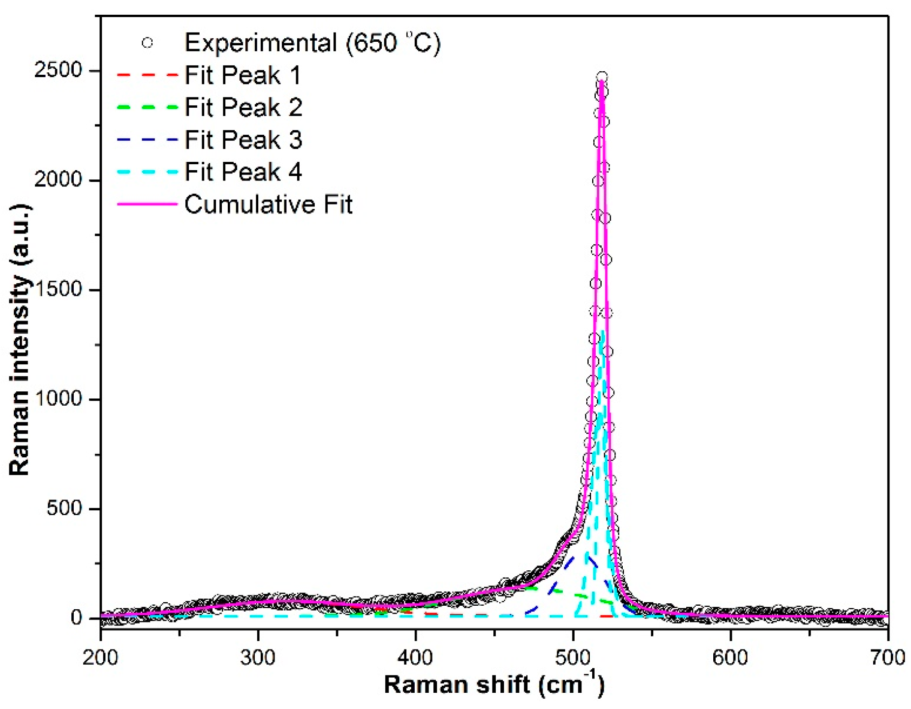
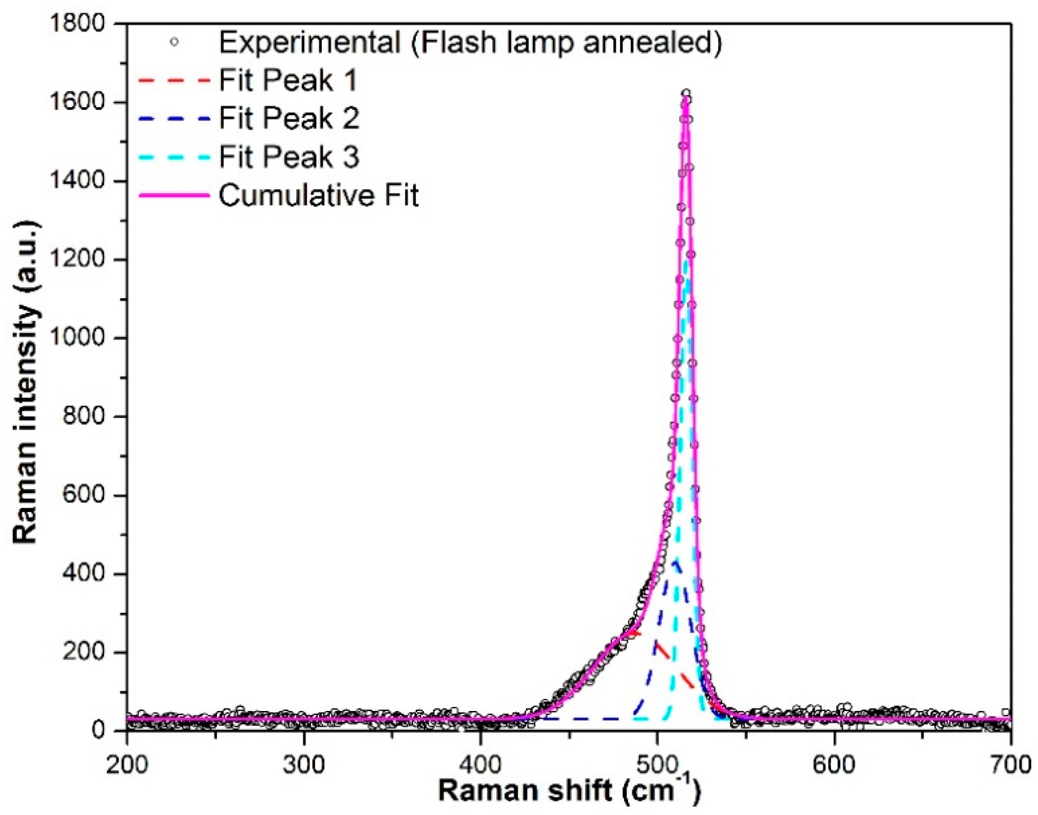
3.4. Crystalline Volume Fraction
4. Conclusions
Acknowledgments
Author Contributions
Conflicts of Interest
References
- Endo, Y.; Fujiwara, T.; Ohdaira, K.; Nishizaki, S.; Nishioka, K.; Matsumura, H. Thin-film polycrystalline silicon solar cells formed by flash lamp annealing of a-Si films. Thin Solid Films 2010, 518, 5003–5006. [Google Scholar] [CrossRef]
- Ohdaira, K.; Endo, Y.; Fujiwara, T.; Nishizaki, S.; Matsumura, H. Formation of highly uniform micrometer-order-thick polycrystalline silicon films by flash lamp annealing of amorphous silicon on glass substrates. Jpn. J. Appl. Phys. 2007, 46, 7603. [Google Scholar] [CrossRef]
- Bergmann, R.B. Crystalline Si thin-film solar cells: A review. Appl. Phys. A 1999, 69, 187–194. [Google Scholar] [CrossRef]
- Tran, N.T.; Keyes, M.P. Polysilicon films prepared by plasma enhanced chemical vapor deposition: Effect of substrate temperatureand annealing temperature. Phys. Status Solidi (a) 1991, 126, K143–K148. [Google Scholar] [CrossRef]
- Yamauchi, N.; Reif, R. Polycrystalline silicon thin films processed with silicon ion implantation and subsequent solid-phase crystallization: Theory, experiments, and thin-film transistor applications. J. Appl. Phys. 1994, 75, 3235–3257. [Google Scholar] [CrossRef]
- Herd, S.R.; Chaudhari, P.; Brodsky, M.H. Metal contact induced crystallization in films of amorphous silicon and germanium. J. Non-Cryst. Solids 1972, 7, 309–327. [Google Scholar] [CrossRef]
- Boyce, J.B.; Mei, P.; Fulks, R.T.; Ho, J. Laser processing of polysilicon thin-film transistors: Grain growth and device fabrication. Phys. Status Solidi (a) 1998, 166, 729–741. [Google Scholar] [CrossRef]
- Pécz, B.; Dobos, L.; Panknin, D.; Skorupa, W.; Lioutas, C.; Vouroutzis, N. Crystallization of amorphous-Si films by flash lamp annealing. Appl. Surf. Sci. 2005, 242, 185–191. [Google Scholar] [CrossRef]
- Yan, B.; Dubey, M.; Shrestha, M.; Fan, Q.; Stevenson, D. Pulsed-lamp crystallization of nanocrystalline silicon thin films for solar cell application. In Proceedings of the 29th European Photovoltaic Solar Energy Conference and Exhibition, Amsterdam, The Netherlands, 22–26 September 2014; pp. 1921–1925. [Google Scholar]
- Ohdaira, K.; Nishizaki, S.; Endo, Y.; Fujiwara, T.; Usami, N.; Nakajima, K.; Matsumura, H. High-quality polycrystalline silicon films with minority carrier lifetimes over 5 µs formed by flash lamp annealing of precursor amorphous silicon films prepared by catalytic chemical vapor deposition. Jpn. J. Appl. Phys. 2007, 46, 7198. [Google Scholar] [CrossRef]
- Ohdaira, K.; Fujiwara, T.; Endo, Y.; Nishizaki, S.; Matsumura, H. Explosive crystallization of amorphous silicon films by flash lamp annealing. J. Appl. Phys. 2009, 106, 044907. [Google Scholar] [CrossRef]
- Ohdaira, K.; Fujiwara, T.; Endo, Y.; Nishizaki, S.; Matsumura, H. Formation of several-micrometer-thick polycrystalline silicon films on soda lime glass by flash lamp annealing. Jpn. J. Appl. Phys. 2008, 47, 8239. [Google Scholar] [CrossRef]
- Ohdaira, K.; Nishikawa, T.; Shiba, K.; Takemoto, H.; Matsumura, H. Drastic suppression of the optical reflection of flash-lamp-crystallized poly-Si films with spontaneously formed periodic microstructures. Thin Solid Films 2010, 518, 6061–6065. [Google Scholar] [CrossRef]
- Terai, F.; Matunaka, S.; Tauchi, A.; Ichimura, C.; Nagatomo, T.; Homma, T. Xenon flash lamp annealing of poly-Si thin films. J. Electrochem. Soc. 2006, 153, H147–H150. [Google Scholar] [CrossRef]
- Jellison, G.E.; Merkulov, V.I.; Puretzky, A.A.; Geohegan, D.B.; Eres, G.; Lowndes, D.H.; Caughman, J.B. Characterization of thin-film amorphous semiconductors using spectroscopic ellipsometry. Thin Solid Films 2000, 377, 68–73. [Google Scholar] [CrossRef]
- Jellison, G.E. Data analysis for spectroscopic ellipsometry. Thin Solid Films 1993, 234, 416–422. [Google Scholar] [CrossRef]
- Aspnes, D.E.; Theeten, J.B.; Hottier, F. Investigation of effective-medium models of microscopic surface roughness by spectroscopic ellipsometry. Phys. Rev. B 1979, 20, 3292. [Google Scholar] [CrossRef]
- Jellison, G.E., Jr. Spectroscopic ellipsometry data analysis: Measured versus calculated quantities. Thin Solid Films 1998, 313, 33–39. [Google Scholar] [CrossRef]
- Santjojo, D.J.; Aizawa, T.; Muraishi, S. Ellipsometric characterization on multi-layered thin film systems during hydrogenation. Mater. Trans. 2007, 48, 1380–1386. [Google Scholar] [CrossRef]
- Bisi, O.; Ossicini, S.; Pavesi, L. Porous silicon: A quantum sponge structure for silicon based optoelectronics. Surf. Sci. Rep. 2000, 38, 1–126. [Google Scholar] [CrossRef]
- Ben Slama, S.; Hajji, M.; Ezzaouia, H. Crystallization of amorphous silicon thin films deposited by pecvd on nickel-metalized porous silicon. Nanoscale Res. Lett. 2012, 7, 464. [Google Scholar] [CrossRef] [PubMed]
- Timoshenko, V.Y.E.; Gonchar, K.A.; Mirgorodskiy, I.V.; Maslova, N.E.E.; Nikulin, V.E.; Mussabek, G.K.; Taurbaev, Y.T.; Svanbayev, E.A.; Taurbaev, T.I. Efficient visible luminescence of nanocrystalline silicon prepared from amorphous silicon films by thermal annealing and stain etching. Nanoscale Res. Lett. 2011, 6, 349. [Google Scholar] [CrossRef] [PubMed]
- Garnett, E.; Yang, P. Light trapping in silicon nanowire solar cells. Nano Lett. 2010, 10, 1082–1087. [Google Scholar] [CrossRef] [PubMed]
- Laaziri, K.; Kycia, S.; Roorda, S.; Chicoine, M.; Robertson, J.L.; Wang, J.; Moss, S.C. High-energy X-ray diffraction study of pure amorphous silicon. Phys. Rev. B 1999, 60, 13520. [Google Scholar] [CrossRef]
- Vallat-Sauvain, E.; Kroll, U.; Meier, J.; Shah, A.; Pohl, J. Evolution of the microstructure in microcrystalline silicon prepared by very high frequency glow-discharge using hydrogen dilution. J. Appl. Phys. 2000, 87, 3137–3142. [Google Scholar] [CrossRef]
- Wei, W.; Xu, G.; Wang, J.; Wang, T. Raman spectra of intrinsic and doped hydrogenated nanocrystalline silicon films. Vacuum 2007, 81, 656–662. [Google Scholar] [CrossRef]
- Leitch, A.W.R.; Alex, V.; Weber, J. Raman spectroscopy of hydrogen molecules in crystalline silicon. Phys. Rev. Lett. 1998, 81, 421. [Google Scholar] [CrossRef]
- Voutsas, A.T.; Hatalis, M.K.; Boyce, J.; Chiang, A. Raman spectroscopy of amorphous and microcrystalline silicon films deposited by low-pressure chemical vapor deposition. J. Appl. Phys. 1995, 78, 6999–7006. [Google Scholar] [CrossRef]
- Tsu, R.; Gonzalez-Hernandez, J.; Chao, S.S.; Lee, S.C.; Tanaka, K. Critical volume fraction of crystallinity for conductivity percolation in phosphorus-doped Si:F:H alloys. Appl. Phys. Lett. 1982, 40, 534–535. [Google Scholar] [CrossRef]


| RF Power (W) | Press. (Torr) | H2 (sccm) | SiH4 (sccm) | Ts (°C) | d (mm) |
|---|---|---|---|---|---|
| 1500 | 5.0 | 10,000 | 100 | 150 | 12 |
© 2018 by the authors. Licensee MDPI, Basel, Switzerland. This article is an open access article distributed under the terms and conditions of the Creative Commons Attribution (CC BY) license (http://creativecommons.org/licenses/by/4.0/).
Share and Cite
Shrestha, M.; Wang, K.; Zheng, B.; Mokrzycki, L.; Fan, Q.H. Comparative Study of Furnace and Flash Lamp Annealed Silicon Thin Films Grown by Plasma Enhanced Chemical Vapor Deposition. Coatings 2018, 8, 97. https://doi.org/10.3390/coatings8030097
Shrestha M, Wang K, Zheng B, Mokrzycki L, Fan QH. Comparative Study of Furnace and Flash Lamp Annealed Silicon Thin Films Grown by Plasma Enhanced Chemical Vapor Deposition. Coatings. 2018; 8(3):97. https://doi.org/10.3390/coatings8030097
Chicago/Turabian StyleShrestha, Maheshwar, Keliang Wang, Bocong Zheng, Laura Mokrzycki, and Qi Hua Fan. 2018. "Comparative Study of Furnace and Flash Lamp Annealed Silicon Thin Films Grown by Plasma Enhanced Chemical Vapor Deposition" Coatings 8, no. 3: 97. https://doi.org/10.3390/coatings8030097
APA StyleShrestha, M., Wang, K., Zheng, B., Mokrzycki, L., & Fan, Q. H. (2018). Comparative Study of Furnace and Flash Lamp Annealed Silicon Thin Films Grown by Plasma Enhanced Chemical Vapor Deposition. Coatings, 8(3), 97. https://doi.org/10.3390/coatings8030097