Abstract
Using the fact that a sub-wavelength structure exhibits the same thermal expansion coefficient as a micro-lens array, we design a micro-lens super-surface film with regular circular hole-like subwavelength structures to realize the high performances of central highly focusing strength and short focal length. In addition, based on the Fresnel—Kirchhoff diffraction theory, the influences of subwavelength structural period and height on the focusing performance of a micro-lens are analyzed. Furthermore, the finite-difference time-domain method is utilized to optimize the structural parameters. Via direct laser writing and an inductively coupled plasma process, we fabricated a square micro-lens array consisting of a 1000 × 1000 micro-lens unit with a sub-wavelength structure, and the optical focusing performance was measured in the visible light band. Finally, the experimental results indicate that the focal length is decreased to 15 μm, the focal spot central energy is increased by 7.3%, and the light transmission, enhanced via inserting sub-wavelength structures, corresponds to 3%. This proves that the designed micro-lens array with a regular-graded circular hole-like subwavelength structure can achieve central high focusing and a short focal length. This has applications in several fields of wavefront detection and light field imaging systems.
1. Introduction
Micro-lens arrays are widely applied in homogenizing systems [1,2], light-field imaging [3,4], and Hartmann sensors [5]. The efficiency of energy utilization is an important parameter of a micro-lens array. An anti-reflection coating is typically deposited on the surface of a micro-lens to decrease reflection and improve the efficiency of energy utilization [6,7]. However, conventional anti-reflection coatings are generally affected by the fact that the material with the desired refractive index is usually either expensive or scare. AR coatings usually have a multilayer-structure, therefore the coefficients of thermal expansion (CTE) can be different between layers, including the substrate. The difference of CTEs may induce stress if the process temperature is different from the environmental temperature. The induced stress can further induce micro-lens deformation or coating delamination.
In existing studies, several subwavelength structures were used to overcome the disadvantages on the surface of the micro-lens [8,9]. Subwavelength structure layer is consistent material with the substrate, and hence the issue of optical deformation due to the difference of CTE is non-existent [10]. Moreover, optimizing the subwavelength structural parameters to achieve different equivalent refractive indexes, thereby resolves the issue of material. Currently, many subwavelength structures on the micro-lens super-surface are fabricated to achieve functions including anti-reflection [11,12,13], filter [14,15], and blazed grating [16]. For example, researchers fabricated a wafer-level micro-lens with a bionic moth-eye nanostructure wherein the transmittance of the micro-lens was increased by approximately 3% under wavelengths in the range of 400–750 nm [17]. A study explored a similar low-loss dielectric micro-lens with a nanopillar array with a variable diameter for infrared (IR) radiation on a silicon substrate [18]. Additionally, an antireflective optical lens with large-area glass nanohole arrays for optical imaging was reported [19,20]. However, most reports have not discussed the study of the focusing performance of micro-lens super-surface [21,22,23], which is extremely important to improve the energy utilization.
In this study, in order to realize the performance of highly focusing and short focal length of the lens, we design a micro-lens super-surface film with a regular graded circular hole-like subwavelength structure. The effects of the period and height of the subwavelength structure on the focusing performance of the micro-lens are analyzed via theory and the finite-difference time-domain (FDTD) method to obtain the optimized structural parameters. The results obtained with respect to the micro-lens super-surface film were prepared via direct laser writing and an inductively coupled plasma process. Finally, we used a Nikon Eclipse 50i microscope to measure the focusing performance of the micro-lens super-surface. This study provides a reference to investigate and produce a micro-miniature micro-lens super-surface element for optical imaging systems.
2. Microstructure Design and Optimization
The focal spot size of the micro-lens array is influenced by the calibre and focal length of the micro-lens. Under the same calibre, a long focal length leads to pronounced diffraction, and this causes the spot to spread. Therefore, the size of the micro-lens array must be designed to consider the effect of diffraction on the spot.
2.1. Design of Micro-Lens Structure Parameters
In this study, the energy efficiency of the micro-lens array is improved via designing a circular hole-like subwavelength structure on the surface of the micro-lens. A micro-lens array that is composed of micro-lens with a 7 μm calibre and 230 nm vector height is selected. The refractive index of the substrate is 1.455, and the ideal focal length based on geometrical optics calculation is 57 μm. The ideal focal length of the micro-lens is affected by Fresnel diffraction, and thus the focus is shifted [24,25].
As shown in Figure 1, we assumed that for the spherical wave after passing through the micro-lens (based on the Fresnel–Kirchhoff diffraction integral formula), the complex amplitude at point on the receiving plane is given as follows:
where is the distance from the surface element to a point on the receiving surface, is the angle between and , and is the radius of the outgoing spherical wave.
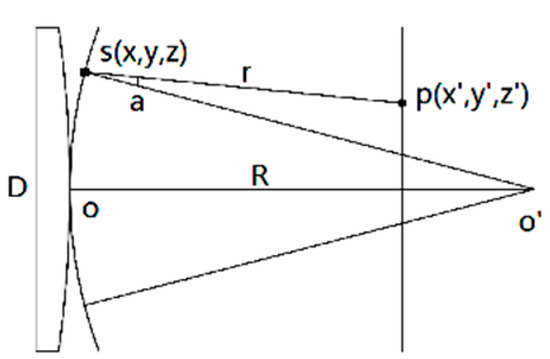
Figure 1.
Amplitude distribution of spherical wave passing through the micro-lens at point P on the receiving plane.
The Fresnel coefficient of the spherical wave corresponds to , where denotes the diameter of the micro-lens unit. The on-axis focused light intensity distribution is given by the Collins formula as follows [26,27]:
where , and denotes the relative focal shift.
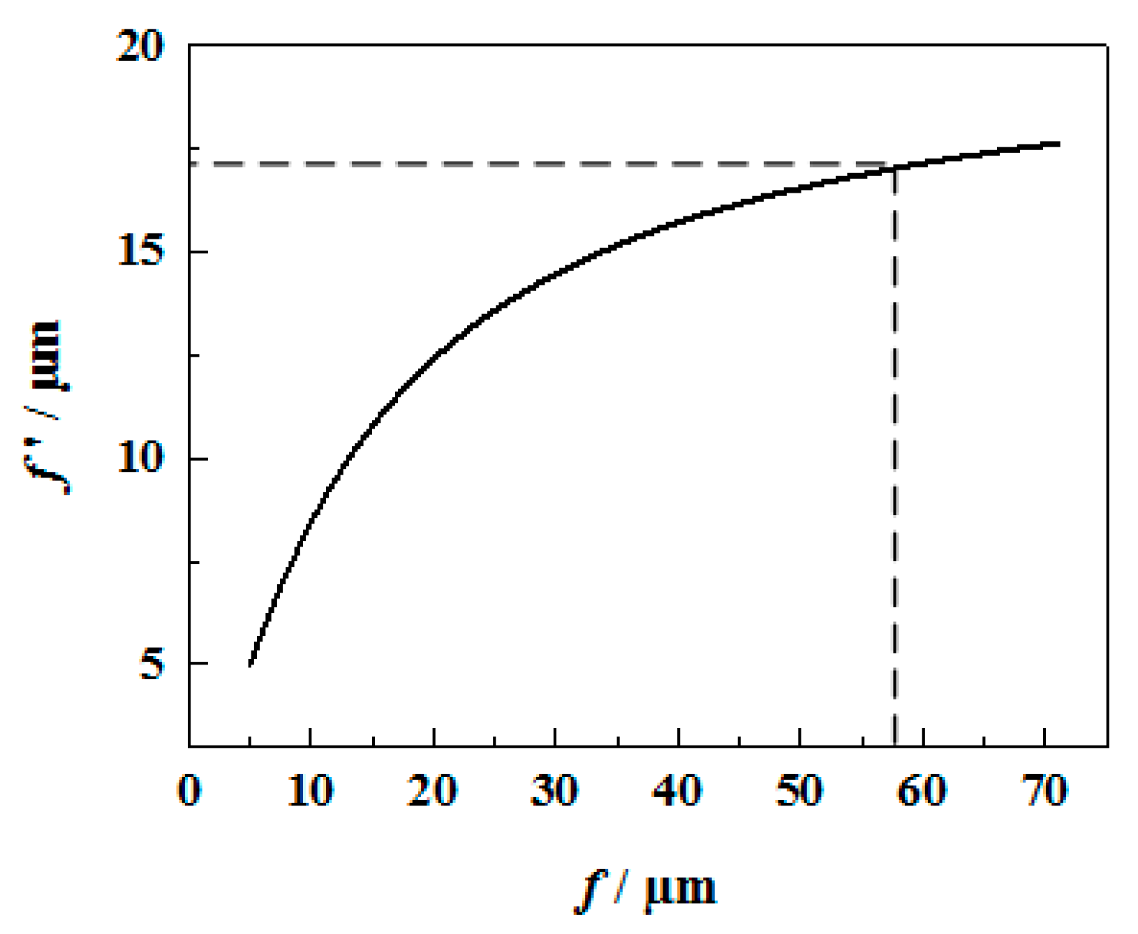
The relationship between theoretical focal length and actual focal length is calculated via MATLAB R2018a as shown in Figure 2. The abscissa denotes the theoretical focal length of the geometrical optics calculation. Therefore, the actual focal length of the micro-lens designed is 17 μm.
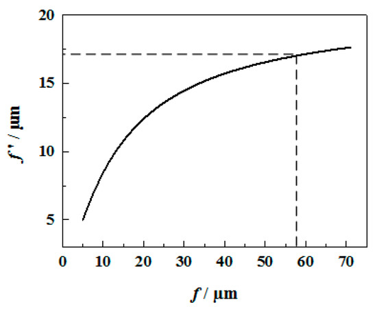
Figure 2.
The relationship between the actual focal length of the micro-lens and theoretical focal length obtained by relative focal shift (the diameter of the micro-lens D = 7 μm).
2.2. Design of the Subwavelength Structure of the Micro-Lens
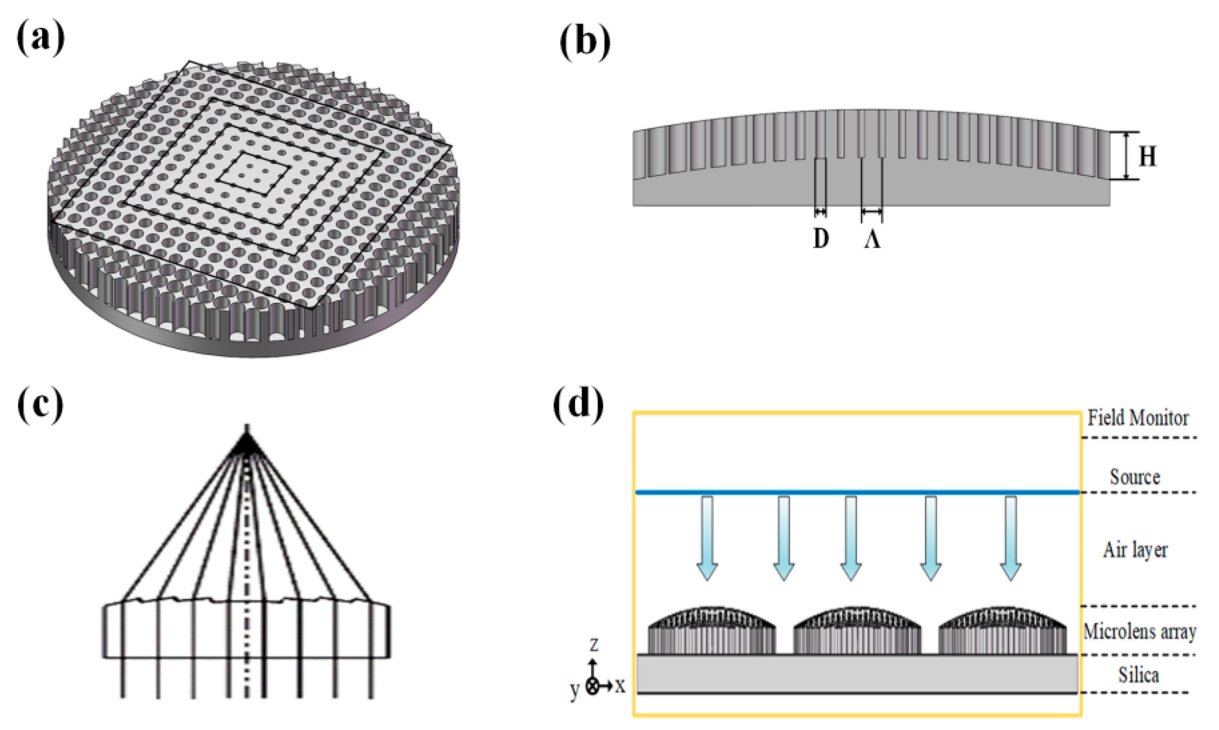
The subwavelength structure on the curved surface should consider whether high-order diffraction occurs with respect to oblique incident light waves. Based on the rigorous coupled wave theory, to ensure that the oblique incident light wave passes through the subwavelength structure without high-order diffraction, the period should satisfy the condition: , where denotes the structural period, the wavelength of the incident light wave, the refractive index of air, and the refractive index of the micro-lens. Since the micro-lens array is prepared on the surface of the fused silica, the micro-lens and fused silica have the same refractive index. We assume that the incident light nm, air refractive index and micro-lens refractive index . The period value range corresponds to (0 nm, 204 nm) and the selected period value is 200 nm. As shown in Figure 3a, five circular-hole subwavelength ring-band structures are distributed on the surface of the micro-lens unit cell, wherein the diameter of the center hole is small and diameter of the edge hole is large. The geometric parameters of a band unit are given in Figure 3b. The parameters consist of the period , structural height , and structural diameter . The diameter of the circular hole is equally increased from the center to the edge as follows: 30, 60, 90, 120, and 150 nm. As indicated by the rigorous coupled wave theory, increases in the radius of the circular hole-like subwavelength structure decrease the refractive index of the subwavelength structural layer wherein the convergence schematic is shown in Figure 3c. Based on film theory, the structural height is calculated as follows: .
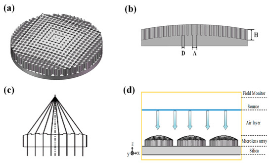
Figure 3.
Equivalent schematic of the micro-lens focus of the circular hole-like subwavelength structure: (a) distribution of the circular hole-like subwavelength structure (3D) diagram of the simulated model; (b) the distribution of the circular hole-like subwavelength structure (2D) cross-section of the model; (c) focusing diagram of converging micro-lens; (d) schematic diagram of the finite-difference time-domain (FDTD) simulation model.
Based on the rigorous coupled wave theory, the circular hole-like subwavelength structural parameters of the gradual distribution are as follows: the period is 200 nm, the height is 104 nm, and the diameter of the circular hole corresponds to the difference change from the center to the edge as follows: 30, 60, 90, 120, and 150 nm.
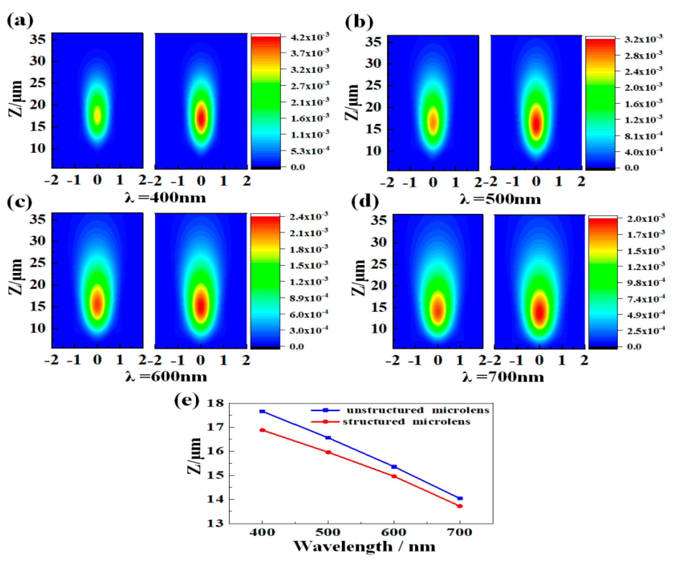
The commercial software Lumerical FDTD Solutions 2018a is applied to calculate the Poynting vector distribution of the proposed substructure. The FDTD simulation model is built in x-y-z axis space rectangular coordinate system shown in Figure 3d, which includes a silica substrate, the micro-lens array, air layer, source, and field monitor. The FDTD Solutions uses the plane wave source with a polarization direction along the x axis, and the boundary conditions correspond to perfect matched layer (PML) boundary conditions. Figure 4a–d show the focusing light intensity distribution in the x-z plane on the surface of the unstructured (left) and structured micro-lens (right) for the incident light wavelength of 400, 500, 600, and 700 nm, respectively. Additionally, the focal length changes with the incident wavelength are shown in Figure 4e. The blue line indicates the focal length of the unstructured micro-lens, and the red line indicates the focal length of the structured micro-lens. As shown in Figure 4, in the 400–700 nm wavelength range, the micro-lens with the subwavelength structure exhibits a good highly focusing effect, and the focal length value is lower than that of the unstructured micro-lens. This proves that the regularized circular hole-like subwavelength structure decreases the focal length of the micro-lens and increases the depth of the field. The focal length decreases when the incident wavelength increases. Additionally, the central energy of the structured micro-lens (right) also exceeds that of the unstructured micro-lens (left). Therefore, it is possible to change the focal length and center energy of the micro-lens by adjusting the period and height of the subwavelength structure.

Figure 4.
(a–d) Simulated intensity profiles in the x-z plane for the micro-lens at wavelengths λ = 400, 500, 600, and 700 nm, respectively: unstructured micro-lens (left) and structured micro-lens (right); (e) simulated focal length as a function of the incident wavelength.
2.3. Parameters of the Optimized Subwavelength Structure of Micro-Lens
After the plane wave is incident on the super-surface of the equivalent refractive index radial gradation, the phase difference is generated in the place where the equivalent refractive index is different represented as follows: . A phase change of is achieved as the height changes in the subwavelength structure.
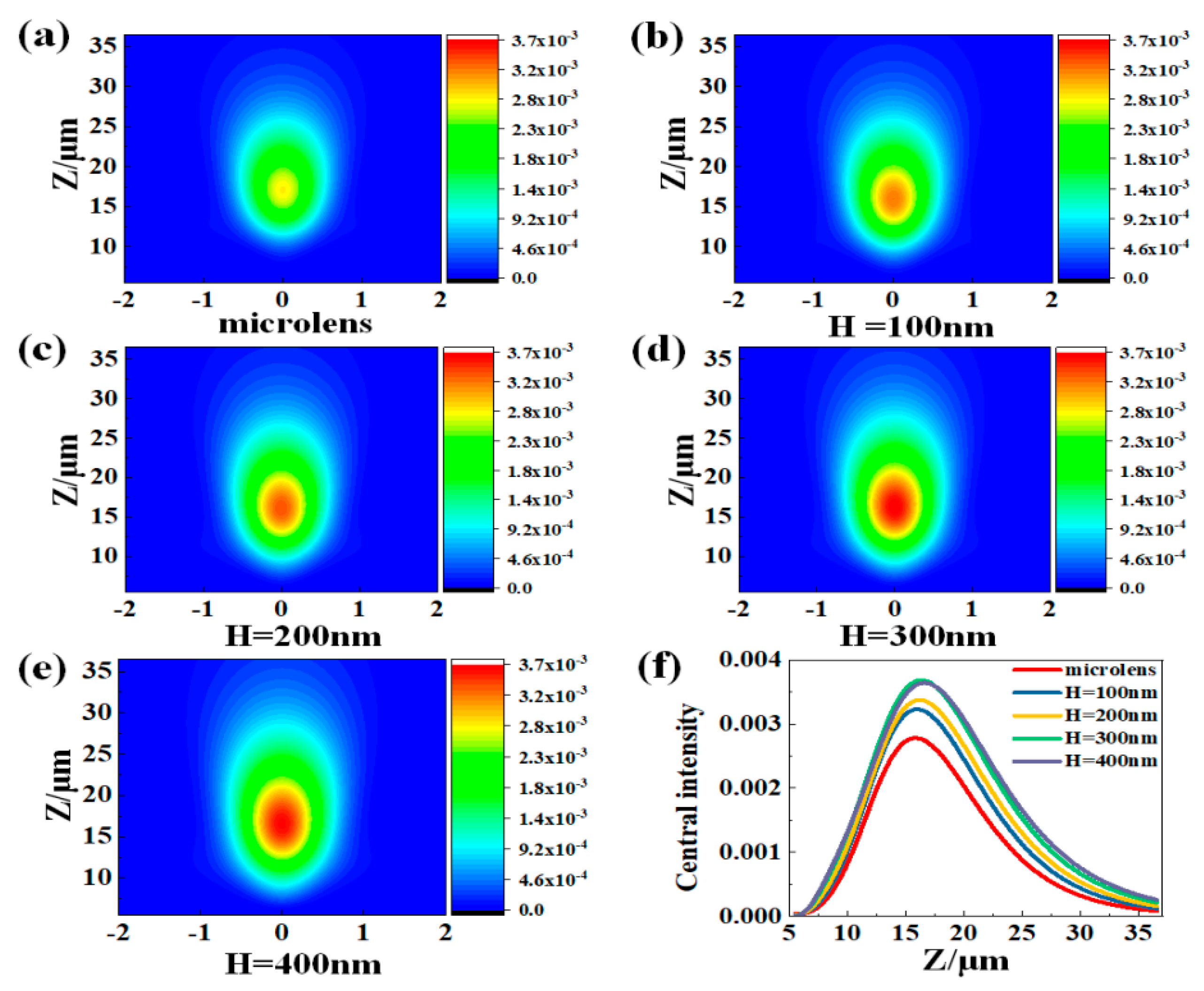
The FDTD method is used to optimize the micro-lens subwavelength structure with a graded circular hole array at the wavelength nm to obtain a better focusing performance and evaluate the effects of height and period . Figure 5 shows the x-z plane field intensity distribution and center energy curve of the micro-lens along the z-axis. Figure 5a shows the electric field distribution of the unstructured micro-lens. Figure 5b–e show the electric field distributions of the structured micro-lens with heights of 100, 200, 300, and 400 nm, respectively. The diameter of each ring hole of the structured micro-lens corresponds to 30, 60, 90, 120, and 150 nm, and the structural period is 200 nm. As shown in the figure, the central intensity of the structured micro-lens exceeds that of the unstructured micro-lens. Additionally, when the height of the structure is from 100 to 300 nm, central intensity of the focal spot increases as height increases. When the height is from 300 to 400 nm, the central intensity value does not vary significantly when height increases. Figure 5f shows the central intensity distribution of each structure at the focus. As shown in the figure, the focal length of the structured micro-lens is lower than that of the unstructured micro-lens, and the focal length increases when structural height increases. Based on the results, the height of the structure is selected as 300 nm.

Figure 5.
Simulated intensity profiles in the x-z plane (y = 0) of unstructured and structured micro-lens with different heights at the wavelength nm: (a) unstructured micro-lens; (b) nm; (c) nm; (d) nm; (e) nm; (f) the central intensity curve of each focal spot along the z-axis.
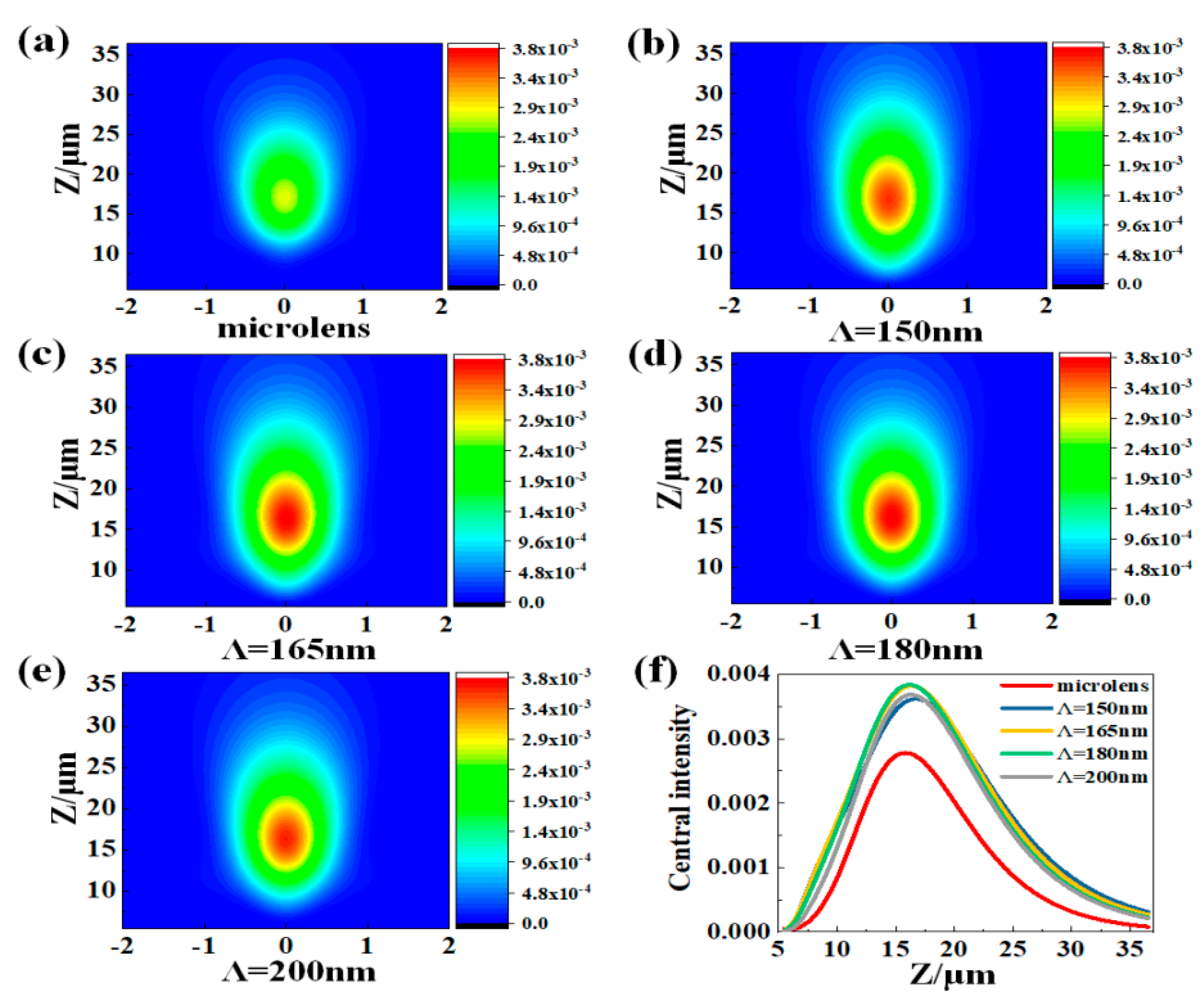
In addition to the height factor, the effect of the structural period is also analyzed. The x-z plane field intensity distribution and center energy curve of the micro-lens along the z-axis are shown in Figure 6. Figure 6a shows the electric field distribution of the unstructured micro-lens. Figure 6b–e show the electric field distributions of the structured micro-lens with periods of 150, 165, 180, and 200 nm, respectively. The diameter of each ring hole of the structured micro-lens corresponds to 30, 60, 90, 120, and 150 nm, and the structural height is 300 nm. As shown in the figure, the central intensity of the structured micro-lens exceeds that of the unstructured micro-lens. When the period increases, it tends to initially increase and then decrease. Specifically, the micro-lens with nm exhibits the highest central intensity. Figure 6f shows the central intensity distribution at the focus along the z-axis. As shown in the figure, the focal length of the structured micro-lens is lower than that of the unstructured micro-lens, and the focal length initially decreases and then increases with increases in the structural period. The focal length of the micro-lens with nm is the lowest. Therefore, when the period is 180 nm, the micro-lens exhibits the best focusing effect.

Figure 6.
Simulated intensity profiles in the x-z plane (y = 0) of the unstructured and structured micro-lens with different periods at the wavelength nm: (a) unstructured micro-lens; (b) nm; (c) nm; (d) nm; (e) nm; (f) central intensity curve of each focal spot along the z-axis.
3. Experiment and Measurements
In this study, we prepare the micro-lens super-surface with a regular graded circular hole-like subwavelength structure via direct laser writing and the inductively coupled plasma (ICP) process. The micro-lens array that is composed of micro-lenses with 7 μm calibre and 230 nm vector height. The circular hole-like subwavelength structure parameters are as follows: period is 180 nm, height is 300 nm, and the diameter of the circular hole is equal to difference change from the center to the edge as follows: 30, 60, 90, 120, and 150 nm.
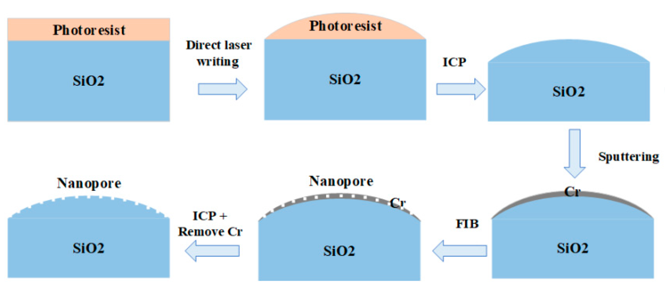
The fabrication process of the micro-lens with subwavelength structure is shown in Figure 7. The details of the fabrication are given below:

Figure 7.
The fabrication process of the regular graded circular hole-like subwavelength structure on the micro-lens surface.
Spin coating: The quartz wafer is cleaned via ultrasonic cleaning, oscillation, and spin coating the photoresist (PR), soft baked (100 °C, for 1 min) via a hot plate (EH45B) to improve the adhesion and uniformity of the photoresist.
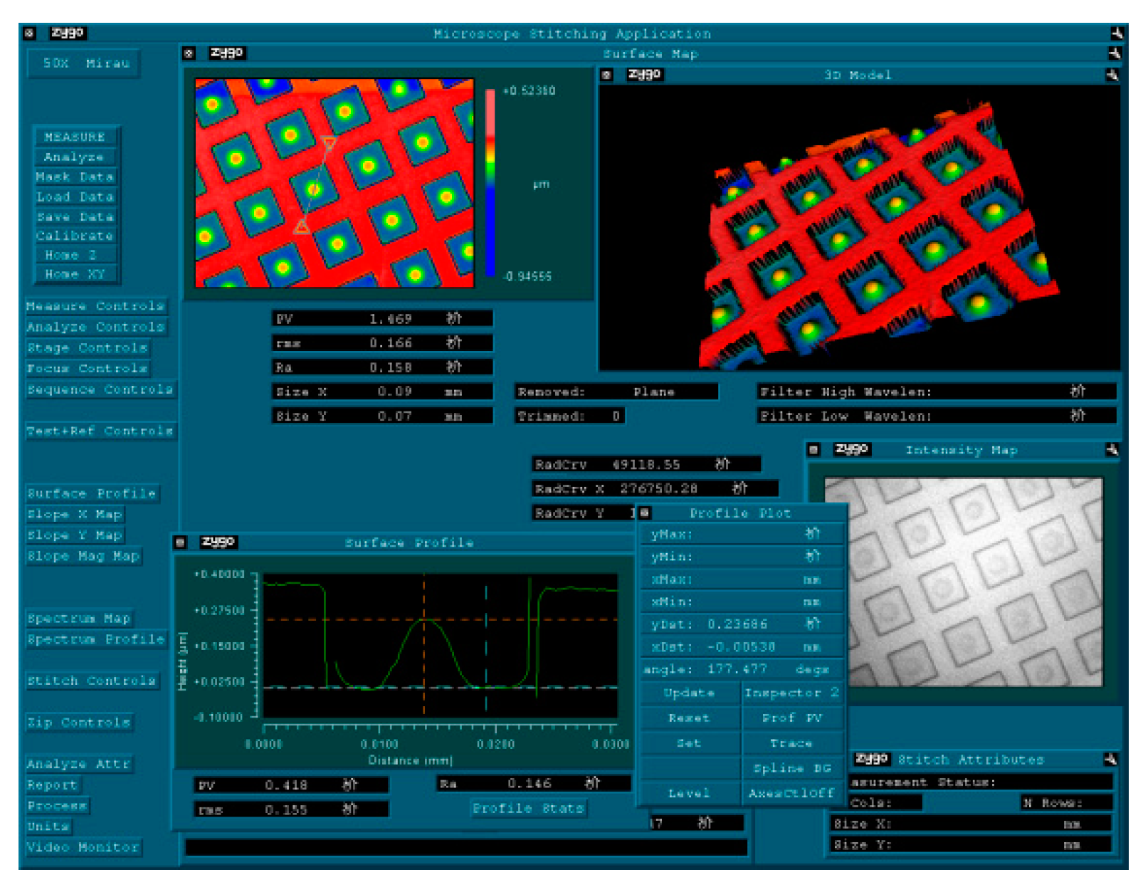
Direct laser writing micro-lens mask: Calibre and vector height parameters of the designed micro-lens are converted into phase distribution maps. The 2D grayscale images of the surface height are edited via MATLAB R2018a, imported into the computer, the mask pattern is then fabricated via the direct laser writing machine (Heidelberg Instruments, DWL66FS, Heidelberg, Germany), and so a micro-lens array with 7 μm diameter and 230 nm vector height is written. The direct write parameters are as follows, power: 70 mW, AOD: 1650, exposure rate: 16.2 mm/s, and exposure time of each pulse: 60 s. Development is performed via the developer AZ300MIF to obtain the mask pattern of the micro-lens. Figure 8 shows the resulting image measured via the interferometer (ZYGO, New View 7100, Middlefield, CT, USA).

Figure 8.
Topography measurement diagram of the micro-lens with 7 μm calibre and 230 nm vector height via the New View 7100 ZYGO interferometer.
ICP etching: The pattern on the photoresist is plasma etched onto the quartz substrate via ICP etching. The etching rate corresponds to 1:1 via adjusting the etching gas ratio and etching time. Etching parameters are as follows: ICP: 230 W, RF: 90 W, pressure: 0.2 Pa, flow: 5 sccm, flow: 20 sccm, and etching time: 30 s.
Sputtering Cr: A 50 nm thick chromium (Cr) layer is plated on the quartz surface via a sputter coater (Alliance Concept, DP650, Annecy, France). The sputtering process parameters are as follows: Ar gas flow: 20 sccm, sputtering time: 70 s, current: 0.6 A, and voltage: 250 V.
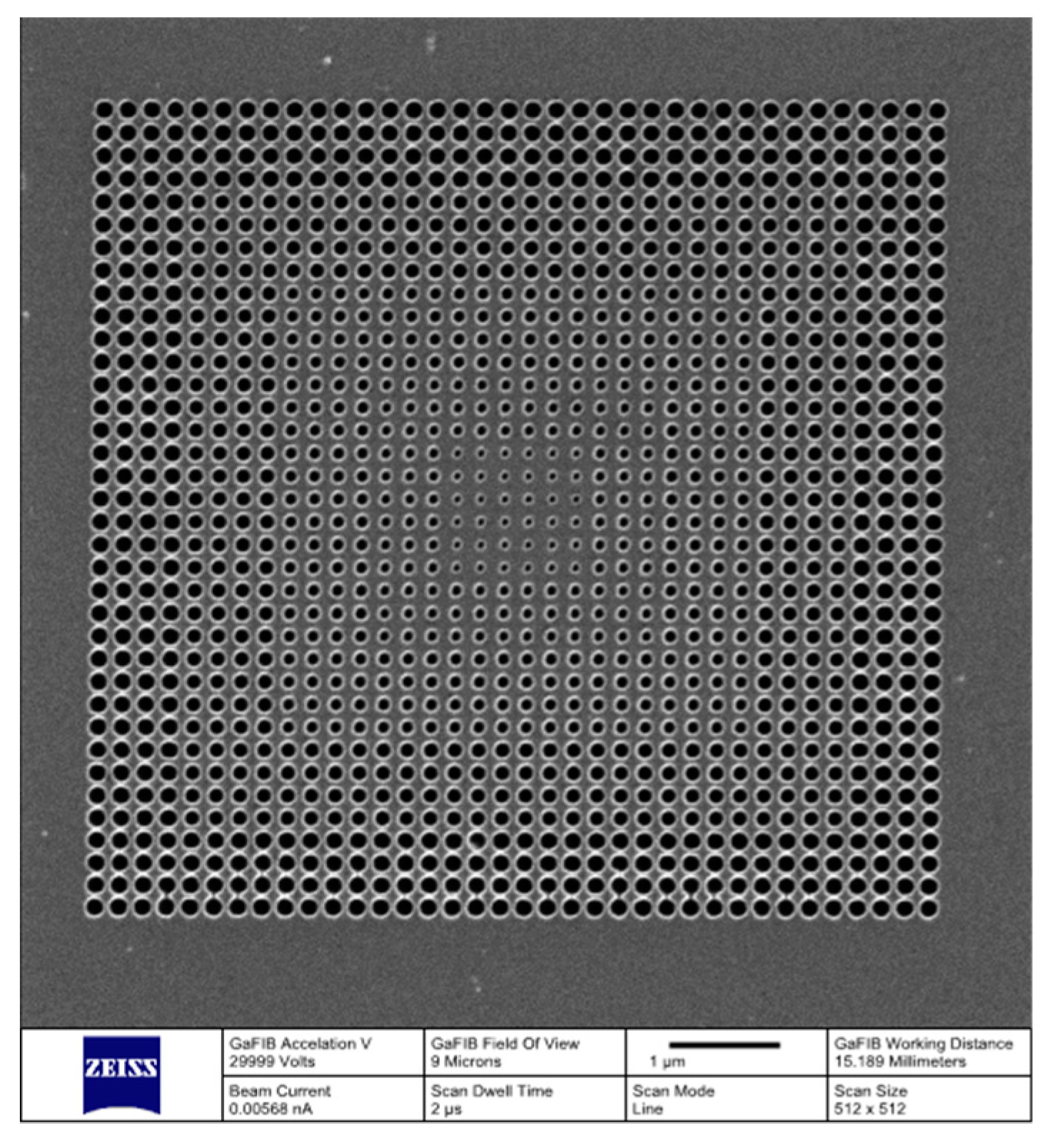
Focused Ion beam (FIB) etching Cr mask: A regular gradient circular hole pattern is written on the micro-lens array with a Cr mask on the surface via focused ion beam (ZEISS, ORION NanoFab, Oberkochen, Germany) direct writing. Etching parameters are as follows: the voltage: 10 kV, ion emission current is a Ga beam, and beam current: 10 pA. Figure 9 shows a scanning electron microscope image of the results.

Figure 9.
The SEM result of the regular graded circular hole-like subwavelength structure mask written by FIB. The scale is 1 μm.
ICP etching: The shape of the circular hole on the mask is etched on the micro-lens via ICP etching. Finally, the remaining Cr is removed with etching solutions and the expected subwavelength structure is then obtained.
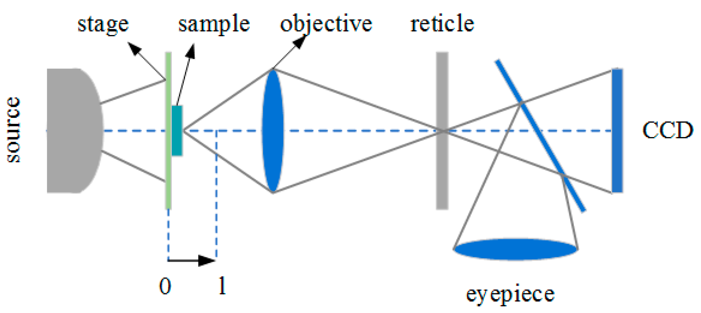
To measure the energy and focal length of the converging spot of a micro-lens with the subwavelength structure, we use a microscope (Nikon, Eclipse 50i, Tokyo, Japan) to measure the focal length of the spot using visible light transmission mode. The charge coupled device (CCD) is used to record the spot image of the sample from position 0 to l. The spot size and energy distribution are calculated from the gray value of the obtained CCD image. The measurement principle is shown in Figure 10.

Figure 10.
Measurement principle of the focused spot passing unstructured micro-lens array and structured micro-lens array from position 0 to l.
There are coarse gears and micro gears on both sides of the microscope to adjust the stage. We place the sample on the stage and turn the coarse gear to determine the micro-lens array. Additionally, we rotate the micro-gear with scale to test the focal length of the micro-lens array. The micro-gear rotates one grid, and the stage moves by 1 μm. We adjust the distance between the stage and objective lens to detect the focal spot pattern at different positions. The patterns are recorded, and the data is analyzed.
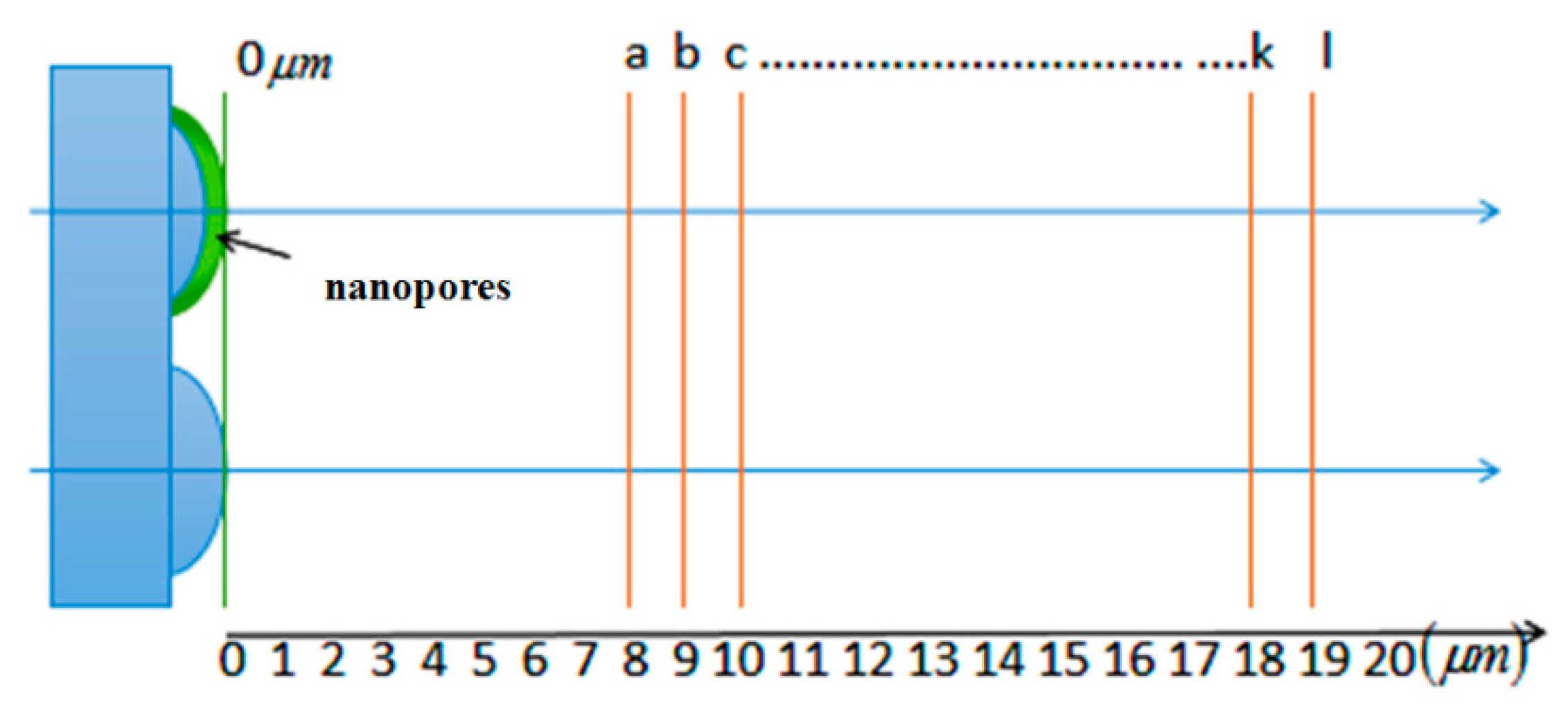
As shown in Figure 11, the a–l position indicates that the microscope observation surface is located at a distance ranging from 8 to 19 μm from the micro-lens array and each position is separated by 1 μm.

Figure 11.
Schematic diagram of the focal length test from micro-lens array surface to observation surface. Each position is separated by 1 μm from a to l position.
4. Results and Discussion
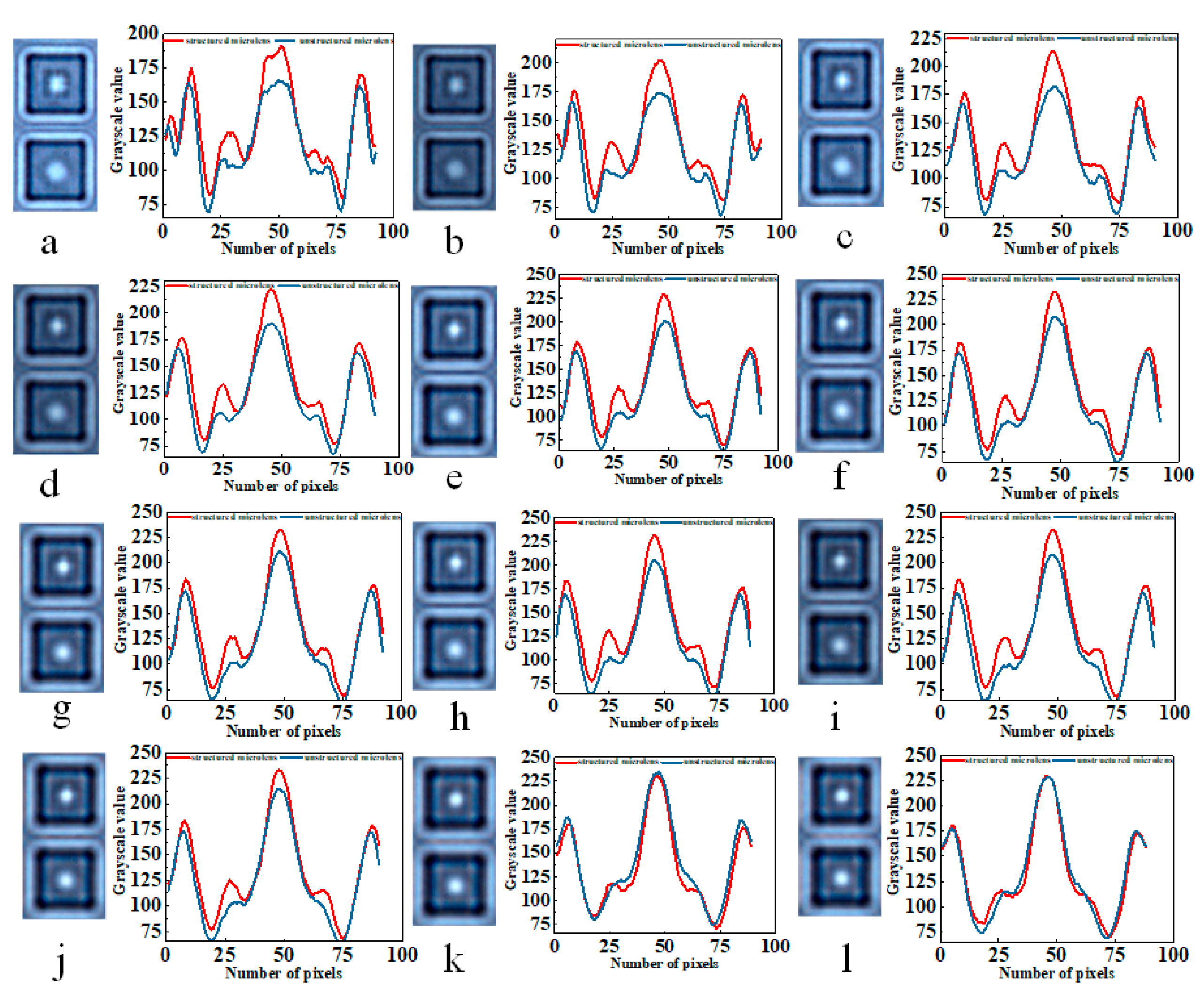
Figure 12 shows the focal spots and gray power distributions obtained per 1 μm from a to l at a magnification of 100×. The two rectangle areas correspond to where the micro-lens is laid. The upper and nether areas represent the focal spots with and without subwavelength structure, respectively. We consider the sample of focal spots on the left side and express the power using gray level to obtain the energy distributions curve at the right side. It is observed from the energy distributions curve that the energy of the focal spots exhibit an evident improvement when fabricated with sub-wavelength structures.

Figure 12.
Convergence spot pattern and energy curve at (a–l) different locations. The upper and nether areas represent the focal spots with and without subwavelength structure, respectively. The blue line represents the grayscale value of unstructured micro-lens, the red line represents the grayscale value of structured micro-lens.
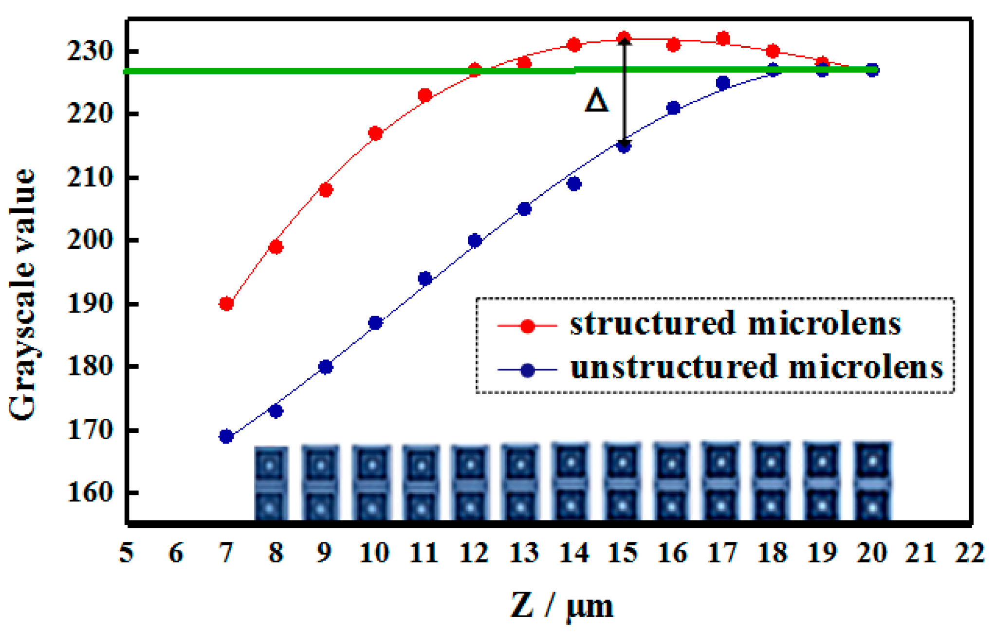
Figure 13 shows the change in energy value at the center of the concentrated spot at different locations. The micro-lens with the subwavelength structure indicates that the center energy of the spot exceeds that of the micro-lens without a subwavelength structure in the range of 8–19 μm. After 19 μm, the energy distributions of the two types of micro-lens are almost identical, and the center energy at the focus (15 μm position) increases by Δ = 7.3% when compared to the unstructured micro-lens. Additionally, the focal length decreases to 15 μm, thereby proving that the micro-lens with the subwavelength structure adequately improves the focusing effect.

Figure 13.
Changes in the energy value of the concentrated energy curve at different locations. The blue line represents the central grayscale value of unstructured micro-lens, the red line represents the central grayscale value of the structured micro-lens.
Furthermore, after the light beam passes through the micro-lens, the energy is concentrated on the optical axis and the anti-reflection and enhanced-transmission are also realized. Based on the rigorous coupled wave and equivalent medium theory, the subwavelength structures are arranged in an annular band distribution on the micro-lens surface. The refractive index of the equivalent medium between different zones is different, the diameter of the center hole is low, and the diameter of the edge hole is high. Thus, the equivalent refractive index from the inner ring to the outer ring gradually decreases. Light passing through the graded index structure can decrease the reflection.
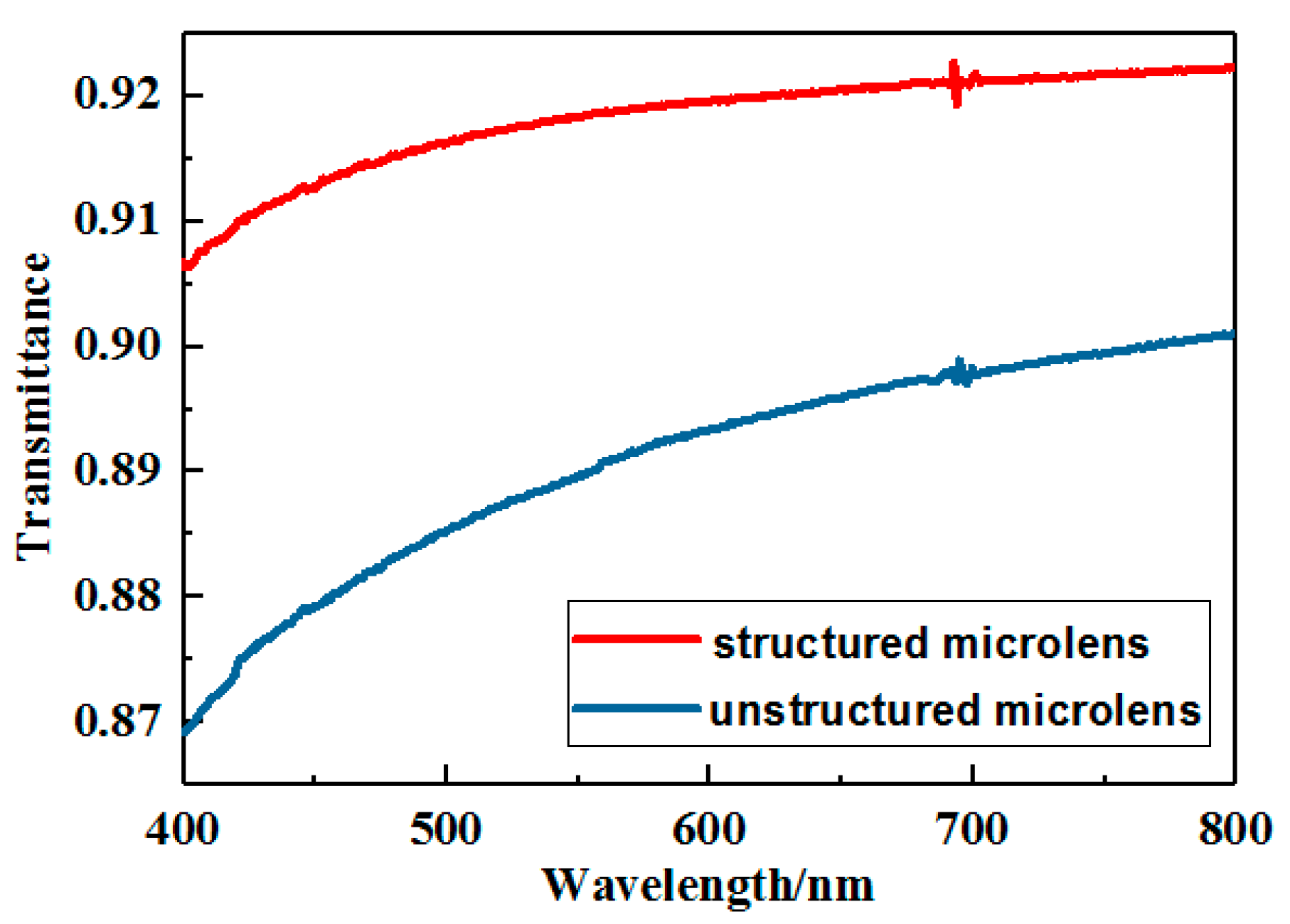
Figure 14 shows the measured transmittance of the unstructured and structured micro-lens in the visible range by using a UV-visible spectrophotometer (Perkin Elmer, Lambda 35, Waltham, MA, USA). The measurement results indicate that the structured micro-lens exhibits higher transmittance than the unstructured micro-lens. The average transmittance of structured micro-lens reaches approximately 91.8% in the 400–800 nm range, thereby indicating that the sub-wavelength structure exhibits good anti-reflection ability. Therefore, it exhibits significant improvement in terms of the energy utilization of the micro-lens.

Figure 14.
Transmittance of the unstructured and structured micro-lens in the visible region. The blue line represents the transmittance curve of unstructured micro-lens, the red line represents the transmittance curve of structured micro-lens.
5. Conclusions
In this study, a micro-lens super-surface with a regularly graded circular hole-like subwavelength structure was designed and fabricated to realize the high performances of central highly focusing and short focal length. We proved that the micro-lens super-surface with a regularly graded circular hole-like subwavelength structure has better focusing properties than a normal micro-lens array. The effect on the focusing performance and focal length modulation of micro-lens super-surface was discussed using the FDTD method. The optimized subwavelength structure is fabricated via direct laser writing and the ICP process. The experimental results and the simulated results have good consistency in the visible light range. The micro-lens super-surface with a regularly graded circular hole-like subwavelength structure realizes a great performance in highly focusing and short focal length. In addition, the super-surface with the subwavelength structure also increases the transmittance, thereby improving energy utilization, which is extremely significant for imaging and detection systems.
Author Contributions
Conceptualization, J.W. and Y.F.; Methodology, J.W.; Software, J.W. and L.Z.; Validation, J.W. and L.Z.; Formal analysis, J.W.; Investigation, Y.L., Y.Z. and B.Y.; Resources, Y.L. and Y.Z.; Data Curation, Y.Z. and B.Y.; Writing-Original Draft Preparation, J.W. and L.Z.; Writing-Review and Editing, Y.F.; Supervision, Y.F.; Project Administration, Y.F.; Funding Acquisition, Y.F.
Funding
This research was funded by National Natural Science Foundation of China (Nos. 51505078, 61705018) and the 111 Project of China (No. D17017).
Acknowledgments
The authors thank the Key Laboratory of Advanced Optical System Design and Manufacturing Technology of the universities of Jilin Province for the SEM technical support.
Conflicts of Interest
The authors declare no conflict of interest.
References
- Zhang, D.; Xu, Q.; Fang, C.; Wang, K.; Wang, X.; Zhuang, S.; Dai, B. Fabrication of a microlens array with controlled curvature by thermally curving photosensitive gel film beneath microholes. ACS Appl. Mater. Interfaces 2017, 9, 16604–16609. [Google Scholar] [CrossRef] [PubMed]
- Jin, Y.; Hassan, A.; Jiang, Y. Freeform microlens array homogenizer for excimer laser beam shaping. Opt. Express 2016, 24, 24846–24858. [Google Scholar] [CrossRef] [PubMed]
- Li, S.-N.; Yuan, Y.; Liu, B.; Wang, F.-Q.; Tan, H.-P. Influence of microlens array manufacturing errors on light-field imaging. Opt. Commun. 2018, 410, 40–52. [Google Scholar] [CrossRef]
- Li, T.J.; Li, S.; Yuan, Y.; Liu, Y.D.; Xu, C.L.; Shuai, Y.; Tan, H.P. Multi-focused microlens array optimization and light field imaging study based on Monte Carlo method. Opt. Express 2017, 25, 8274–8287. [Google Scholar] [CrossRef]
- Vekshin, M.M.; Levchenko, A.S.; Nikitin, A.V.; Nikitin, V.A.; Yacovenko, N.A. Glass microlens arrays for Shack–Hartmann wavefront sensors. Meas. Sci. Technol. 2010, 21. [Google Scholar] [CrossRef]
- Hermans, K.; Hamidi, S.Z.; Spoelstra, A.B.; Bastiaansen, C.W.; Broer, D.J. Rapid, direct fabrication of antireflection-coated microlens arrays by photoembossing. Appl. Opt. 2008, 47, 6512–6517. [Google Scholar] [CrossRef]
- Li, P.; Pei, J.; Pan, L.; Zappe, H. Fabrication method of low f-number microlens arrays by using surface coating and epoxy dispensing technology. J. Micro/Nanolithogr. MEMS MOEMS 2014, 13. [Google Scholar] [CrossRef]
- Fang, C.; Zheng, J.; Zhang, Y.; Li, Y.; Liu, S.; Wang, W.; Jiang, T.; Zhao, X.; Li, Z. Antireflective paraboloidal microlens film for boosting power conversion efficiency of solar cells. ACS Appl. Mater. Interfaces 2018, 10, 21950–21956. [Google Scholar] [CrossRef] [PubMed]
- Nalimov, A.G.; Kotlyar, V.V. Subwavelength focus of light by a planar microlens. J. Mod. Opt. 2017, 64, 478–483. [Google Scholar] [CrossRef]
- Kong, X.; Fu, Y.; Xia, L.; Zhang, W.; Zhang, Z.; Dong, L.; Wang, D.; Du, C. Analysis of Ag nanoparticle resist in fabrication of transmission-enhanced subwavelength structures. J. Nanophotonics 2016, 10. [Google Scholar] [CrossRef]
- Zhang, C.; Yi, P.; Peng, L.; Ni, J. Optimization and continuous fabrication of moth-eye nanostructure array on flexible polyethylene terephthalate substrate towards broadband antireflection. Appl. Opt. 2017, 56, 2901–2907. [Google Scholar] [CrossRef] [PubMed]
- Pacholski, C.; Morhard, C.; Spatz, J.P.; Lehr, D.; Schulze, D.; Kley, E.B.; Tünnermann, A.; Helgert, M.; Sundermann, M.; Brunner, R. Antireflective subwavelength structures on microlens arrays—Comparison of various manufacturing techniques. Appl. Opt. 2012, 51, 8–14. [Google Scholar] [CrossRef] [PubMed]
- Loh, J.; Kherani, N. Design of nano-porous multilayer antireflective coatings. Coatings 2017, 7, 134. [Google Scholar] [CrossRef]
- Lee, Y.-C.; Chien, H.-L.; Dinh, D.-H.; Hasan, M.N. Maskless beam pen lithography based on integrated microlens array and spatial-filter array. Opt. Eng. 2017, 56. [Google Scholar] [CrossRef]
- Yamashita, Y.; Sugawa, S. Intercolor-filter crosstalk model for image sensors with color filter array. IEEE Trans. Electron Devices 2018, 65, 2531–2536. [Google Scholar] [CrossRef]
- Ye, M.; Yi, Y.S. Subwavelength grating microlens with taper-resistant characteristics. Opt. Lett. 2017, 42, 1031–1034. [Google Scholar] [CrossRef]
- Xie, S.; Wan, X.; Yang, B.; Zhang, W.; Wei, X.; Zhuang, S. Design and fabrication of wafer-level microlens array with moth-eye antireflective nanostructures. Nanomaterials 2019, 9, 747. [Google Scholar] [CrossRef]
- West, P.R.; Stewart, J.L.; Kildishev, A.V.; Shalaev, V.M.; Shkunov, V.V.; Strohkendl, F.; Zakharenkov, Y.A.; Dodds, R.K.; Byren, R. All-dielectric subwavelength metasurface focusing lens. Opt. Express 2014, 22, 26212–26221. [Google Scholar] [CrossRef]
- Dunkel, J.; Wippermann, F.; Reimann, A.; Bruckner, A.; Brauer, A. Fabrication of microoptical freeform arrays on wafer level for imaging applications. Opt. Express 2015, 23, 31915–31925. [Google Scholar] [CrossRef]
- Lee, Y.; Bae, S.I.; Eom, J.; Suh, H.C.; Jeong, K.H. Antireflective glass nanoholes on optical lenses. Opt. Express 2018, 26, 14786–14791. [Google Scholar] [CrossRef]
- Zhou, J.-G.; Hua, X.-C.; Chen, Y.-K.; Ma, Y.-Y.; Huang, C.-C.; Wang, Y.-D.; Fung, M.-K. Nano-modified indium tin oxide incorporated with ideal microlens array for light extraction of OLED. J. Mater. Chem. C 2019, 7, 3958–3964. [Google Scholar] [CrossRef]
- Zhu, T.F.; Liu, Z.; Liu, Z.; Li, F.; Zhang, M.; Wang, W.; Wen, F.; Wang, J.; Bu, R.; Zhang, J.; et al. Fabrication of monolithic diamond photodetector with microlenses. Opt. Express 2017, 25, 31586–31594. [Google Scholar] [CrossRef] [PubMed]
- Lin, H.; Ouyang, M.; Chen, B.; Zhu, Q.; Wu, J.; Lou, N.; Dong, L.; Wang, Z.; Fu, Y. Design and fabrication of moth-eye subwavelength structure with a waist on silicon for broadband and wide-angle anti-reflection property. Coatings 2018, 8, 360. [Google Scholar] [CrossRef]
- Givens, M.P. Focal shifts in diffracted converging spherical waves. Opt. Commun. 1982, 41, 145–148. [Google Scholar] [CrossRef]
- Armin, F.; Shokooh-Saremi, M.; Mirsalehi, M.M. Optofluidic tunable dielectric lens for surface plasmon modes. IEEE Photonics Technol. Lett. 2018, 30, 427–430. [Google Scholar] [CrossRef]
- Yang, Z. Collins formula interpreted as wavelet transform. Optik 2014, 125, 3181–3183. [Google Scholar] [CrossRef]
- Kraus, H.G. Huygens-Fresnel-Kirchhoff wave-front diffraction formulation: Spherical waves. J. Opt. Soc. Am. A 1989, 6, 1196–1205. [Google Scholar] [CrossRef]

© 2019 by the authors. Licensee MDPI, Basel, Switzerland. This article is an open access article distributed under the terms and conditions of the Creative Commons Attribution (CC BY) license (http://creativecommons.org/licenses/by/4.0/).