Abstract
Silica waveguide planar lightwave circuit (PLC) technology is driving the broad applications of various functional components to meet the increasing demands of the industry due to its advanced performance in large-scale wafer mass production. Despite the intense research interests in understanding and relaxing the stress causing the optical birefringence, not much research has been devoted to investigating the stress distribution. In this article, the thermal stress, growth-caused stress, and structural stress are comparably studied. The birefringence distribution of a 6 μm-thick SiO2 film from the center to the edge on a 6-inch silicon wafer was measured to be 0.0006 to 0.0038, leading to an equivalent stress distribution cross the wafer from −170 to −1000 MPa. This implies that the compressive stress of the thick SiO2 film on the wafer was nonuniformly distributed; however, it gradually increased from the center to the edge. Meanwhile, the measured stress of a SiO2 film decreased with the flow rate of the doped GeH4 gas. The algebraic sum of the above three stresses reached excellent agreement with the measurement results in both distribution form and amplitude. In both research and production, the agreeable optical property distributions between the theoretical calculations and experimental measurements are more sustainable to further improving the yields of SiO2 thick film PLC products.
1. Introduction
In modern fiber-optic communications and computer data communications, there is an increasing demand for highly integrated optical components and modules due to their potential advancements. However, as a modern, highly mature technology platform of integrated optical components, the silica-on-silicon (SOS) waveguide-based planar lightwave circuit (PLC) technology is promoting wide applications of the functional components formed by the micro/nanoscale waveguide structures in SiO2 thin films [1]. Among these functional components, optical power splitters, arrayed waveguide grating (AWG), variable optical attenuators (VOAs), and directional coupler (DC)-based optical switches and other passive components are playing desirable roles in increasing the data capacity and data delivery speed [2,3].
The well-known PLC technology was developed successfully based on the extensions and improvements of micro/nanoscale integrated microelectronic circuit technology with modern highly uniform processing technologies of thick silica layers, including the coating technology and the dry etching technology of thick uniform SiO2 films [4]. For the former, the plasma-enhanced chemical vapor deposition (PECVD) has been proliferated, and for the latter, the reactive ion etching (RIE) has been widely used for the ultra-deep etching of various thick films of semiconductors and insulators, and the inductively coupled plasma (ICP) is the upgraded tool of the plasma etching technique. The integrated optical technology of light signal channels is fabricated by a complicated yet successful procedure, including thin film deposition, diffusion, epitaxy, photolithography, etching, and annealing, etc. on a silicon substrate. Thus, these basic components are fabricated and interconnected by wires [5]. In fact, in the silica waveguide components, the integrated circuit technology has strict requirements for thickness, refractive index, and residual stress of all the formed films. For the PLC technology, the residual stress of the optical device needs to be critically controlled; otherwise, the functional components of the light wave signal cannot be realized and even the high yield production of PLC chip-based products cannot be realized [6,7]. The commercial effect of PLC components requires high yields in both the R&D and mass-production processes, so the stable optical performance and product yield are two important issues to be addressed [8].
Stress is a common phenomenon in the preparation process of the film. Wu and Lagally used scanning tunneling electron microscopy (STEM) to observe the coverage of Ge doping on Si wafers and improved the intrinsic surface stress anisotropy by increasing the coverage of Ge [9]. Chen and Wolf analyzed the damage caused by the back grinding of the silicon wafer and measured the cross-section of the background wafer by Raman spectroscopy; it was found that the stress was diminished after 5 μm dry etching [10]. Yao et al. studied a new method to improve the stress-induced distortion in Si substrates, which utilizes a micro-patterned silicon oxide layer on the back side of the substrate [11]. Chen, Zhang, and Lin found the generation and evolution processes of the intrinsic stress in the coating process by PECVD, and further developed the systematic thermal cycling method and procedure to realize the stress relaxation [12]. About the stress generation and evolution process during the polycrystalline film, Chason et al. proposed the dynamic contacting theory based on the island coalescence of adjacent-layer grains and gave the convincible contacting theoretical models for the growth-caused stress, one traditional intrinsic stress source of films [13]. In our previous work, we found the structural stress of a multilayer coated thick SiO2 film on a large wafer. The structural stress is originally formed by a deformation of the large multilayered wafer caused by the other two traditional stresses, the thermal stress and the growth-caused stress, but it is an independent stress and has a nonuniform distribution on the wafer from the center to the edge [14]. This progress has successfully explained why there is always a big discrepancy between the measured residual stress and the theoretically calculated sum of the traditional thermal stress and growth-caused stress defined by Chason. As some practical establishments were made recently in solving the vital problems of SiO2 films, including stress relaxation and high fabrication quality, the SiO2 waveguide-based PLC devices have been attracting broad interest in research and development [15,16,17]. In fact, the existence of film stress has an impact on the birefringence properties of the waveguides and further leads to the influence on the optical loss and polarization dependence of PLC devices [3,4]. Although the stress distribution on a large wafer is very important in promoting the PLC devices commercially adopted in the applications [7,8,18,19,20], not much research focusing on the stress distribution on SiO2 films has been reported so far.
The aims of this work were to study the stress distribution of thick SiO2 films on a large silicon wafer and the stress distribution dependence on the coating technique and conditions and find the intrinsic relationship between stress distribution and the technique conditions. Therefore, in this article, some numerical calculations were performed to investigate theoretically the thermal stress, growth stress, and structural stress. Moreover, 6-μm-thick SiO2 films were deposited on a 625-μm-thick 6-inch silicon wafer with PECVD technology and then the dependence of the stress distribution on gas flow rate and the doping dose were experimentally studied.
2. Theoretical Model
The silicon planar optical waveguide device chip is composed of a series of micro-scale waveguide channels that are generally formed by multilayer coatings, photolithographic operations, and annealing processes, so the stress components in the x-, y-, and z-directions in each film are different from one another [7]. It is academically called non-equilibrium stress, and, thus, has different refractive index values for the transmission beams with different polarization states. Among them, if the beam is a transverse electromagnetic wave, the difference in refractive index between the vertically polarized light (S-polarization) and the horizontally polarized light (P-polarization) is a commonly known phenomenon of birefringence. Figure 1 shows the vectors of stress fields imposing on the system of one buried rectangular waveguide channel fabricated with three layers of SiO2 film where Figure 1a presents a perspective view of the waveguide channel imposed by all the stress vectors and Figure 1b is the cross-sectional view of a three-layer system, and all the stresses are from the aforementioned three stress sources.
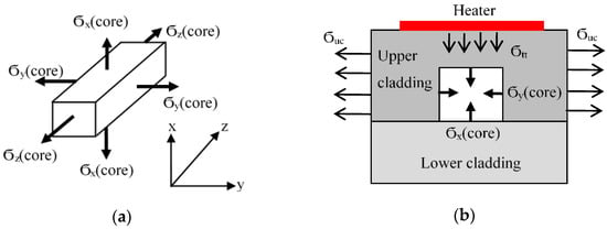
Figure 1.
Schematic distribution of the stress field vectors and the thermal field vector for a silica waveguide channel: (a) the perspective view; (b) the cross-sectional view.
In Figure 1, , , and are the components of the stress tensor in the x-, y-, and z- directions, respectively; represents the stress in the upper cladding layer; and is the thermal stress generated by the heater during heat conduction. Thus, the deposited film stress causes the entire birefringence of the film, which can define the refractive index change in the x- and y-directions caused by the film stress. Namely, for the transverse electric mode (TE-mode) and transverse magnetic mode (TM-mode), the stress will produce different changes in the film refractive index. The change values are defined by Equations (1) and (2) below [21]:
where and are stress-optical constants (also called elastic constants), which are determined by Young’s modulus, Poisson’s ratio, and the stress tensor of the material. and are photoelastic tensor elements; then, and can be defined by Equations (3) and (4):
For silica glass materials, the two stress-optical constants are = 0.74 × 10⁻⁵ mm2/kg and = 4.10 × 10⁻⁵ mm2/kg.
In the SiO2 optical waveguide devices, the waveguide structures are generally squared, and the thickness of the upper cladding layer and the pitch of the waveguide channels are much larger than the geometry of the waveguide core layer. Therefore, the orthogonal terms in the elements of the stress density tensor are equal, wherein the symmetric non-orthogonal terms are equal. In addition, the upper cladding layer and the core layer of the waveguide are formed by different deposition amounts but with the same deposition technique and the same procedure; therefore, they have almost the same Young’s modulus and Poisson’s ratio, that is, and . The coefficient of thermal expansion (CTE) of the upper cladding layer, the core layer, and the substrate are , , and , respectively. By referring to Huang’s theoretical model on the distributions and interactions of all the stress fields in the channel waveguide [7], for a temperature difference , the thermal stresses in the x- and y-directions are defined by Equations (5) and (6), respectively:
Among them, determining the stress difference of the waveguide core layer between two directions is called biaxial stress, which can be obtained from the Equations (5) and (6):
At the same time, the stress in the z-direction is defined by Equation (8):
From the above relationship, the stress variation of the waveguide core layer in different directions can be obtained, and further results in the birefringence effect in the waveguide core layer. Therefore, generally, only Equation (7) is used for discussing the birefringence.
For the growth-caused stress of a SiO2 film, Chason’s theoretical model is an effective combination of tensile stress and is expressed by [15]:
with the definitions as
where is the time interval from the last sublayer to this grain-formed sublayer, is the energy difference between the surface and grain boundary, is the grain size, is a constant depending on the deposition condition, is the increase in chemical potential of the surface because the film is not in equilibrium during deposition, is the volume associated with adding an atom to the grain boundary, is an effective diffusivity related to the rate of hopping from the surface into the triple junction, is the normal size of the atom (same as the sublayer spacing), is the Boltzmann constant, is the absolute temperature, is the biaxial modulus of the i’th sublayer of film, and is a dimensionless concentration (fractional coverage) of mobile atoms on the surface that are free to make diffusive jumps into the triple junction.
For the structural stress of a SiO2 film, our theoretical model is based on the interactions among all the layers and the interaction in any layer is dependent on the radius on the wafer defined by [14]:
where is the elastic modulus of the finished film, is the elastic modulus of the j’th sublayer material, and are the thickness of the j’th sublayer and the total thickness of the film configuration, respectively. At the condition of , we assume the individual sublayer to be unstrained with a relaxed length of after being deposited, the neutral thickness defined by:
where and are the Poisson ratios of the substrate and i’th sublayer of film, respectively. In Equation (15), the curvature should be variable with radius , so it is theoretically determined by the multilayered configuration with the elastic modulus of each sublayer as
where is a parameter for adjusting the relations between the strain and stress of all sublayers after the i’th sublayer is deposited, which is defined by
with the definition as that is −1 for , 0 for , and 1 for , and the elastic modulus is also transferred to the effective modulus by the total widths of the i’th sublayer and bottom layer: and as
in Equations (13) and (14), both and are the functions of radius , so the key parameters and are certainly the functions of . Therefore, from the definition model Equation (14) of the structural stress of film, is confirmed to be a function of .
3. Results and Discussion
3.1. Numerical Calculations
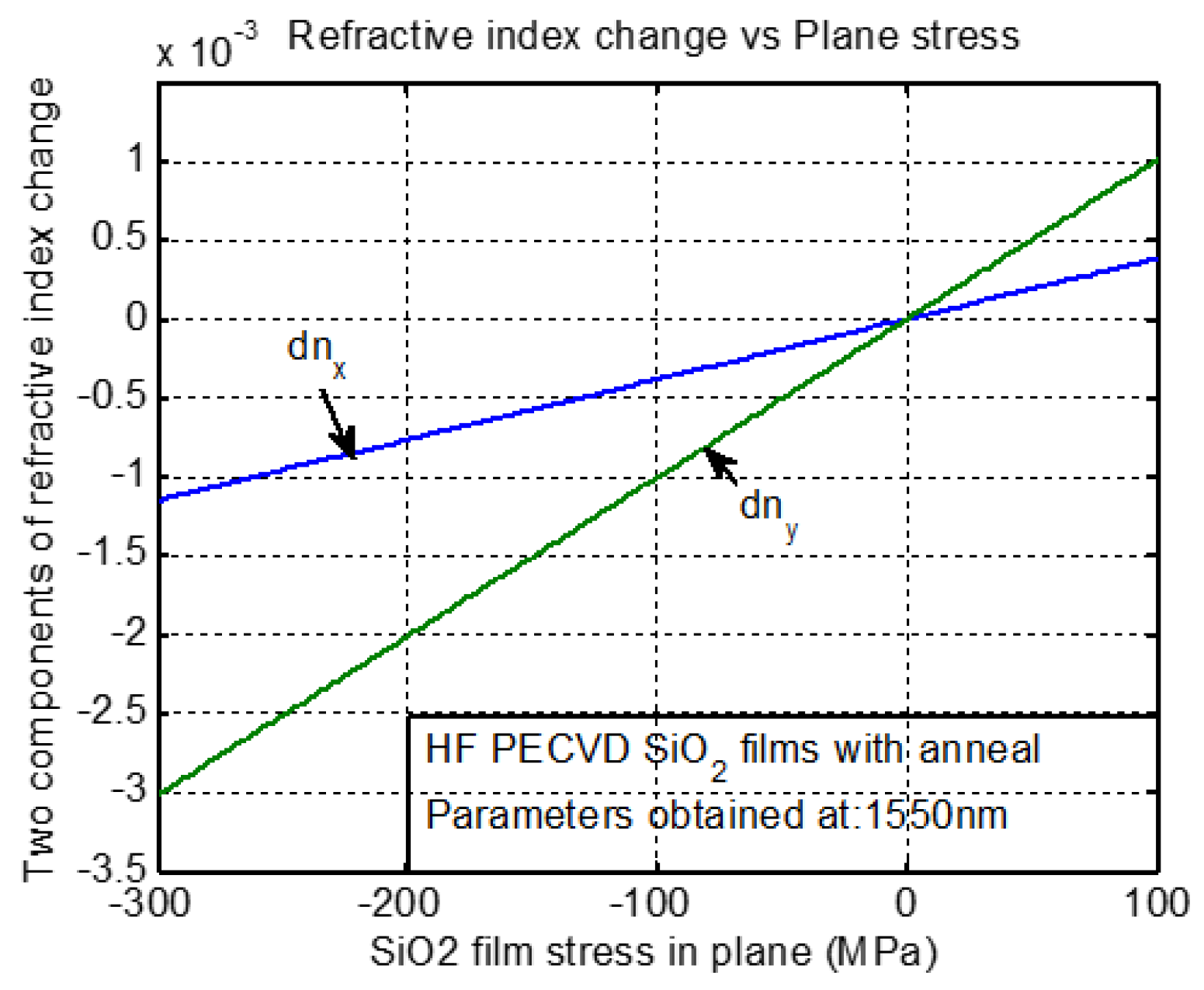
Using Equations (1) and (2) together with Equations (3) and (4), the refractive index changes with the source stress of the film are numerically calculated as shown in Figure 2. Therefore, with the difference between and in Figure 2, the corresponding stress value can be obtained and then at a wavelength of 1550 nm, the relationship between the film stress and the birefringence is numerically simulated. Note from Figure 2 that the simulation curves of the stress-optical constants and have an interaction. Therefore, it was concluded that the relative amplitudes of these two constants can not only determine the final stress value of a film but also control the stress property, the tensile stress, or the compress stress.
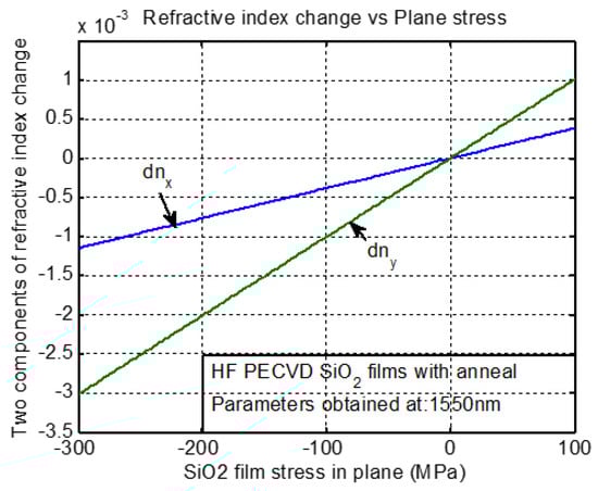
Figure 2.
Relationship between birefringence and film stress at a wavelength of 1550 nm.
For the thermal stress that is caused by the temperature difference between the inside and outside temperatures of the coating chamber, when the film stress was ± 100 MPa, was ±4.0 × 10⁻⁴ and was ±10.10 × 10⁻⁴. According to the above definition of the refractive index ellipsoidal coordinates in the TEM mode light wave condition, and were caused by a change of and , respectively, causing a value of ±6.0 × 10⁻⁴ birefringence.
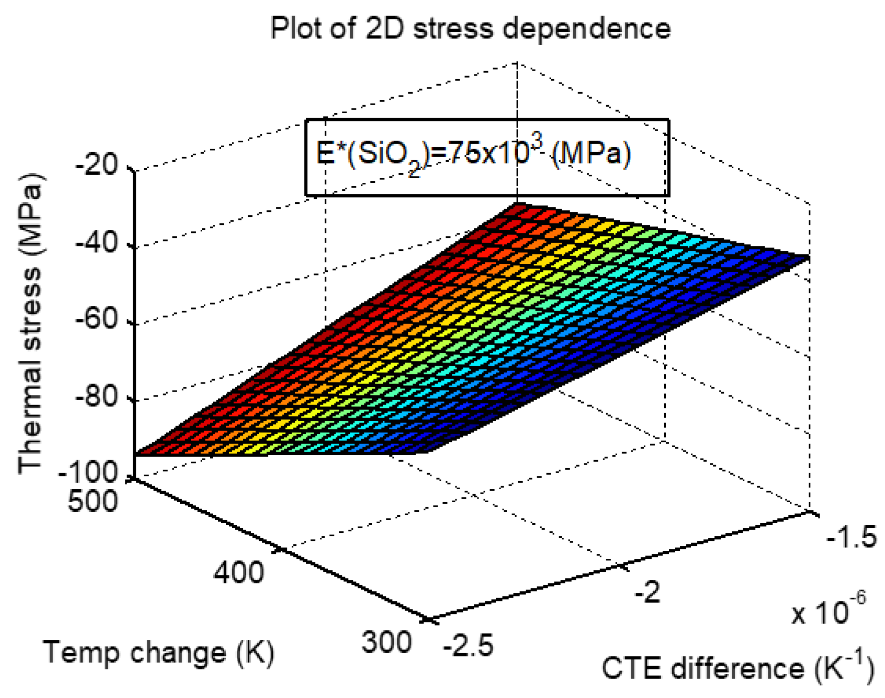
To compare the thermal stress with the total intrinsic stress of the thin films deposited by PECVD, it is mandatory to first investigate the thermal stress dependence on the two dominant factors of Equation (7): and . By assuming that is from −1.5 × 10⁻⁶ to −2.5 × 10⁻⁶ (1/°C) and is from 300 to 500 °C—the biggest temperature range in the PECVD deposition of SiO2 films—with Equations (7) and (8) we numerically simulated the thermal stress dependence on and , then obtained the 2D distribution as shown in Figure 3. Note that first the thermal stress was the compress stress and at tens of MPa, but was much lower than the measured values of the final residual stress. Then, the CTE and the temperature had equal influence on the thermal stress; namely, both and linearly affected the thermal stress. In addition, in this simulation, as the stress was assumed to be uniform over the wafer, it could not accurately express the stress distribution. For the simulation results shown in Figure 3, what needs to be clarified is that the temperature for a PECVD deposition operation is generally controlled in a stable range; namely, the does not have a big change, but the CTE has a relatively big change depending on the deposition conditions. Therefore, the thermal stress was contributed mainly by .
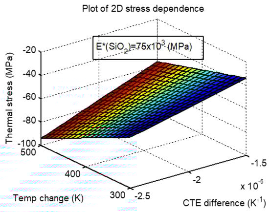
Figure 3.
Numerical simulation results of the 2D thermal stress distribution with both the coefficient of thermal expansion (CTE) difference and temperature change in which the biaxial elastic modulus is taken as E*(SiO2) = 75 × 103 (MPa).
It turns out that the thermal stress defined by Equations (7) and (8) is based on only one intrinsic stress source, the thermal stress, rather than the total stress of the film. For the general case, = 2.6 × 10⁻⁶ (1/K) and = 0.5 × 10⁻⁶ (1/K), and the = 400 °C, the thermal stress value is −64.8 MPa. In fact, the structural stress is an extra stress imposed on the sum of the two intrinsic stresses, the growth-caused stress and the thermal stress.
With Equations (9) and (10), we numerically simulated the dependence of growth-caused stress on both the growth rate and the normalized size of an atom and then obtained the 2D distribution as shown in Figure 4. Note that the growing technique and conditions, including the selection of the key parameters in the coating process, have an important influence on the final growth stress, which can be used to conserve the other stresses. In addition, the growth-caused stress increases with both the growth rate and the atom size.
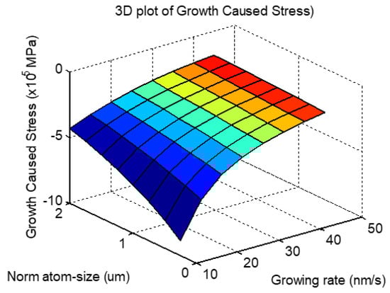
Figure 4.
Numerical simulations for the growth-caused stress of SiO2 film vs. both the growth rate and normalized atom size, where the parameters used in the simulations are set as: = 6.0 μm, = 6.0 μm, = 0.117 × 10⁻¹⁵ m2/s, = 0.13 J, = 0.13 × 10⁻⁶ V.
In the same manner, with Equations (11)–(15), we numerically simulated the dependence of the structural stress of a SiO2 film on a 6-inch 625 μm-thick silicon wafer on the measured radius and film thickness, and then obtained the 2D distribution as shown in Figure 5. Note that from the center to the edge, the film’s structural stress increased nonlinearly with both the measured radius and the film thickness, which matches exactly with the inverse nonlinear distribution of the growth-caused stress.
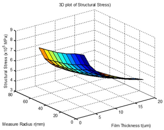
Figure 5.
Numerical simulation for the dependences of the structural stress of SiO2 film on both the measured radius and the thickness.
For analyzing the waveguide channel structure and stress distribution shown in Figure 1a, we fabricated the samples of waveguides and then measured the distribution of stress and birefringence with a prism coupler Metricon-2010 (Pennington, NY, USA). The measured results of surface quality, numerical simulation, and experiments had the same trend.
3.2. Experimental Measurements
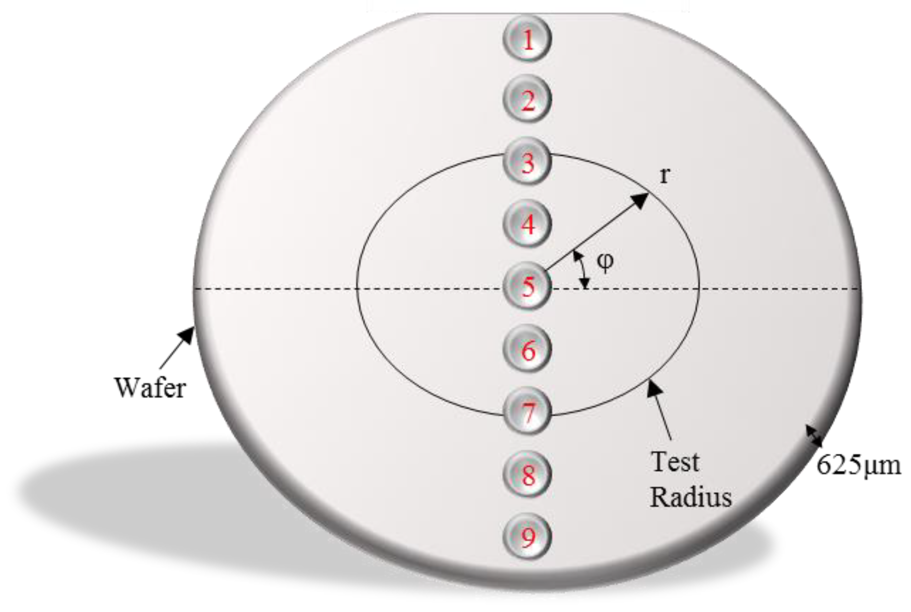
In the deposition process of a SiO2 film with a 6 μm thickness, with the prism coupler Metricon-2010 and at a wavelength of = 1539 nm, a 9-point test method was exploited to measure the birefringence values as shown in Figure 6, in which point 5 is the center and points 1 and 9 are the edges of the silicon wafer. The refractive index and birefringence distribution on a 6-inch silicon wafer under typical deposition conditions were systematically measured: deposition pressure, power, gas flow ratio, substrate temperature, and annealing conditions. Using the measurement results of birefringence (), the stress distribution of the SiO2 film from the center to the edge of the entire wafer was calculated systematically.
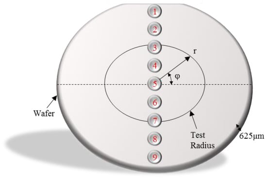
Figure 6.
Selected positions for birefringence distribution measurements across the wafer.
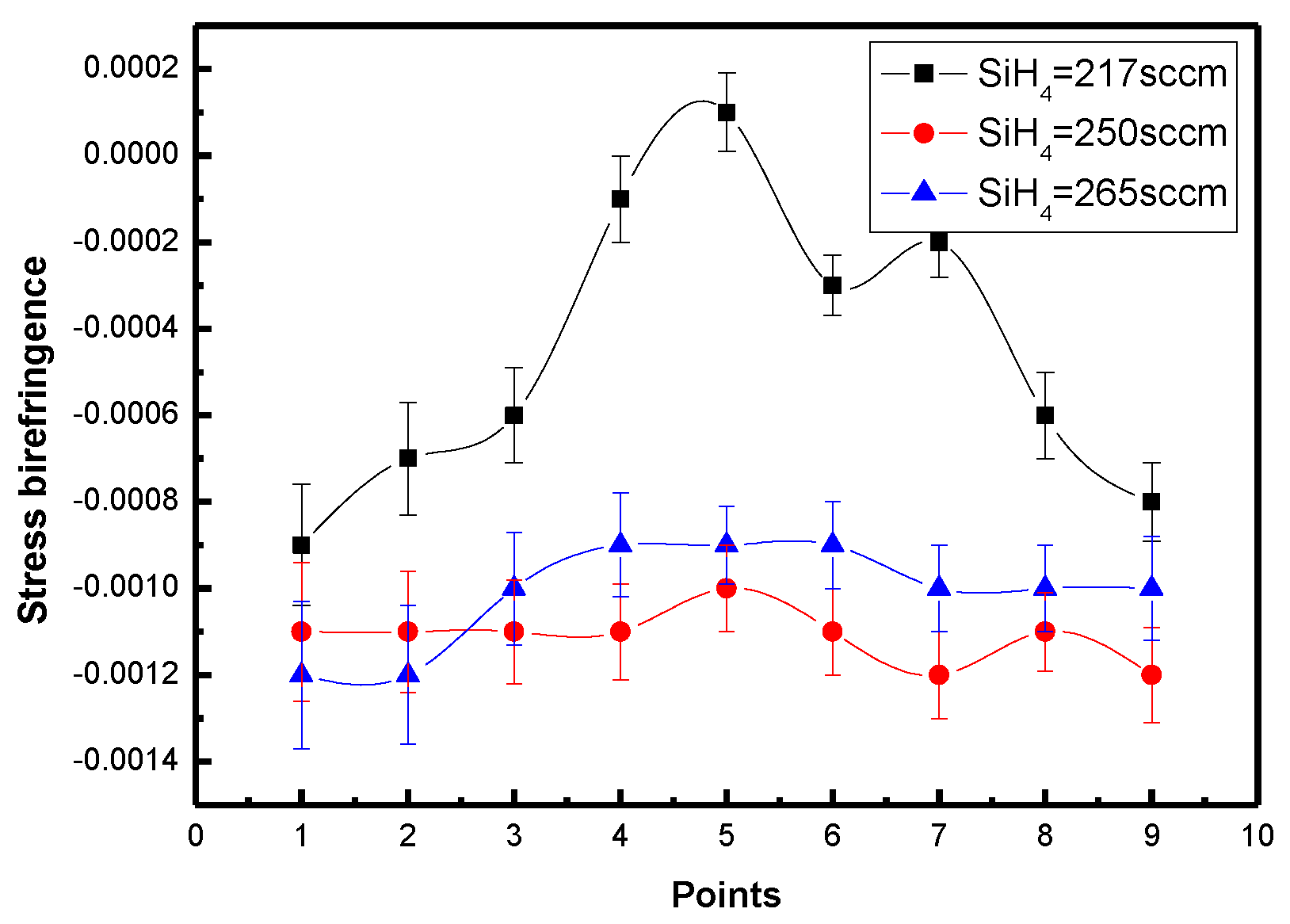
In experiments, a 6-inch silicon wafer with a 6-μm-thick SiO2 film was subjected to stress measurement with a circular coordinate as a radius and an angle as shown in Figure 6. The deposition conditions were set as SiH4: N20 = 200:6000, the doping flow of the GeH4 gas was 50 sccm, the substrate temperature was 400 °C, and the RF power was 1000 W. For three 6 μm-thick film samples deposited at SiH4 gas flow rates of 217, 250, and 265 sccm, we measured the values with the prism coupler Metricon-2010 at a wavelength = 1539 nm. Then, we obtained the corresponding birefringence distributions with respect to the three SiH4 gas flow rates, shown in Figure 7. It can be noticed that apparently variable stress distributions from the center to the edge of the wafer for all three SiH4 gas flow rates were formed. The birefringence of the wafer edge was higher than the center for the flow rate of SiH4 to be 217 sccm. However, when this flow rate was increased to 250 sccm, the distribution variability was gradually weakened, while the amplitude of the directional stress increased uniformly. It almost did not increase further when this flow rate was increased to 265 sccm and approached a more stable state. In addition, it can also be found that when the SiH4 flow rate was at a level of 217 sccm after doping with GeH4 gas, the stress value changed from a positive value at the wafer center to a negative value at the wafer edge; that is, the reverse stress changes the stress of the entire wafer, which is called reverse pull in the industry.
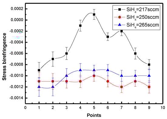
Figure 7.
Birefringence distribution of SiO2 film after doping with GeH4 gas.
Then, from Figure 7, three birefringence values were selected as listed in Table 1. Note that the birefringence maintains uniformity in a large area from the center to the half-radius, but it became much higher in the edge region than the large intermediate region. Further, with the and values of 0.74 × 10⁻⁵ and 4.10 × 10⁻⁵ (mm2/kg), respectively, the corresponding stress values were obtained as depicted in Table 2. Note from Table 2 that the experimental results of the stress at the areas from the center to the middle was about 250 MPa (1 kgf/mm2 = 9.8 MPa), while it was over 1000 MPa at the edge of the wafer.

Table 1.
Measured values of birefringence for the wafer.
Table 2.
Calculated values of stress with the measured birefringence.
In summary, the amplitude of the measured negative stress was much higher than the uniform negative thermal stress shown in Figure 3, which was around −60MPa, but was much lower than both the growth stress shown in Figure 4, which was negative 4–6 × 10⁵ MPa, and the structural stress shown in Figure 5, which was positive 4–6 × 10⁵ MPa. Therefore, the algebraic sum of these two stresses (growth stress and structural stress) are only agreeable with the nonuniform measured values.
4. Conclusions
For the silica waveguide-based PLC chip products, it is unavoidable that a deformation occurs when depositing a SiO2 film on a large wafer by PECVD. Therefore, in this article, the birefringence distribution of the SiO2 film on a 6-inch Si wafer was investigated in both theory and experiments. The corresponding stress values were further calculated to confirm the main factors affecting the optical property uniformity of the film. The findings of the nonuniform birefringence distributions are very sustainable for enhancing the yields of the silica waveguide-based PLC chip products.
Author Contributions
Conceptualization, Q.S. and D.S.; methodology, H.S., T.Y. and L.C.; validation, D.S.; formal analysis, D.S.; investigation, T.Y. and M.D.; data curation, Q.S., H.S. and Z.S; writing—original draft preparation, Q.S.; writing—review and editing, D.S.; visualization, Z.S. and W.X.
Funding
This work is co-sponsored by the Natural Science Foundation of Jilin Provincial Science & Technology (Foundation Grant: 20180101223JC) and the Innovative R&D Fund / Education Fund of CUST, the invest of D&T Photonics, a startup spun-off from University of Ottawa, Canada, and the Fundamental/in-kind invests of Sino-Electronics Corporation.
Acknowledgments
The authors thank the Jilin Sino Microelectronics, Ltd Corporation for their help in PECVD coatings of wafer samples. The authors would like to thank Prof. Wang Guozheng of the School of Science at the CUST, China, for his help in wafer processing, Wang Xueping, a graduate, for her support in testing the optical performance of the SiO2 films, and Prof. Weng Zhankun of the International Research Centre for Nano Handling and Manufacturing at the CUST, China, for providing the testing equipment.
Conflicts of Interest
The authors declare no conflict of interest.
References
- Doerr, C.R.; Okamoto, K. Optical Fiber Telecommunications V A; Academic Press/Elsevier: New York, NY, USA, 2008; pp. 269–341. [Google Scholar]
- Wu, X.P.; Liu, W.; Yuan, Z.L.; Liang, X.R.; Chen, H.; Xu, X.H.; Tang, F.F. Low power consumption VOA array with air trenches and curved waveguide. IEEE Photon. J. 2018, 10, 7201308. [Google Scholar] [CrossRef]
- Wang, J.; Yi, J.; Guo, L.J.; Liu, P.; Hall, T.J.; Sun, D.G. Improved silica-PLC MZI type optical switches with error dependence compensation of directional coupler. Opt. Las Technol. 2017, 89, 208–213. [Google Scholar] [CrossRef]
- Okamoto, K. Planar Lightwave Circuits (PLCs). In Fundamentals of Optical Waveguides, 1st ed.; Academic Press: New York, NY, USA, 2000; pp. 341–400. [Google Scholar]
- Tomlinson, W. Evolution of passive optical component technologies for fiber-optic communication systems. J. Lightwave Technol. 2008, 26, 1046–1063. [Google Scholar] [CrossRef]
- Takato, N.; Jinguiji, K.; Yasu, M.; Toba, H.; Kawachi, M. Silica-based single-mode waveguides on silicon and their application to guided-wave optical interferometers. J. Lightwave Technol. 1988, 6, 1003–1010. [Google Scholar] [CrossRef]
- Huang, M. Analytical solutions for thermal stress in buried channel waveguides on silicon and their application to guided-wave optical interferometers. IEEE J. Quantum Electron. 2004, 40, 1562–1568. [Google Scholar] [CrossRef]
- Guan, D.; Bruccoleri, A.R.; Heilmann, R.K.; Schattenburg, M.L. Stress control of plasma enhanced chemical vapor deposited silicon dioxide from tetraethoxysilane. J. Micfromech. Microeng. 2013, 24, 027001. [Google Scholar] [CrossRef]
- Wu, F.; Lagally, M.G. Ge-induced reversal of surface stress anisotropy on Si (001). Phys. Rev. Lett. 1995, 75, 2534–2537. [Google Scholar] [CrossRef] [PubMed]
- Chen, J.; Wolf, I.D. Study of damage and stress induced by backgrinding in Si wafers. Semicond. Sci. Technol. 2003, 18, 261–268. [Google Scholar] [CrossRef]
- Yao, Y.W.; Chalifoux, B.D.; Heilmann, R.K.; Schattenburg, M.L. Thermal oxide patterning method for compensating coating stress in silicon substrates. Opt. Express. 2019, 27, 1010–1025. [Google Scholar] [CrossRef] [PubMed]
- Chen, K.S.; Zhang, X.; Lin, S.Y. Intrinsic stress generation and relaxation deposited oxide during deposition and subsequent thermal cycling. Thin Solid Films. 2003, 434, 190–202. [Google Scholar] [CrossRef]
- Chason, E.; Shin, J.W.; Hearne, S.J.; Freund, L.B. Kinetic model for dependence of thin film stress on growth rate, temperature, and microstructure. J. Appl. Phys. 2012, 111, 083520. [Google Scholar] [CrossRef]
- Sun, D.G.; Sun, Q.Y.; Xing, W.C.; Sun, Z.Y.; Shang, H.P.; Chang, L.Y.; Wang, X.P.; Liu, P.; Hall, T.J. Investigation for the structural stress of SiO2 thin films and its distribution on the large-wafer created by plasma enhanced chemical vapor deposition. AIP Adv. 2018, 8, 085217. [Google Scholar] [CrossRef]
- Watanabe, K.; Kasahama, R.; Hashizume, Y. Extremely-low-power-consumption Thermo-optic Switch with silicon-silica hybrid structure. NTT Technol. Rev. 2010, 8, 1–5. [Google Scholar]
- Morinaki, O.; Noguchi, K.; Takahashi, H.; Sakamoto, T.; Sato, K.I.; Hasegawa, H.; Okuno, M.; Ohmori, Y. Multihop signal transmission experiments employing PLC-based hierarchical optical cross-connect system. IEEE Photon. Technol. Lett. 2010, 22, 1586–1588. [Google Scholar] [CrossRef]
- Watanabe, T.; Suzuki, K.; Takahashi, T. Silica-based PLC transponder aggregators for colorless, directionless, and contentionless ROADM. In Proceedings of the Optical Fiber Communication Conference & Exposition, OSA Technical Digest (OSA, 2012), LA, CA, USA, 4–8 March 2012. Paper OTh3D.1. [Google Scholar]
- Choi, J.K.; Lee, J.; Yoo, J.B.; Maeng, J.S.; Kim, Y.M. Residual stress analysis of SiO2 films deposited by plasma-enhanced chemical vapor deposition. Surf. Coat. Technol. 2000, 131, 153–157. [Google Scholar] [CrossRef]
- Okuno, M.; Sugita, A.; Jinguli, K.; Kawachi, M. Birefringence control of silica waveguides on Si and its application to polarization beam splitter/switch. J. Lightwave Technol. 1994, 12, 625–633. [Google Scholar] [CrossRef]
- Zhao, X.; Xu, Y.Z.; Li, C. Birefringence control in optical planar waveguides. J. Lightwave Technol. 2003, 21, 2352–2356. [Google Scholar] [CrossRef]
- Ye, W.N.; Xu, D.X.; Janz, S.; Cheben, P.; Picard, M.J.; Lamontagne, B.; Tarr, N.G. Birefringence control using stress engineering in silicon-on-insulator (SOI) waveguides. J. Lightwave Technol. 2005, 23, 1308–1318. [Google Scholar] [CrossRef]


© 2019 by the authors. Licensee MDPI, Basel, Switzerland. This article is an open access article distributed under the terms and conditions of the Creative Commons Attribution (CC BY) license (http://creativecommons.org/licenses/by/4.0/).