Surface Morphology of Silicon Waveguide after Reactive Ion Etching (RIE)


Abstract
:1. Introduction
2. Experimental Approach
3. Results and Discussion
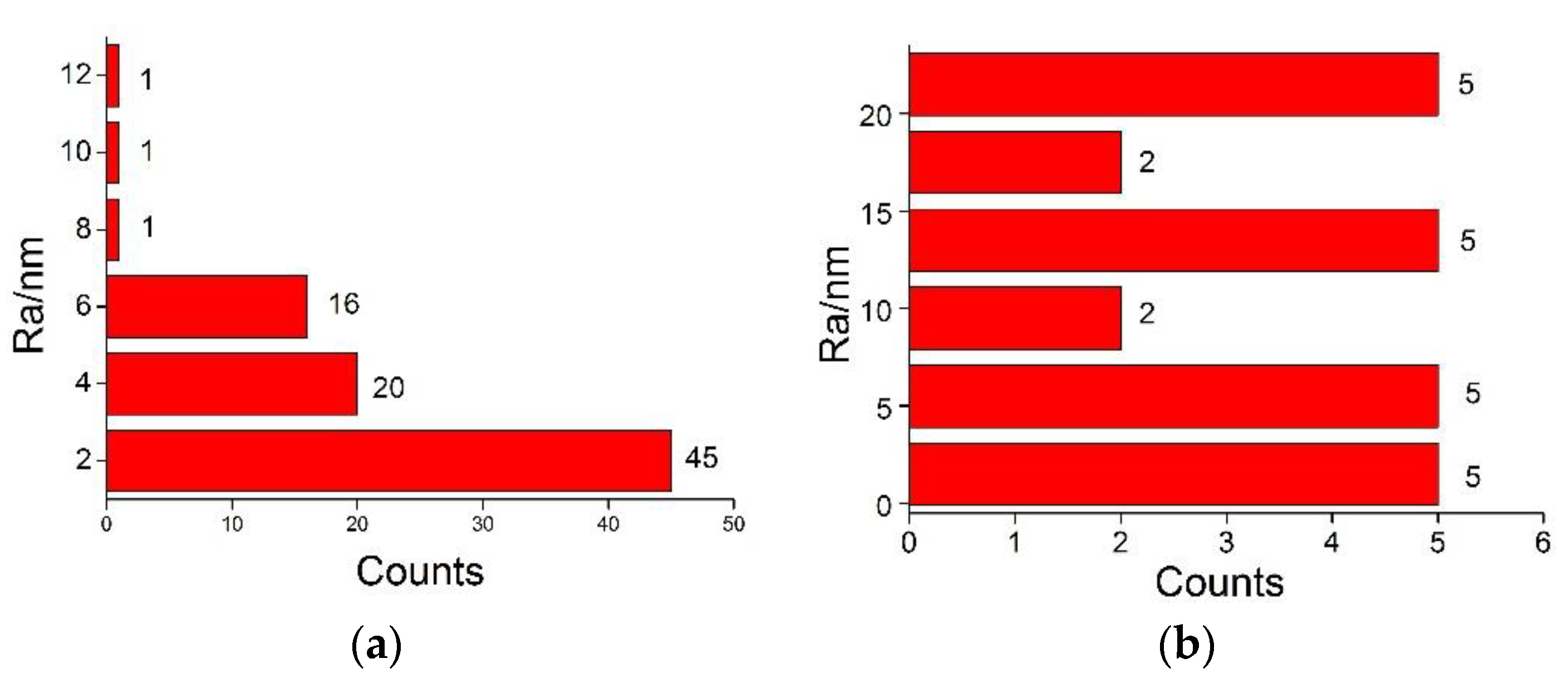
3.1. 2-D Side Wall Roughness
3.1.1. Before Reactive Ion Etching
3.1.2. After Reactive Ion Etching
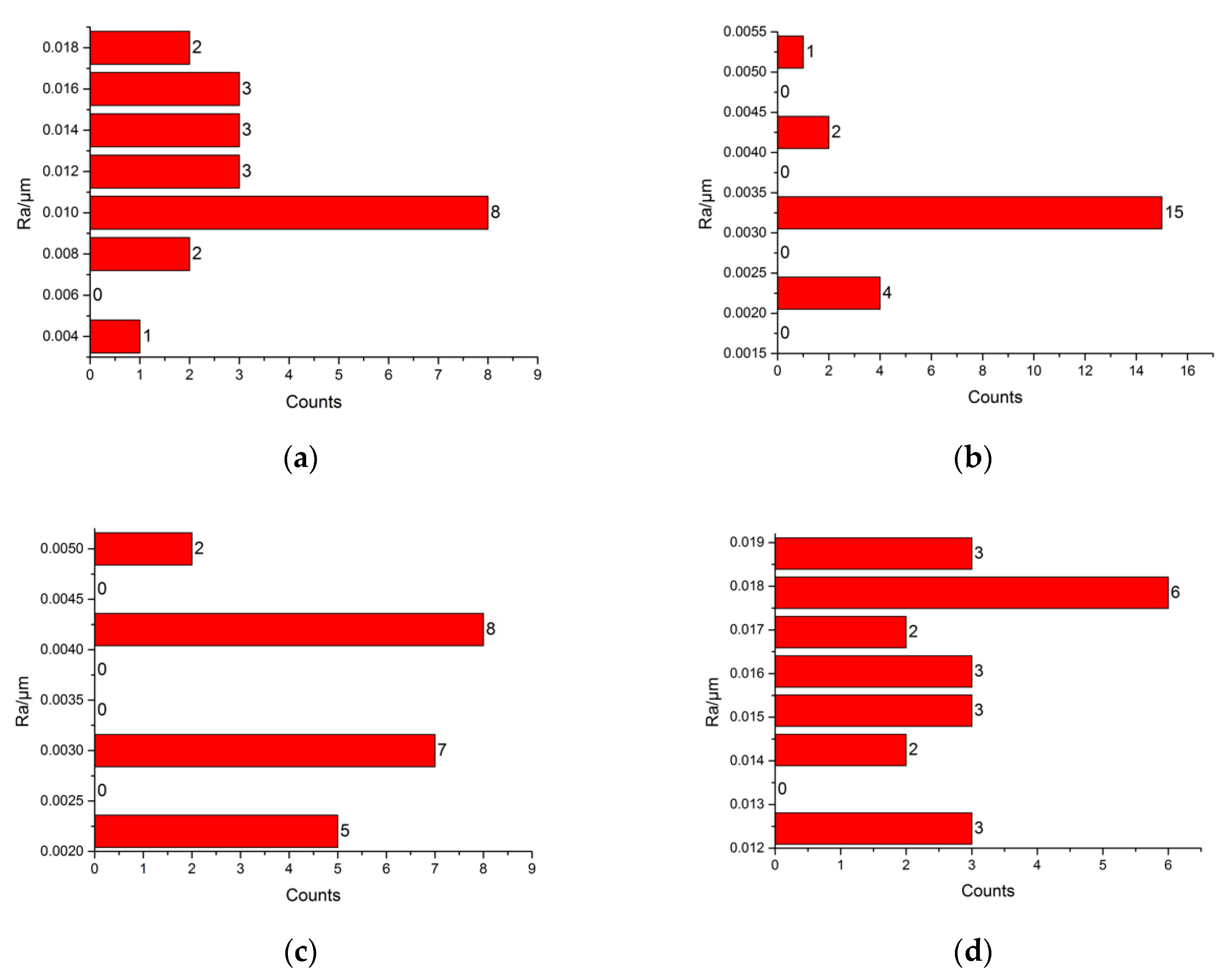
3.2. Bottom Roughness
4. Conclusions
Author Contributions
Funding
Conflicts of Interest
References
- Meister, S.; Franke, B.; Eichler, H.J.; Kupijai, S.; Rhee, H.; Al-Saadi, A.W.S.; Zimmermann, L. Photonic Integrated Circuits for Optical Communication. Opt. Photonik 2012, 7, 59–62. [Google Scholar] [CrossRef] [Green Version]
- Doerr, C. Silicon photonic integration in telecommunications. Front. Phys. 2015, 3, 137–179. [Google Scholar] [CrossRef]
- Vahala, K.J. Optical microcavities. Nature 2003, 424, 839. [Google Scholar] [CrossRef] [PubMed]
- Chen, X.; Li, C.; Tsang, H.K. Device engineering for silicon photonics. NPG Asia Mater. 2011, 3, 34–40. [Google Scholar] [CrossRef] [Green Version]
- Dai, D.; Bauters, J.; Bowers, J.E. Passive technologies for future large-scale photonic integrated circuits on silicon: Polarization handling, light non-reciprocity and loss reduction. Light Sci. Appl. 2012, 1, 500–505. [Google Scholar] [CrossRef]
- Rahman, M.S.B.A.; Ater, F.S.S.; Mohammad, R. Effects of random sidewall roughness on optical power splitter. Opt. Eng. 2015, 54, 055103. [Google Scholar] [CrossRef]
- Barwicz, T.; Haus, H.A. Three-Dimensional Analysis of Scattering Losses Due to Sidewall Roughness in Microphotonic Waveguides. J. Lightwave Technol. 2005, 23, 2719–2732. [Google Scholar] [CrossRef]
- Gnan, M.; Thoms, S.; Macintyre, D.S.; De La Rue, R.M.; Sorel, M. Fabrication of low-loss photonic wires in silicon-on-insulator using hydrogen silsesquioxane electron-beam resist. Electron. Lett. 2008, 44, 115. [Google Scholar] [CrossRef]
- Lee, K.K.; Lim, D.R.; Kimerling, L.C.; Shin, J.; Cerrina, F. Fabrication of ultralow-loss Si/SiO2 waveguides by roughness reduction. Opt. Lett. 2001, 26, 1888–1890. [Google Scholar] [CrossRef]
- Binnig, G.; Rohrer, H.; Gerber, C.; Weibel, E. Surface studies by scanning tunneling microscopy. Phys. Rev. Lett. 1982, 49, 57–61. [Google Scholar] [CrossRef]
- Jang, J.H.; Zhao, W.; Bae, J.W.; Selvanathan, D.; Rommel, S.L.; Adesida, I.; Abeles, J.H. Direct measurement of nanoscale sidewall roughness of optical waveguides using an atomic force microscope. Appl. Phys. Lett. 2003, 83, 4116. [Google Scholar] [CrossRef]
- Martin, Y.; Wickramasinghe, H.K. Method for imaging sidewalls by atomic force microscopy. Appl. Phys. Lett. 1994, 64, 2498–2500. [Google Scholar] [CrossRef]
- Hosomi, K.; Shirai, M.; Hiruma, K.; Shigeta, J.; Katsuyama, T. AFM characterization of GaAs/AlGaAs waveguides. IEICE Trans. Electron. 1996, 79, 1579–1585. [Google Scholar]
- Sum, T.C.; Bettiol, A.A.; Seng, H.L.; Kan, J.V.; Watt, F. Direct measurement of proton-beam-written polymer optical waveguide sidewall morphorlogy using an atomic force microscope. Appl. Phys. Lett. 2004, 85, 1398–1400. [Google Scholar] [CrossRef] [Green Version]
- Pandraud, G.; Margallobalbas, E.; Yang, C.K.; French, P.J. experimental characterization of roughness induced scattering losses in PECVD SiC waveguides. J. Lightwave Technol. 2011, 29, 744–749. [Google Scholar] [CrossRef]
- Pani, S.K.; Wong, C.C.; Sudharsanam, K.; Lim, V. Direct measurement of sidewall roughness of polymeric optical waveguides. Appl. Surf. Sci. 2005, 239, 445–450. [Google Scholar] [CrossRef]
- Gonzalez, R.C.; Woods, R.E.; Eddins, S.L. Digital Image Processing Using MATLAB; Prentice-Hall: Upper Saddle River, NJ, USA, 2003. [Google Scholar]
- Zhang, H.; Li, T.; Jian, A.; Sang, S.; Xue, C.; Zhang, W. Modeling and simulation of the effect of surface roughness on properties of silicon-on-insulator optical ring resonator coupled with a straight waveguide. Opt. Eng. 2015, 54, 125101. [Google Scholar] [CrossRef]
- Sparacin, D.K.; Spector, S.J.; Kimerling, L.C. Silicon waveguide sidewall smoothing by wet chemical oxidation. J. Lightwave Technol. 2005, 23, 2455–2461. [Google Scholar] [CrossRef]
- Shi, Z.; Shao, S.; Wang, Y. Improved the surface roughness of silicon nanophotonic devices by thermal oxidation method. J. Phys. Conf. Ser. 2011, 276, 012087. [Google Scholar] [CrossRef]
- Kuribayashi, H.; Gotoh, M.; Hiruta, R. Observation of Si(1 0 0) surfaces annealed in hydrogen gas ambient by scanning tunneling microscopy. Appl. Surf. Sci. 2006, 252, 5275–5278. [Google Scholar] [CrossRef]
- Armani, D.K.; Kippenberg, T.J.; Spillane, S.M. Ultra-high-Q toroid microcavity on a chip. Nature 2003, 421, 925–928. [Google Scholar] [CrossRef]
- Zhu, X.P.; Suematsu, H.; Jiang, W.; Yatsui, K.; Lei, M.K. Pulsed-ion-beam nitriding and smoothing of titanium surface in a vacuum. Appl. Phys. Lett. 2005, 87, 093111. [Google Scholar] [CrossRef]


| EBL Parameters | RIE Parameters | ||
|---|---|---|---|
| Sample dimension | 15 mm by 15 mm | RF power | 100 W |
| Photoresist | Thickness: 400 nm | SF6 flux | 36 sccm |
| Acceleration voltage | 50 keV | O2 flux | 6 sccm |
| Exposure dose | 300 μ C/cm2 | Gas pressure | 25 Pa |
| development | 4 methyl 2-pentanone soak for 100 s | Temperature | 25 °C |
| fixation | Isopropyl alcohol soak for 30 s | DC bias | 50 V |
| Roughness (nm) | ||||
|---|---|---|---|---|
| Average | Maximum | Minimum | Standard Deviation | |
| Sample 1 | 11.55 | 18 | 4 | 3.38 |
| Sample 2 | 3 | 5 | 2 | 0.69 |
| Sample 3 | 3.32 | 5 | 2 | 0.945 |
| Sample 4 | 16.18 | 19 | 12 | 2.3 |
© 2019 by the authors. Licensee MDPI, Basel, Switzerland. This article is an open access article distributed under the terms and conditions of the Creative Commons Attribution (CC BY) license (http://creativecommons.org/licenses/by/4.0/).
Share and Cite
Zheng, Y.; Gao, P.; Jiang, L.; Kai, X.; Duan, J. Surface Morphology of Silicon Waveguide after Reactive Ion Etching (RIE). Coatings 2019, 9, 478. https://doi.org/10.3390/coatings9080478
Zheng Y, Gao P, Jiang L, Kai X, Duan J. Surface Morphology of Silicon Waveguide after Reactive Ion Etching (RIE). Coatings. 2019; 9(8):478. https://doi.org/10.3390/coatings9080478
Chicago/Turabian StyleZheng, Yu, Piaopiao Gao, Lianqiong Jiang, Xiaochao Kai, and Ji’an Duan. 2019. "Surface Morphology of Silicon Waveguide after Reactive Ion Etching (RIE)" Coatings 9, no. 8: 478. https://doi.org/10.3390/coatings9080478