Abstract
Towards the integration of Digital-LDO regulators in the ultra-low-power System-On-Chip Internet-of-Things architecture, the D-LDO architecture should constitute the main regulator for powering digital and mixed-signal loads including the SoC system clock. Such an implementation requires an in-regulator clock generation unit that provides an autonomous D-LDO design. In contrast to contemporary D-LDO designs that employ ring-oscillator architecture which start-up time is dependent on the oscillating frequency, this work presents a design with nano-power consumption, fabricated with an active area of 0.035 at a 55-nm Global Foundries CMOS process that introduces a fast start-up burst oscillator based on a high-gain stage with wake-up time independent of D-LDO frequency. In combination with linear search coarse regulation and asynchronous fine regulation, it succeeds 558 nA minimum quiescent current with 75 pF, maximum current efficiency of 99.2% and 1.16x power efficiency improvement compared to analog counterpart oriented to SoC-IoT loads.
1. Introduction
With recent advances in System-on-Chip (SoC) architecture in the context of Internet-of-Things (IoT) devices, a need for autonomous devices that can be powered by harvesting the energy from outside sources has arisen [1]. One possibility is to use the query signal as the power source, such as in Ultra-High-Frequency Radio Frequency Identification (UHF-RFID). For these autonomous devices to work with such a low amount of available power, they need highly efficient power management. A key component of such SoC-IoT applications is the Low Drop-Out regulator (LDO). LDOs are DC voltage regulators that regulate the output voltage even when it is close to supply output voltage, which is the case in sub-1 V general IoT [2,3] and passive radio communication systems. In such a system as seen in Figure 1, the power efficiency is maximized with the minimization of the drop-out voltage which is defined as the difference from the rectified voltage to the power line voltage. Conventional Digital-LDO architectures (D-LDO) show-off drop-out voltage as low as 50 at 0.5 regulation voltage that offers a significant advantage compared to analog-LDOs [4] that are incapable of supporting comparable drop-out voltage in ultra-low-power and ultra-low-voltage specifications. In combination with state-of-the-art bandgap voltage references [5,6,7,8] that operate down to 0.5 V opens-up the perspective of operating the system at sub-1 V voltage with high efficiency.
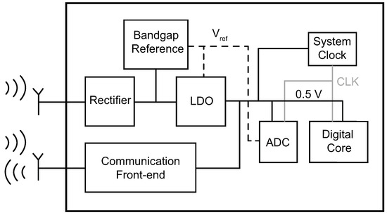
Figure 1.
Passive SoC-IoT system that operates at 0.5 V.
At IoT applications, voltage regulators condition the incoming power from the energy scavenger unit and power digital loads such as the SoC system oscillator. In the prospect of a D-LDO, which constitutes the main regulator at an ultra-low-power IoT system as demonstrated in Figure 1, D-LDO should have an optimized design in order to be independent of external oscillator units such that is able to wake-up and power the system including the system clock. Consequently, the clock generation unit should be included in the D-LDO design. In contrast to conventional D-LDO architectures [9,10,11] as well as the hybrid schemes [12] that are oriented for high efficient regulation at sub-watt applications, there is limited literature available on D-LDO designs applicable to ultra-low power IoT systems by implementing integrated oscillator [13,14,15]. Such integration offers the advantage that coarse and fine regulation is not dependent on the operation of an external clock generation unit. Ring-oscillators are the main architectures that these designs use. A design that employs an integrated ring-oscillator and adapts the sampling frequency across a wide load range has been previously presented [13]. Furthermore, a D-LDO design with event-driven, self-triggering control that has been presented in [14] is based on an architecture that employs an Analog-to-Digital Converter (ADC) with multiple asynchronous comparators, a Proportional-Integrator controller, and burst current-starved ring-oscillator. Additionally, the architecture presented in [15] is based on binary-search coarse regulation and linear search fine regulation supported by an ultra-low frequency ring-oscillator that operates the synchronous fine regulation as well as charge-pump assisted transient comparators. In contrast to the aforementioned designs, this work presents a D-LDO regulator dedicated to ultra-low-power SoC-IoT that introduces an optimized instant pulse clock generation unit based on a high-gain latch stage. This specific configuration provides instant response to load disturbance independent of the D-LDO clock frequency as well as shows off a power efficiency improvement of 1.16x compared to analog-LDO rated for similar IoT loads [4].
2. Proposed Architecture
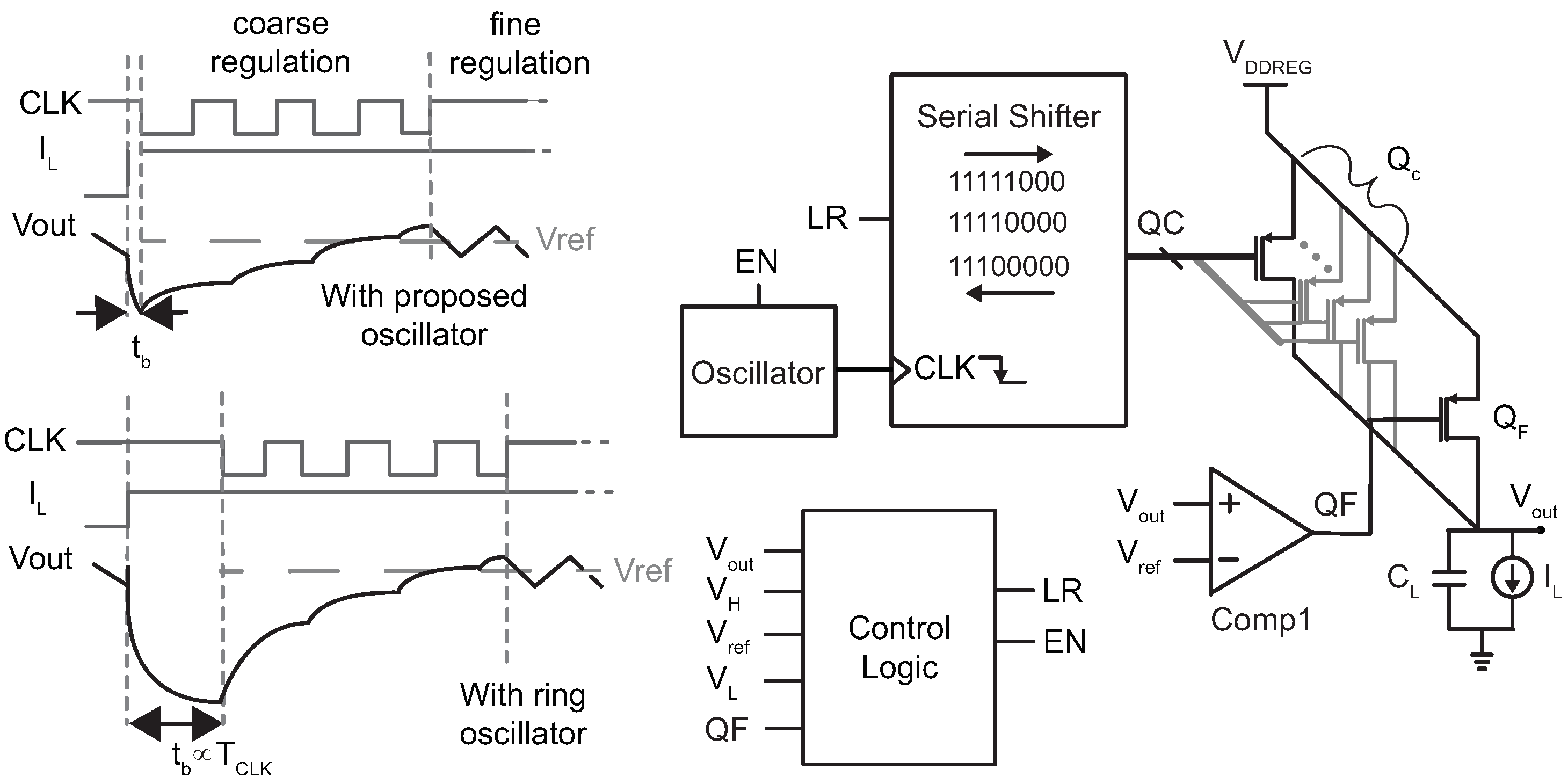
With the purpose to meet the SoC-IoT specifications as described, the proposed D-LDO is designed with fine regulation performed in asynchronous scheme, and synchronous coarse regulation assisted with burst-operated oscillator. Commonly used cold start-up operation of a ring-oscillator relies on charging and discharging of consecutive delay stages [16], thus the burst-clock response naturally depends on the oscillator frequency () as illustrated in Figure 2. In contrast, the presented oscillator is based on a multi-vibrator design assisted by a latched comparator accompanied by an appropriate wake-up circuit which triggers the serial shifter with delay independent of the oscillator frequency. As shown in Figure 2, with the purpose to perform load regulation, the system incorporates the control logic block that controls the current state which is alternated between fine and coarse regulation in case of load surge. The control logic unit produces the EN and LR signals that control the ignition of the oscillator and the direction of serial shifter respectively in the case of coarse regulation, while Comp 1 comparator regulates the load with delay hysteresis under fine regulation. pMOS devices correspond to coarse regulation while pMOS device to fine regulation as operated from Comp 1 comparator.

Figure 2.
D-LDO block diagram and transient response comparison between ring-oscillator and the proposed oscillator.
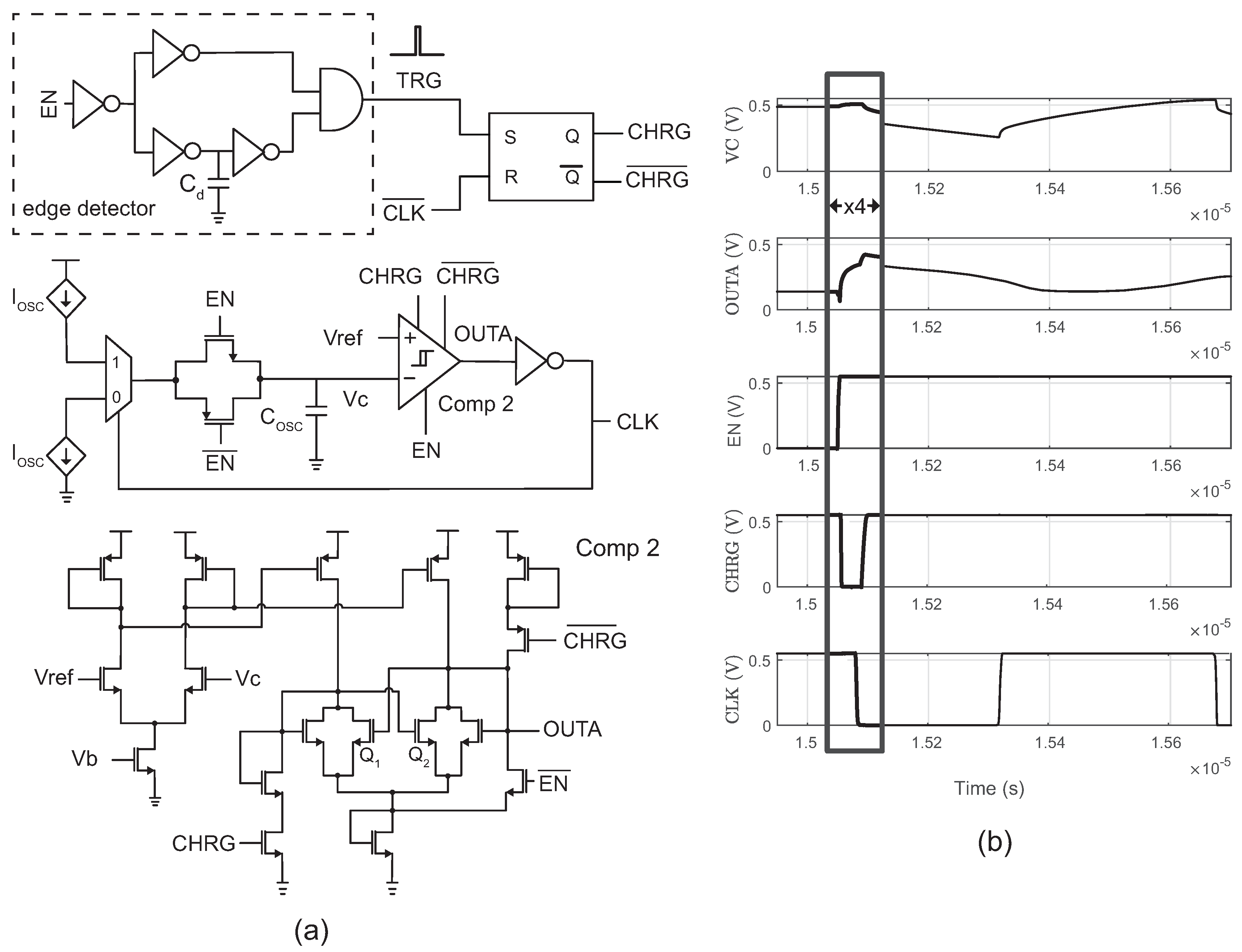
As previously stated, in comparison with current-starved ring-oscillators, a multi-vibrator provided with a latch comparator offers a higher gain with fewer stages consequently, the wake-up process becomes faster. Figure 3a illustrates the oscillator unit that provides the burst-clock generation. While signal EN is set to low, as seen in Figure 3b, at fine regulation, the capacitance is decoupled from the multiplexer. With the purpose to minimize the charge injection into the capacitor a transmission gate is used that holds the signal steady. Meanwhile, the output of the latched comparator Comp 2 is set to low. As EN is pulled up by the control logic when it detects either over-voltage or voltage droop, an edge detector detects the falling edge of the signal and sets the CHRG signal low. The latched comparator is equipped with a branch that sources current to one side of the latch connected to nMOS device and another that drains current from the other side connected to nMOS device , thus the wake-up procedure triggers the latch differentially. As the voltage at the gates of and varies inversely proportional and surpasses differentially the threshold set by certain latch sizing [17], the output OUTA is charged. When the circuitry is latched, the negative edge of CLK output is triggered as well. As the multiplexer selects the current sink, decreases, and the capacitance starts to discharge which means that the oscillations begin. The CHRG signal remains low until the propagation delay of signal set it to high. Therefore, the CHRG signal remains low for a time span irrelevant to the oscillation period. Consequently, burst oscillation responds within time under load current surge that is independent of the oscillator frequency. The oscillation period is defined predominately by the Comp 2 hysteresis levels and , capacitance and parameter as seen in Equation (1).
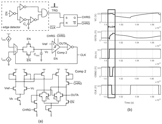
Figure 3.
Schematic (a) and simulation (b) of the oscillator block, designed as a multi-vibrator clock generator with wake-up operation.
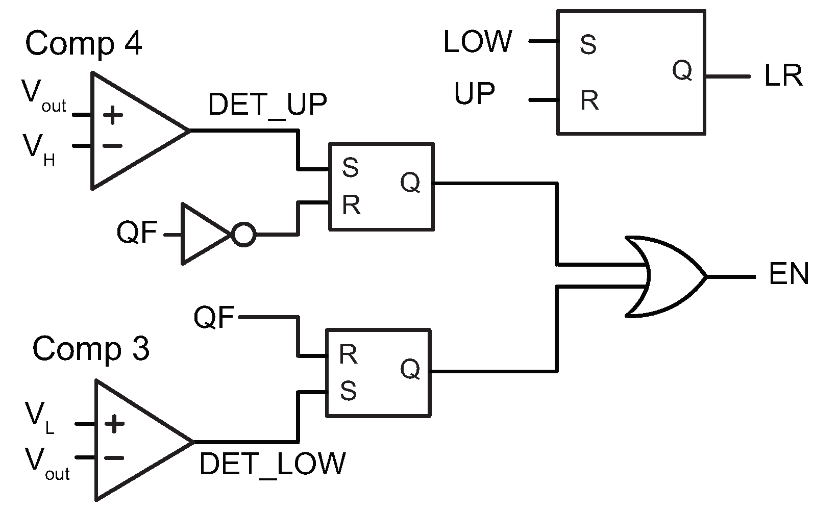
The block diagram of the control logic is illustrated at Figure 4. The comparators Comp 3 and Comp 4 as shown are controlled by voltages and respectively, that define the droop and over-voltage detection thresholds. Each comparator Comp 3 and Comp 4 feeds Set-Reset latches with the signals DET_LOW and DET_UP respectively, and pull up each of them in case of a triggering event. Comparator Comp 1, which is responsible for the hysteretic fine regulation of the output, resets the latches that correspond to Comp 3 and Comp 4 when the coarse regulation converges after a droop or over-voltage recovery. The OR-Gate pulls up the EN signal in case of a droop or over-voltage while EN remains pulled down during fine regulation. The shifting direction is determined through the output of an additional SR latch that is set with the DET_LOW signal and is reset by DET_UP signal. Comp 1 has been implemented as a four-stage comparator that incorporates a differential pair, latch, preamplifier, and a push-pull final stage while Comp 3 and Comp 4 are realized via two-stage latch-based comparators.

Figure 4.
Block diagram of control logic.
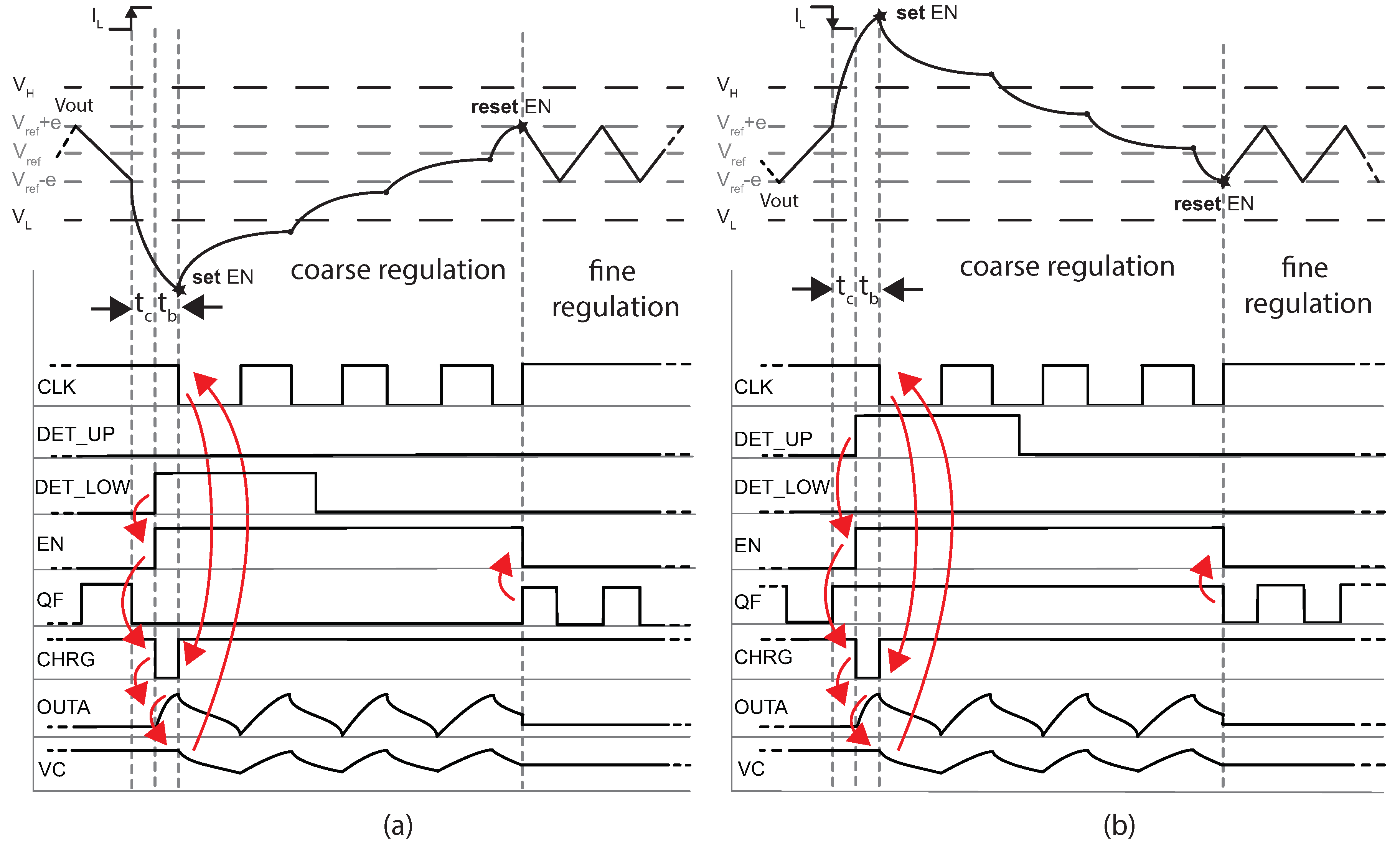
Figure 5 illustrates the detailed timing diagram alongside with the system response under voltage droop and over-voltage. As droop happens in Figure 5a, EN signal is set by DET_LOW and coarse regulation is ignited with CLK negative edge after the delay that depends on the comparator Comp 3 and oscillator start-up delay, and respectively. As seen, after the comparator delay the EN signal is set and output of the comparator Comp2 (OUTA) is charged. As the comparator output surpasses the inverter trip point, the CLK signal is dropped and the oscillations begin soon after where the oscillator wake-up time interval () ends. The CHRG is reset to high state as the clock signal CLK is dropped to LOW. As the clock generation begins, the shift register activates each bit successively and the voltage droop is tamed. When the voltage level is reached, where e is the offset from the reference of the output voltage due to comparison delay, the latch connected to Comp 3 is reset by signal and EN signal is set to low. Since the DET_UP remains low and is low as well, the upper SR latch remains in the previous reset state. That ceases the coarse regulation and fine regulation takes place with ripple magnitude defined merely by the comparison delay of the comparator Comp 3. A similar operation is performed in case of over-voltage as seen in Figure 5b.
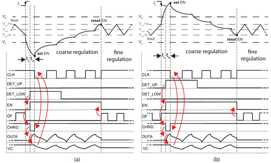
Figure 5.
Conceptual detailed timing diagram of transient response under (a) voltage droop and (b) over-voltage.
3. Implementation and Methodology
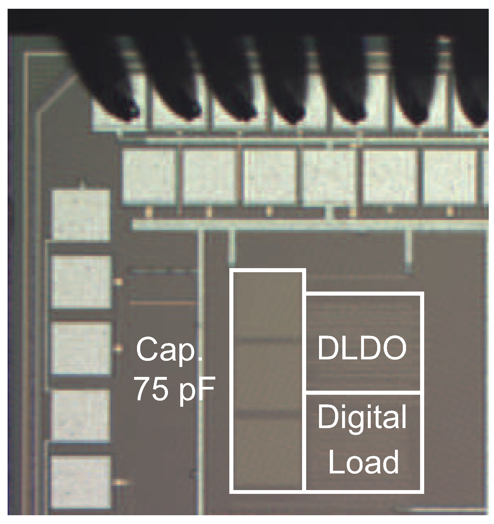
A 9-bit D-LDO was implemented in an active area of 0.035 at a 55-nm general-purpose Global Foundries CMOS process. The implementation also includes a digital controlled current source load and a 75 load capacitance. Figure 6 illustrates the die photo of the implemented design.
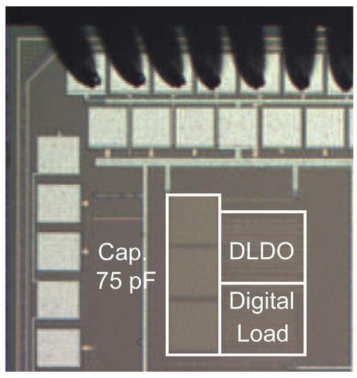
Figure 6.
Die photo of the fabricated D-LDO regulator.
The assessment of the performance of the load regulation in terms of transient performance is performed with the aid of Figure-Of-Merit [15], described in (2), which suits to ultra-low-power applications.
In case that a design is implemented in an incomparable process, FOM scaling is performed to 55 according to (3)
which allows the equal assessment among the designs. The measurements were performed with wafer probes at probe station chamber under constant temperature of 28 C. Figure 7 illustrates the measurement setup. As shown, the reference signals , , are produced externally, while the , , signals power the system, the digital load and feed the regulated output respectively. Meanwhile, D bus controls the digital selection of specific current load.

Figure 7.
Measurements setup.
4. Measurements Results
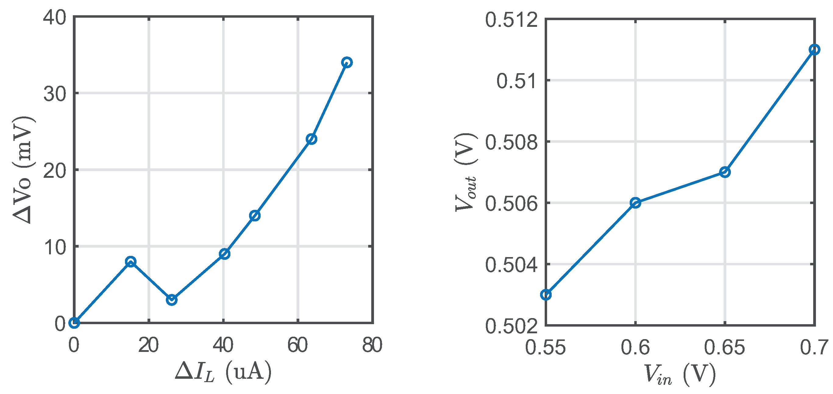
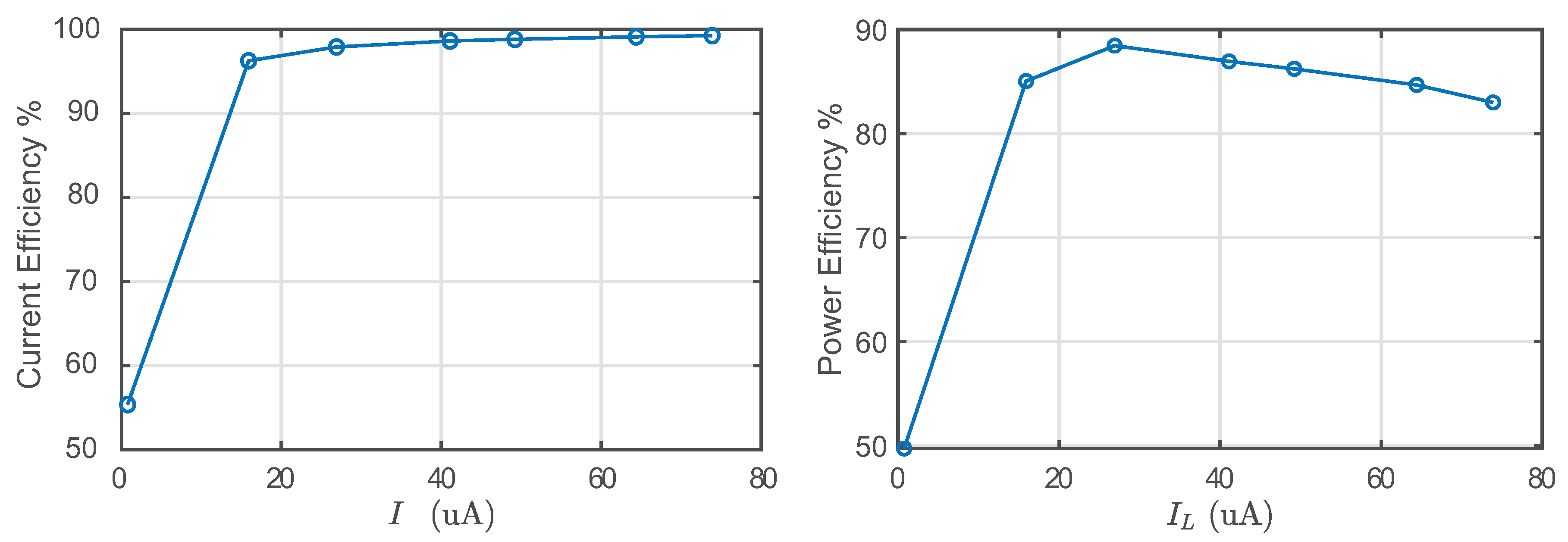
With and , the quiescent current was measured and it varies from 558 to 621 for load current of 764 to 73.9 . To elaborate more, the off-state quiescent current of the oscillator consumes 8% of the total minimum quiescent current, Comp 3 and Comp 4 50%, Comp 1 27% while the remaining 15% is distributed to the voltage divider, power-on-reset circuit, current distribution circuitry, and leakage current of the control circuitry. The reference of output regulation voltage is fixed at 0.5 V during measurements such that maximum power efficiency is achieved for given drop-out voltage and load current. Figure 8 illustrates the steady-state measurements of the current efficiency and voltage regulation. As illustrated, the maximum load regulation comes at 528 / and maximum line regulation of 120 mV/V was observed. As seen at Figure 9, for current load more than 15.9 , the minimum measured efficiency is 96.2% while the maximum value reaches 99.2%. The maximum value of power efficiency is 88.5%, which is higher than 76% as reported for SoC-IoT-oriented analog LDO [4]. Hybrid implementation of the regulator as presented in [12] combines inductor-based switching regulator with D-LDO and naturally shows off higher power efficiency of 94%. However, higher efficiency comes at the expense of higher power consumption of 30.5 total system quiescent current.

Figure 8.
Voltage and load regulation experimental measurements.
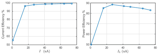
Figure 9.
Power and current efficiency experimental measurements.
Figure 10 illustrates the transient response of the implemented regulator under load surge that alternates between 764 and 73.9 . We measured 156 mV droop with load step 4 from 764 to 73 current load surge. As load step happens, the multi-vibrator ”wakes-up” and ”forces” negative clock edge within 600 ns of total system response. The clock period is 4 while the settling time 20 .
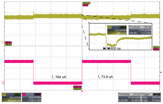
Figure 10.
Transient experimental measurements.
Table 1 shows the performance comparison of the proposed design with prior D-LDO implementations. Architectures that employ adaptive controllers as presented by [9,11,13] are based on adaptive sampling frequency for faster regulation. However, among them, architectures that employ complex digital computational units [9,11] occupy a larger active area of 0.057 and 0.165 respectively. In terms of FOM comparison, dynamic frequency scaling architectures [9,13] lack behind the rest. Moreover, it is observed that the transient test of [15] has been performed with 500 load step that compared to 4 of this work is 125 times slower while the FOM of this work remains 3.5 times bigger than the presented transient test at [15]. Furthermore, the FOM as achieved in [14] is naturally less than the FOM presented in Figure 10 as it uses state-of-the-art self-biased comparators in contrast to conventional comparators of this work.

Table 1.
Comparison with prior-art D-LDOs.
5. Conclusions
A D-LDO that constitutes the main regulator of an ultra-low-power and ultra-low-voltage SoC-IoT application should incorporate an integrated clock generation unit. To fulfill this requirement, we propose a D-LDO design aimed at micro-power IoT systems that is based on a burst oscillator that offers instant response under transient load. In contrast to ring-oscillator-based topologies, the event response of the proposed burst oscillator is not constrained by the system design specification of the operational frequency. The D-LDO regulator as implemented shows off 558 minimum quiescent current and 99.2% maximum current efficiency with a 1.16x improvement of power efficiency compared to analog-LDO oriented to ultra-low-power IoT loads.
Author Contributions
Conceptualization, C.K. and T.U.; writing—original draft preparation, C.K.; writing—review and editing, C.K.; supervision, T.U.; project administration, T.U.; funding acquisition, T.U. All authors have read and agreed to the published version of the manuscript.
Funding
This research received no external funding.
Acknowledgments
The authors wish to acknowledge the support of the Austrian Research Promotion Agency (FFG) within the project ’BaKoSens 4.0’ (Grant No. 8633205).
Conflicts of Interest
The authors declare no conflict of interest.
References
- Yahya, F.B.; Lukas, C.J.; Calhoun, B.H. A Top-Down Approach to Building Battery-Less Self-Powered Systems for the Internet-of-Things. J. Low Power Electron. Appl. 2018, 8, 21. [Google Scholar]
- Chua, A.; Maestro, R.J.; Jardin, J.C.; Monisit, K.; Nuestro, R.; Fabay, K.B.; Pelayo, B.R.; Lofamia, W.V.; Ortiz, J.R.; Madamba, J.A.; et al. Smart-wire: A 0.5 V 44 μW 0 °C to 100 °C power-line energy harvesting sensor node. In Proceedings of the 2017 IEEE Custom Integrated Circuits Conference (CICC), Austin, TX, USA, 30 April–3 May 2017; pp. 1–4. [Google Scholar] [CrossRef]
- Zangi, U.; Feldman, N.; Hadas, T.; Dayag, N.; Shor, J.; Fish, A. 0.45 v and 18 μA/MHz MCU SOC with Advanced Adaptive Dynamic Voltage Control (ADVC). J. Low Power Electron. Appl. 2018, 8, 14. [Google Scholar] [CrossRef]
- Quelen, A.; Badets, F.; Pillonnet, G. A sub-100 nW power supply unit embedding untrimmed timing and voltage references for duty-cycled μW-range load in FDSOI 28 nm. In Proceedings of the ESSCIRC 2017—43rd IEEE European Solid State Circuits Conference, Leuven, Belgium, 11–14 September 2017; pp. 279–282. [Google Scholar]
- Mu, J.; Liu, L.; Zhu, Z.; Yang, Y. A 58-ppm/°C 40-nW BGR at Supply From 0.5 V for Energy Harvesting IoT Devices. IEEE Trans. Circuits Syst. II Express Briefs 2017, 64, 752–756. [Google Scholar] [CrossRef]
- Mu, J.; Liu, L.; Zhu, Z.; Yang, Y. A 0.5 V, 40 nW voltage reference for WBAN devices. In Proceedings of the 2016 IEEE Biomedical Circuits and Systems Conference (BioCAS), Shanghai, China, 17–19 October 2016; pp. 504–507. [Google Scholar] [CrossRef]
- Shrivastava, A.; Craig, K.; Roberts, N.E.; Wentzloff, D.D.; Calhoun, B.H. 5.4 A 32 nW bandgap reference voltage operational from 0.5 V supply for ultra-low power systems. In Proceedings of the 2015 IEEE International Solid-State Circuits Conference—(ISSCC) Digest of Technical Papers, San Francisco, CA, USA, 22–26 February 2015; pp. 1–3. [Google Scholar] [CrossRef]
- Lahiri, A.; Badrathwal, P.; Jain, N.; Chatterjee, K. A 0.5 V supply, 49 nW band-gap reference and crystal oscillator in 40 nm CMOS. In Proceedings of the 2017 IEEE Custom Integrated Circuits Conference (CICC), Austin, TX, USA, 30 April–3 May 2017; pp. 1–4. [Google Scholar] [CrossRef]
- Ahmed, K.Z.; Krishnamurthy, H.K.; Augustine, C.; Liu, X.; Weng, S.; Ravichandran, K.; Tschanz, J.W.; De, V. A Variation-Adaptive Integrated Computational Digital LDO in 22-nm CMOS With Fast Transient Response. IEEE J. Solid State Circuits 2020, 55, 977–987. [Google Scholar] [CrossRef]
- Salem, L.G.; Warchall, J.; Mercier, P.P. A Successive Approximation Recursive Digital Low-Dropout Voltage Regulator with PD Compensation and Sub-LSB Duty Control. IEEE J. Solid State Circuits 2018, 53, 35–49. [Google Scholar] [CrossRef]
- Otsuga, K.; Onouchi, M.; Igarashi, Y.; Ikeya, T.; Morita, S.; Ishibashi, K.; Yanagisawa, K. An on-chip 250 mA 40 nm CMOS digital LDO using dynamic sampling clock frequency scaling with offset-free TDC-based voltage sensor. In Proceedings of the 2012 IEEE International SOC Conference, Niagara Falls, NY, USA, 25–28 September 2012; pp. 11–14. [Google Scholar]
- Lee, Y.H.; Peng, S.Y.; Chiu, C.C.; Wu, A.C.H.; Chen, K.H.; Lin, Y.H.; Wang, S.-W.; Tsai, T.-Y.; Huang, C.-C.; Lee, C.C. A Low Quiescent Current Asynchronous Digital-LDO With PLL-Modulated Fast-DVS Power Management in 40 nm SoC for MIPS Performance Improvement. IEEE J. Solid State Circuits 2013, 48, 1018–1030. [Google Scholar] [CrossRef]
- Nasir, S.B.; Gangopadhyay, S.; Raychowdhury, A. All-digital low-dropout regulator with adaptive control and reduced dynamic stability for digital load circuits. IEEE Trans. Power Electron. 2016, 31, 8293–8302. [Google Scholar] [CrossRef]
- Kim, D.; Kim, S.; Seok, M.; Ham, H.; Kim, J. 0.5 V—Vin, 165-mA/mm2 fully-integrated digital LDO based on event-driven self-triggering control. In Proceedings of the 2018 IEEE Symposium on VLSI Circuits, Madurai, India, 28–30 June 2018; pp. 109–110. [Google Scholar]
- Li, S.; Calhoun, B.H. 14.6 a 745 pA hybrid asynchronous binary-searching and synchronous linear-searching digital ldo with 3.8 105 dynamic load range, 99.99% current efficiency, and 2 mV output voltage ripple. In Proceedings of the 2019 IEEE International Solid- State Circuits Conference—(ISSCC), San Francisco, CA, USA, 17–21 February 2019; pp. 232–234. [Google Scholar]
- Bose, S.; Johnston, M.L. A Stacked-Inverter Ring Oscillator for 50 mV Fully-Integrated Cold-Start of Energy Harvesters. In Proceedings of the 2018 IEEE International Symposium on Circuits and Systems (ISCAS), Florence, Italy, 27–30 May 2018; pp. 1–5. [Google Scholar]
- Saito, T.; Komatsu, S. A low—Voltage hysteresis comparator for low power applications. In Proceedings of the 2017 24th IEEE International Conference on Electronics, Circuits and Systems (ICECS), Batumi, GA, USA, 5–8 December 2017; pp. 427–430. [Google Scholar]
Publisher’s Note: MDPI stays neutral with regard to jurisdictional claims in published maps and institutional affiliations. |
© 2020 by the authors. Licensee MDPI, Basel, Switzerland. This article is an open access article distributed under the terms and conditions of the Creative Commons Attribution (CC BY) license (http://creativecommons.org/licenses/by/4.0/).


