Article

Comparative Modelling and Thermal Analysis of AlGaN/GaN Power Devices

by
Mahesh B. Manandhar
* and
Mohammad A. Matin
Department of Electrical and Computer Engineering, Daniel Felix Ritchie School of Engineering, 2155 East Wesley Avenue, Denver, CO 80208, USA
*
Author to whom correspondence should be addressed.
J. Low Power Electron. Appl. 2021, 11(3), 33; https://doi.org/10.3390/jlpea11030033
Submission received: 30 June 2021 / Revised: 27 August 2021 / Accepted: 30 August 2021 / Published: 3 September 2021

Abstract

:
The use of Aluminum Gallium Nitride (AlGaN) as a power switching device material has been a promising topic of research in recent years. Along with Silicon Carbide (SiC) and Gallium Nitride (GaN), AlGaN is categorized as a Wideband Gap (WBG) material with intrinsic properties best suited for high power switching applications. This paper simulates and compares the thermal and electrical performance of AlGaN and Silicon (Si) MOSFETs, modeled in COMSOL Multiphysics. Comparisons between similar AlGaN/GaN and Si power modules are made in terms of heatsink requirements. The temperatures for the same operating voltage are found to be significantly lower for the AlGaN MOSFETs structures, compared to Si. The heatsink size for the AlGaN/GaN is found to be smaller compared to Si for the power modules.

1. Introduction

Power electronics is an important link between the generation and consumption of electrical energy with multiple transformation stages taking place through power electronic devices. Silicon (Si) has been the main semiconductor basis for power electronic converters, but Si-based electronic technology has matured. A newer generation of power device semiconductor technology is better at fulfilling the need for higher thermal and voltage requirements than Si [1,2,3]. The limited material properties of Si have fueled the development of power semiconductor devices with the superior properties of Wide Bandgap (WBG) materials [1,4]. WBG semiconductor devices have emerged as the simpler and cheaper option compared to using complex techniques to stretch the capabilities of Si [1,3,4,5,6]. The biggest limiting factors impeding Si for higher power device usage are due to its lower blocking voltage, thermal conductivity, and switching frequencies [2,4,5]. WBG materials have properties like higher electrical breakdown voltages and bandgap energies compared to Si, which lead to lower ON resistances. These properties also allow for higher operating voltages and temperatures with lower power losses [4,5]. Silicon Carbide (SiC) and Gallium Nitride (GaN) are two examples of such WBG semiconductors that have more developed markets with commercially available fabrication methods and end products [2]. Different power devices ranging from diodes, Bipolar Junction Transistors (BJTs), Metal Oxide Field Effect Transistors (MOSFETs), Junction Field Effect Transistors (JFETs), Metal Semiconductor Field Effect Transistors (MESFETs), and High Electron Mobility Transistors (HEMT) have been manufactured with these WBG materials [1,7].
Ultrawide-bandgap (UWBG) semiconductors are WBG semiconductors with bandgap energies significantly higher than 3.4 eV of GaN, and are emerging as the next exciting field in semiconductor device research [8,9]. UWBG semiconductor materials include Aluminum Gallium Nitride, Aluminum Nitride (AlN), Diamond, and Gallium Oxide (Ga2O3), and have shown promising advantages in the fields of RF electronics and deep-UV optoelectronics, as well as power electronics [8,9]. AlGaN alloys have exceptionally good electrical properties including a wide range of direct bandgaps from 3.4 to 6.0 eV (depending on Al content), high breakdown fields, and high electron mobilities [8]. AlGaN shares the same crystal structure and material compatibility as Indium Gallium Nitride (InGaN), which is the second most widely used semiconductor material [10], and so can take advantage of the knowledge and manufacturing infrastructure associated with InGaN [8]. GaN power devices have been commercially available since the early 2000s and the development of AlGaN/GaN power devices is an attractive topic of research [11,12,13,14].
Power MOSFETs require a low gate current to operate, with very high input impedance and fast switching capabilities [15,16,17]. Lateral Double-Diffused MOSFETs (LDMOSFETs) and Vertical Double-diffused MOSFET (VDMOSFETs) are two of the most widely used MOSFET structures that employ double-diffusion doping techniques to achieve high precision in channel length [18,19]. The location of the Drain contact relative to the Source terminal differentiates VDMOSFETs from LDMOSFETs, i.e., VDMOSFETs have the Drain vertically below the Source at the bottom of the device substrate, while LDMOSFETs have the Drain laterally across the channel from the Source [18]. Having the Drain terminal below the Source in VDMOSFETs has the advantage of increasing the Source area which helps in reducing the current density and overall device temperatures compared to LDMOSFETs [18]. VDMOSFETs also have a bigger separation between the Drain and Source terminals compared to LDMOSFETs, which increases the operational voltages of the device without breaking down electrically [16,20].
In renewable energy systems like Photovoltaic (PV) inverters, a transformer usually provides galvanic isolation while transforming the output voltage from the input voltage [21,22]. The transformers, however, add to the weight/size and cost of the inverter and also reduce the efficiency and power density due to copper/ iron core losses [21]. Transformerless inverter topologies reduce electric component requirements and overall weight while increasing the system reliability and efficiency of the power conversion system, due to the absence of the additional transformer coils [21,22,23,24]. However, transformerless inverters do have the issue of ground fault currents and leakage currents due to the presence of a parasitic capacitor between the input DC source and ground [21,22]. Various transformerless inverter topologies like the H4, H5, and H6 topologies have been proposed/implemented recently to eliminate the leakage current through techniques such as clamping the common mode (CM) voltage (CMV) during the freewheeling period, or changing the switching times of different power switching devices [21,22,25,26,27,28]. Although H5 and H6 topologies suffer from high conduction losses due to multiple switches conducting current during the active state, such conduction losses can be reduced by forming new current paths and reducing the number of conducting switches during the active state by modifying the switching sequences.
This paper compares the electrical and thermal performance of AlGaN as a material for a VDMOSFET structure with that of Si using COMSOL Multiphysics for the same operating voltage conditions. This paper does not consider the fabrication difficulties of AlGaN VDMOSFETs, but compares the temperatures of a Si VDMOSET with that of an AlGaN one for the same operating voltages. The paper is organized in the following way. A 2D VDMOSFET structure is modeled in COMSOL with Si and AlGaN as the semiconductor material at the same operating voltages of normal operation, and then for breakdown. The thermal performance of the VDMOSFET structures at the same operating voltages are compared, instead of the same power dissipation, to demonstrate AlGaN’s advantage in terms of higher operating voltages. A commercially available AlGaN/GaN HEMT module on a modified H5 transformerless inverter topology is then compared with a similarly rated Si MOSFET module, in terms of heatsink requirements, for the same operating conditions in 3D simulations in COMSOL.

2. Thermal Simulation

2.1. 2D Model of VDMOSFETs with Si and AlGaN

The use of simulation software for modelling thermal performance of power devices has been reported in literature [29,30,31,32,33,34]. Commercial software like COMSOL Multiphysics, Agilent ADS®, ANSYS, etc., are software that use numerical methods, Finite Element, and Finite Volume Methods (FEM and FEV), along with Computer Aided Design (CAD) tools, to model the thermal performance of power devices like HEMTs and MOSFETs in 2D and 3D environments [29,30,31,32]. Software like COMSOL, FLUENT, ANSYS, and Pro-MECHANICA have also been reported in literature for modelling thermal performance of heatsinks [35,36,37,38,39].
For this paper, COMSOL was used to initially study the change in temperatures of the VDMOSFET structures, with Si and AlGaN as semiconductor materials, due to the Joule heating caused by electrical currents flowing through the semiconductor materials of Si and AlGaN under normal MOSFET operating conditions, and then for electrical breakdown conditions. The 2D model of the VDMOSFET structure built in COMSOL in [33] was used with Semiconductor and Heat Transfer physics modules for both these conditions. The steady state effects of different Gate and Drain terminal voltages on the current density and temperature of the structures were studied by creating a stationary study in COMSOL for both models. The electric potential, the electron and hole concentrations, and the temperature within the structure of the VDMOSFET were calculated with the two physics modules in COMSOL [40]. The Semiconductor physics module initially calculated the currents in the structure, and then the Joule heating was produced by the currents with the initial temperature of the VDMOSFET set to a room temperature of 20 °C. The temperature within the device structure was then calculated by the Heat Transfer physics module, using the heat calculated by the Semiconductor module. It was concluded in [33] that the maximum and average temperatures for a 2D VDMOSFET model made with Si was close to two times greater than the maximum temperatures for the same model with GaN for all operating voltages in normal operation.

2.1.1. Model Geometry

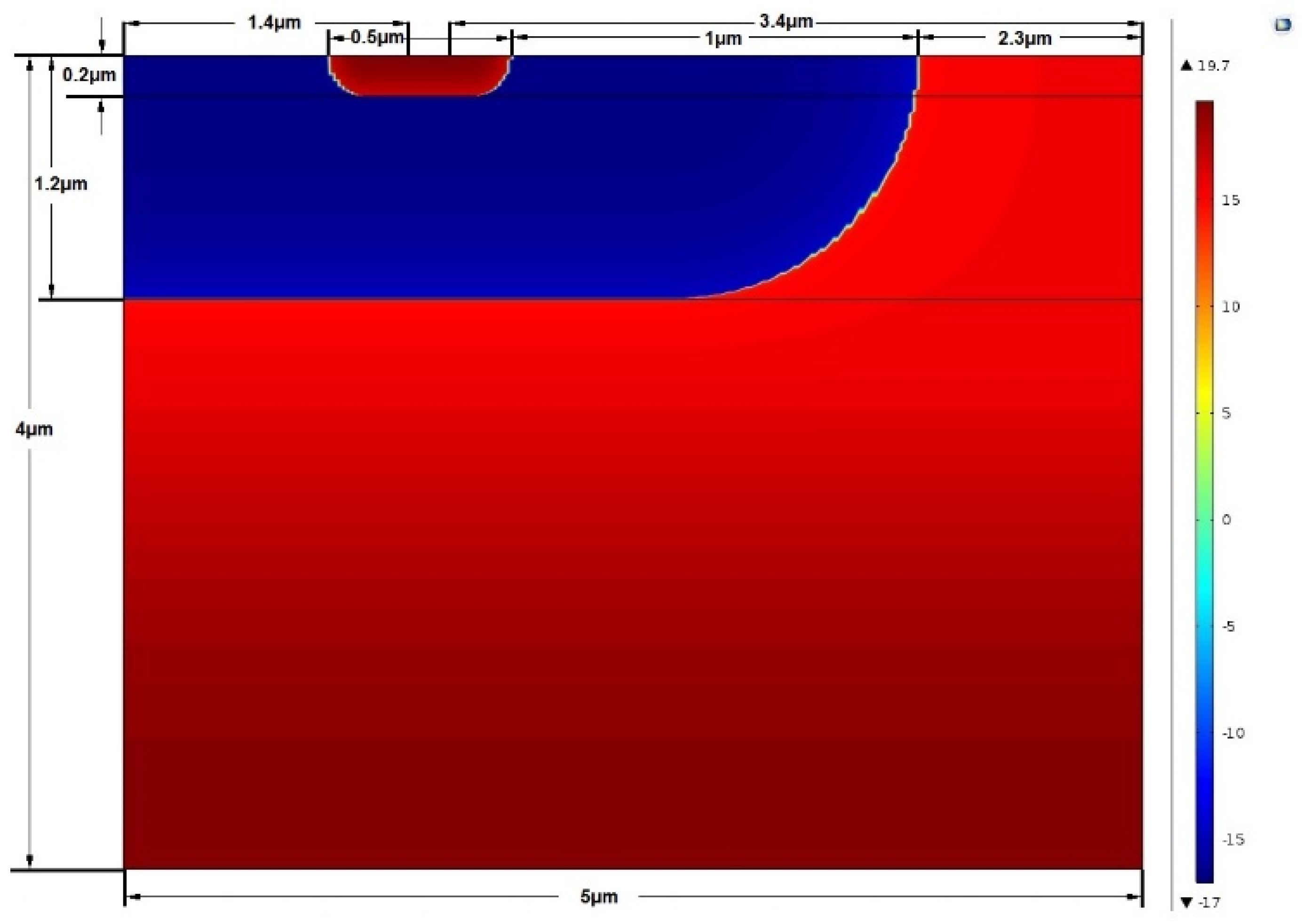
The VDMOSFET structure consists of the Source and Gate terminals on the top, and Drain terminal at the bottom of the device model as seen in Figure 1 [18]. A thin oxide layer insulates the Gate metal contact from the semiconductor material. The Source contact lies on top of a heavily doped p+ region, with a heavily doped n+ region bridging the Source and Gate terminals. A heavily doped n+ region sits on top of the Drain contact. The direct flow of electrons from the Source to the Drain, due to the application of a Drain to Source voltage (VDS) through the n-drift region, is prevented by the heavily doped p- region. A channel is created within this p+ region, and the current can flow from the Source to the Drain when a positive Gate to Source voltage (VGS) is applied. Figure 2 shows a half-cross section of the VDMOSFET with a log of the dopant concentrations from [33], which was used for this paper. N-type dopants are represented by Red, and p-type dopants are represented by Blue in Figure 2. The dimensions and geometry of the VDMOSFET structure were obtained from [20]. The model meshing for both VDMOSFET structures consisted of 4680 quad elements with a meshing area of 20 μm2.

2.1.2. Boundary Conditions

The materials used were considered isotropic, with all material properties uniform in all directions. A total of six boundary conditions were set for the Semiconductor physics, while three boundary conditions were set for the Heat Transfer in Solid physics. The vertical left edge in Figure 2 was set to have Axial symmetry for both physics involved. The Source and Drain terminals were set as Metal Contact boundary conditions, and a Thin Insulator Gate boundary condition with an insulator thickness of 0.1 μm was set for the Gate [33]. All three terminals had Convective Heat Flux boundary conditions to simulate convective heat losses from the terminal contacts to the ambient air without any forced cooling. Continuity boundary conditions were set for the two inner boundaries between the top and bottom surfaces to represent semiconductor material continuity without any heterojunction due to different materials within the VDMOSFET structure, and the remaining boundaries were set as thermal and electrical insulators.

2.1.3. Material Properties

The material properties for Si and AlGaN were used from predefined material libraries in COMSOL. Table 1 shows the material properties for the semiconductor materials. The effective density of states in the conduction and valence band are temperature dependent, and are expressed in terms of the absolute temperature in K in Table 1. The material properties of AlGaN depend upon the mole fraction of Al present in the AlGaN alloy represented by x as AlxGa1−xN. A greater value of x makes the material properties closer to AlN, and the smaller value of x makes the properties closer to GaN. Most of the properties for the AlGaN available on COMSOL were for Al0.15Ga0.85N, with 15% Aluminum and 85% Gallium for the Group III elements in the alloy and, hence, the physical properties are closer to GaN for this Al0.15Ga0.85N alloy. The thermal conductivity for AlGaN was obtained from [41].

2.1.4. Semiconductor Physics Modeling

The semiconductor physics module in COMSOL uses partial differential equations with the conventional drift-diffusion approach to solve for the dependent variables of electric potential, and electron and hole concentrations [40]. The module solves Poisson’s equation and current continuity equations, to solve for the values of these dependent variables [40].
Dopant concentrations usually vary with a Gaussian decay profile when going away from the external surfaces of the semiconductor substrate where the dopants are deposited, so Gaussian decay profiles were used for the doping models for all doped regions [33]. The heavily n+ doped region and heavily p+ doped region had maximum dopant concentration values of 5 × 1019 cm−3 and 1 × 1017 cm−3, respectively, while the n- drift region had a maximum dopant concentration value of 5 × 1015 cm−3 for normal operating conditions, as obtained from [20]. To simulate electrical breakdown conditions, these dopant concentrations were scaled down by a factor of 100 instead of increasing the terminal voltages.

2.1.5. Heat Transfer Physics Modeling

The semiconductor module calculates the heat generated in the semiconductor structure by Joule heating and charge carrier generation-recombination processes, and these were set as the heat source for the Heat Transfer in the Solids physics module to solve for the temperatures of the devices. The metal terminals of the VDMOSFET were set to be exposed to ambient air at room temperature of 20 °C, and appropriate convective heat flux boundary conditions without any forced air movements were set to simulate this loss of heat.

2.1.6. Model Simulation and Results

The input variables for both normal operation and breakdown models were the VDS and VGS values, with the Source terminal remaining at ground potential. Parametric sweeps for VGS and VDS were configured to go from 0 V to 20 V for VGS and from 0 V to 55 V for VDS for the normal operation model of Si. VGS was swept from 0 V to 20 V and VDS from 0 V to 49 V for the AlGaN model for the same mode of operation. The same sweeps of 0 V to 20 V were made for VGS for both Si and AlGaN model in breakdown mode while VDS was swept from 0 V to 40 V for the same. The study steps of the model were set such that the solutions from one combination of input voltages were reused as initial solutions for the next combination of voltages. The values for VGS and VDS were not ramped up in equal voltage intervals, as certain voltage values gave incomplete solutions. Appropriate meshing of the geometries was set for optimal convergence of solutions in all the models.
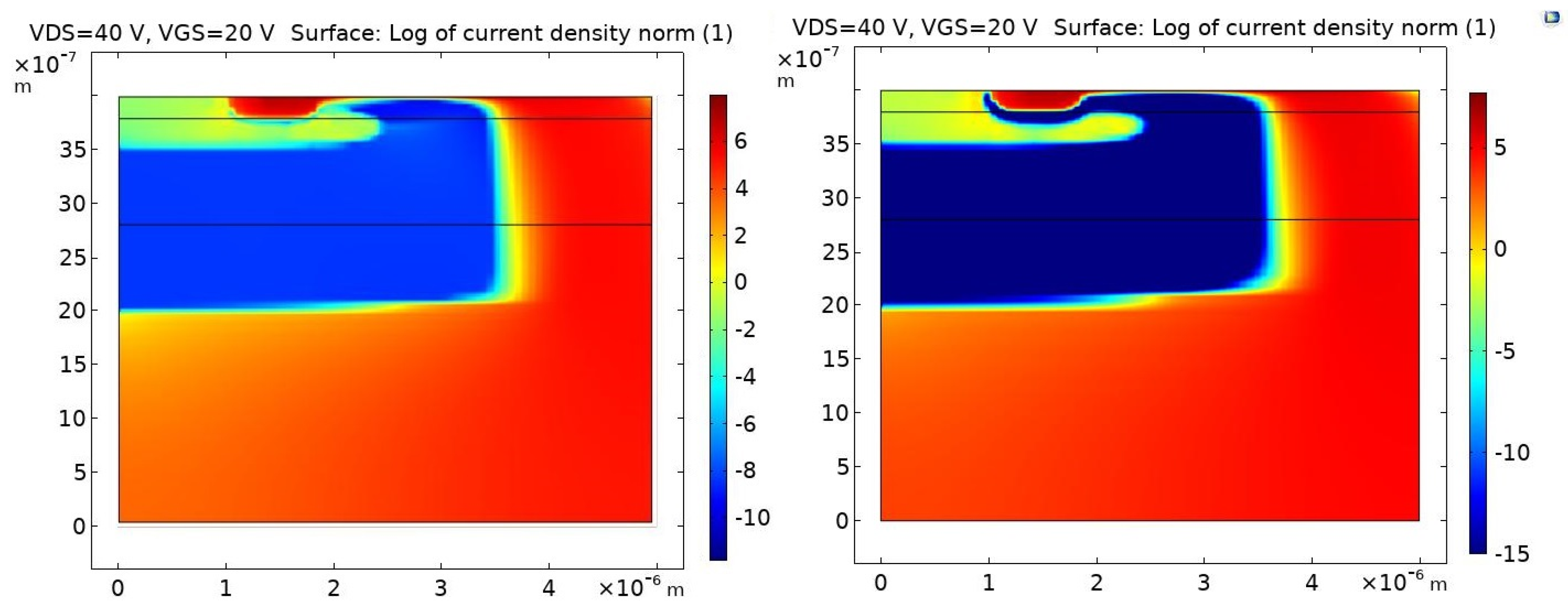
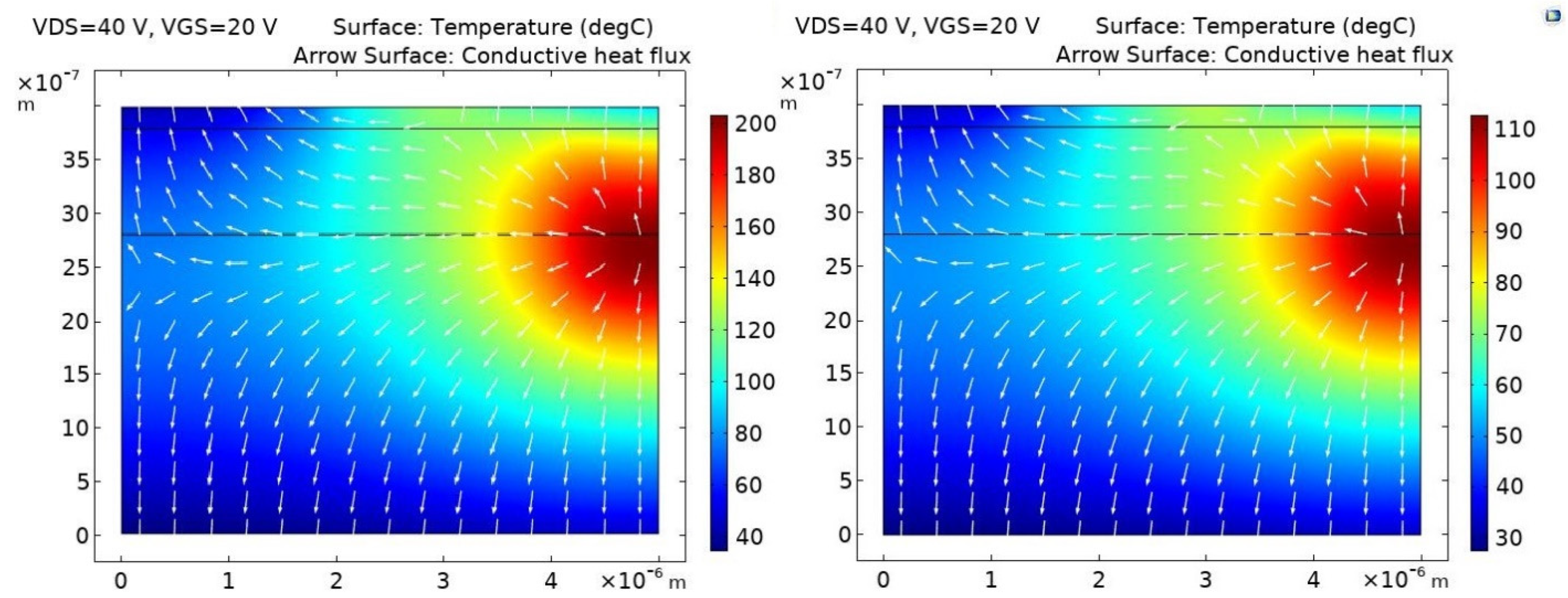
Figure 3 compares the log of norm of the current density components for the Si and AlGaN VDMOSFETs under normal operating conditions of VDS = 40 V and VGS = 20 V, and it shows the highest current densities occur just below the Gate terminal. The current is seen flowing from the Source on the left to the Drain on the bottom through the narrow conducting channel created from left to right. The heavily doped p- region in the blue prevents the direct flow of current vertically from the Source to the Drain under normal operating conditions. Figure 4 shows the distribution of temperatures for the Si and AlGaN structures for the same operating conditions with the highest temperatures occurring at the location as the high current densities for both models. The arrows in the figure show the direction of heat flux going away from areas of higher temperatures to areas of lower temperatures. This figure also shows the maximum temperatures for this combination of VGS and VDS is almost twice as high for the Si device when compared to the AlGaN device.
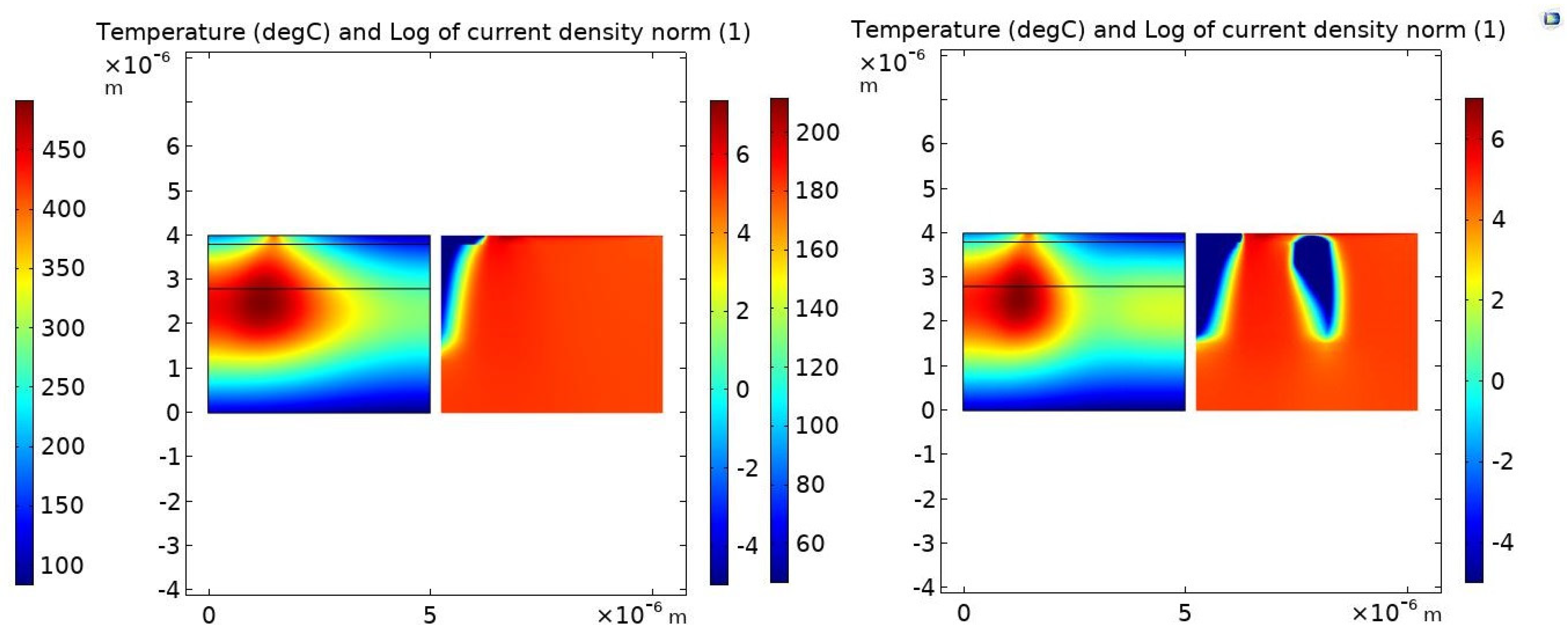
Figure 5 shows the temperature and log of norm of current density profiles for the Si and AlGaN VDMOSFETs for the lower dopant concentration levels for the same operating voltages of VDS = 40 V and VGS = 20 V. The low p- region dopant concentrations mean that even low Drain voltages can allow for electrons to punch through the p regions directly and cause the current to flow vertically from the Drain to the Source. There is no narrow channel required for this current flow compared to Figure 3, and the current densities are almost three times higher when compared to the higher dopant concentration level simulations of Figure 3. The temperatures are also more than double when compared to Figure 4, with higher temperatures occurring at regions with higher current densities.
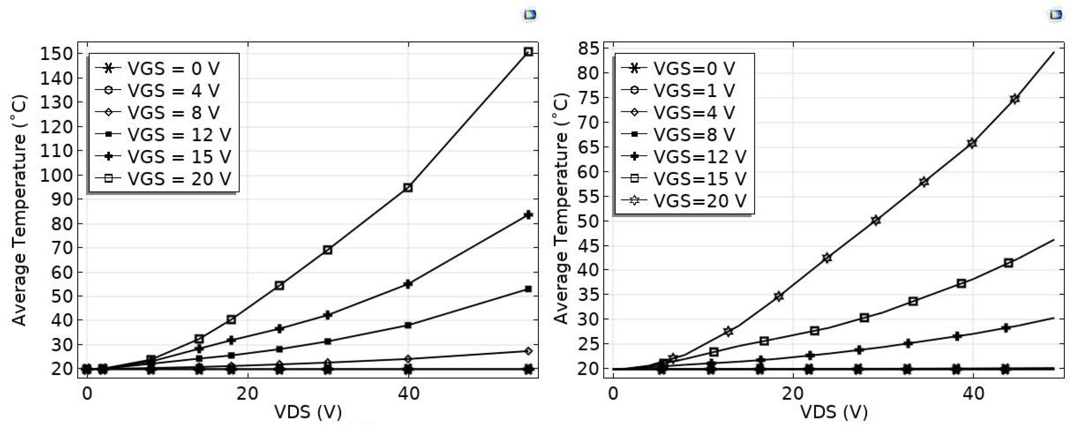
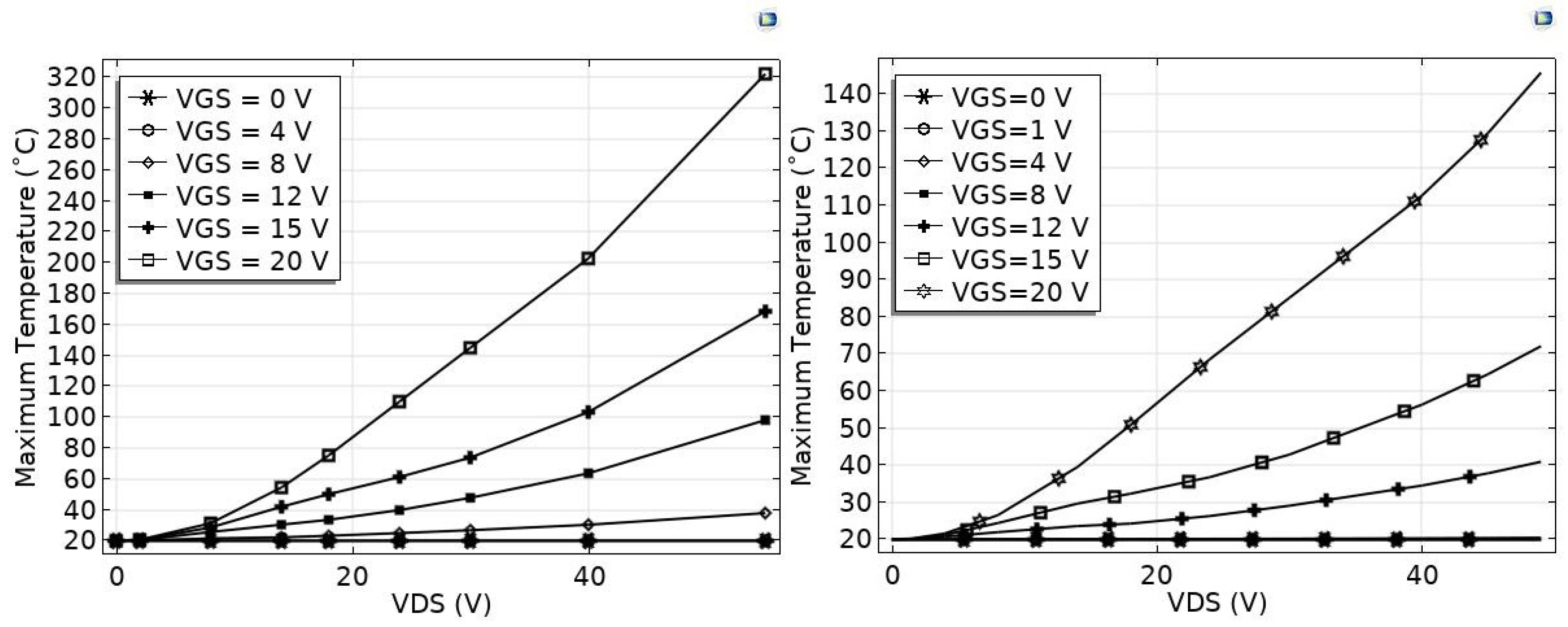
Figure 6 shows the average temperatures for the Si and AlGaN models for normal operation conditions, and Figure 7 shows the maximum temperatures for the two models for the breakdown conditions. The maximum and average temperatures are greater for Si compared to AlGaN for all operating voltages. For small VGS values, the current flow is minimal for both devices, as a channel is not created for low voltages and, so, the temperatures are also close to room temperature. As VGS and VDS are increased, greater current starts to flow through the channel, and the temperatures rise as well. For the same operating voltages values, the maximum temperatures range from about 7% to 45% higher for Silicon compared to AlGaN, and the average temperatures have a similar trend ranging from 2% to 30% higher for Silicon. The maximum temperatures in Si models were over 3.5 times higher compared to SiC, and about twice that of GaN, while the average temperatures were almost three times more in Si compared to SiC, and almost twice compared to GaN, as reported in [33]. Comparing the results of [33] for the same operating conditions and device structure, SiC had the lowest maximum and average temperature, followed by AlGaN and GaN. As an example, the maximum temperature for Si exceeded 280 °C for a VDS of 50 V and VGS of 20 V, while for the same conditions, SiC, GaN, and AlGaN had maximum temperatures of less than 90 °C, 180 °C, and 145 °C, respectively. The difference in average and maximum temperatures between Si and AlGaN start to become significantly large once the VDS is at 18 V and VGS is at 12 V. For most terminal voltages below these values, the average and maximum temperature differences between Si and AlGaN are below 5 °C and 10 °C, respectively, due to the fact that the channel is not created for low VGS values which results in low currents and, hence, lower temperatures.
For the same VGS and VDS values, the power dissipated on the AlGaN device were about 0.5 times less compared to the Si device. For instances of same power dissipation at the same VGS values, the temperatures were between 5 to 12 °C less for the AlGaN device compared to the Si device. For the same power dissipated, the temperature difference is not twice as small compared with the same VGS values, but the temperatures are found to be lower for the AlGaN device. The temperatures are lower for both the same power dissipation and same operating voltages, but the temperatures are much lower for the same operating voltages than for the same dissipated power. The power dissipation for the two devices is shown in Figure 8.
For the breakdown conditions of low dopant concentrations, the current and temperatures ramp up much faster when compared with the normal operating conditions of high dopant concentrations. Conduction of the current begins even at 0 V gate voltage, and so the temperatures start rapidly going up for both Si and AlGaN models. Figure 9 clearly shows that the maximum temperatures in the Si model for the breakdown conditions are over twice the temperatures for the AlGaN model for the same VGS and VDS values, with temperatures going over 450 °C for the highest voltage combination in the Si model, and over 210 °C for the same in the AlGaN model.

2.2. 3D Thermal Modeling of Multipack Switching Devices

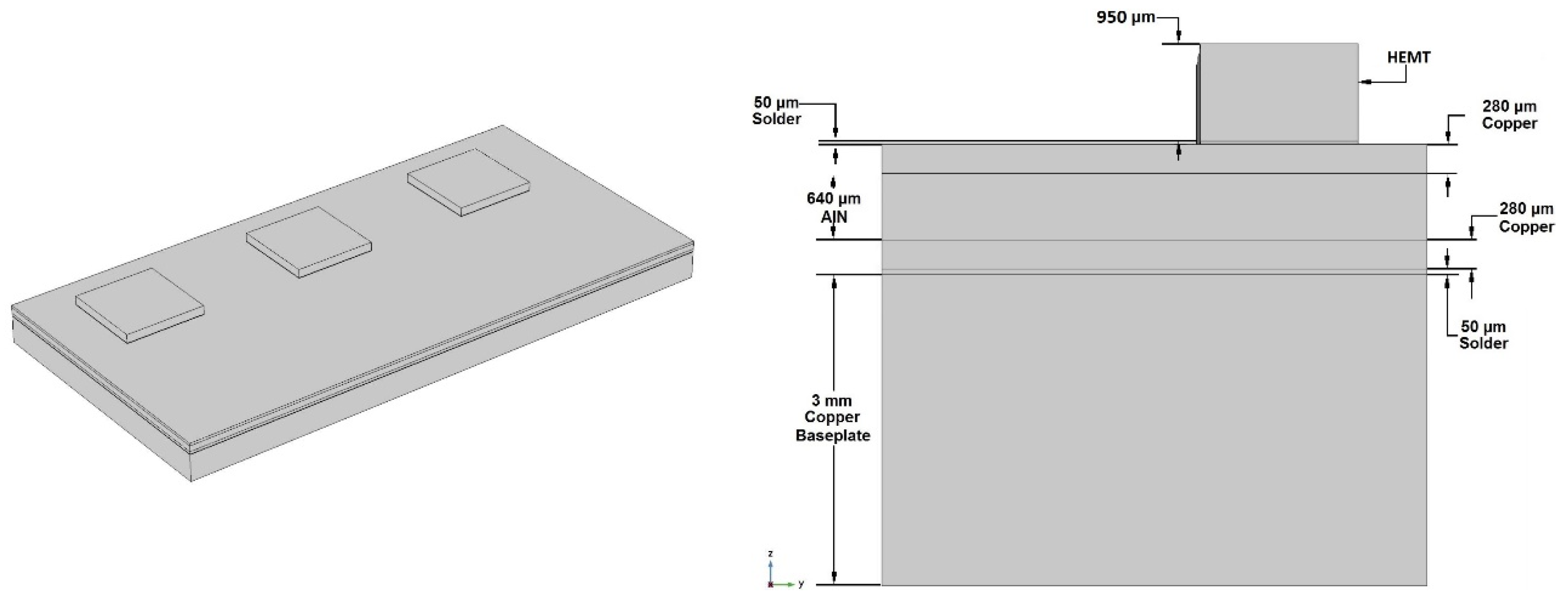
Transformerless power inverters use devices like MOSFETs and HEMTs as their switches, and manufacturers produce these switches in units with multiple switches in a single semiconductor package. In [24], a six-pack module with six GaN HEMTs were modeled in COMSOL to compare the GaN module with a Si module of comparable specifications. Heatsinks were added to these modules to reduce the structures’ temperatures and to compare each material’s thermal performance. AAVID Genie, an online tool from heatsink manufacturer Boyd Corp, was used to compare and verify the results of the COMSOL simulations with their commercially available heatsinks [24]. This module, shown in Figure 10, was used as the basis for generating a HEMT module using three of the commercially available 2-in-1 AlGaN/GaN HEMT units of similar power rating, manufactured by STMicroelectronics. Instead of creating a semiconductor model to obtain temperature values for the entire module, the Joule heating generated by electric currents passing through each of the MOSFET/ HEMT switches were obtained from calculations made in PSIM, which acted as the heat sources for each switch in COMSOL. Figure 11 shows the modified H5 tranformerless topology simulated in PSIM, used to obtain power losses for each HEMT switch. The simulations were conducted with operating conditions of System Power 5 kW, Input DC Voltage 400 V, Output AC Grid Voltage 120 V, Grid Frequency 60 Hz, Switching Frequency 50 kHz, and unity power factor [24].
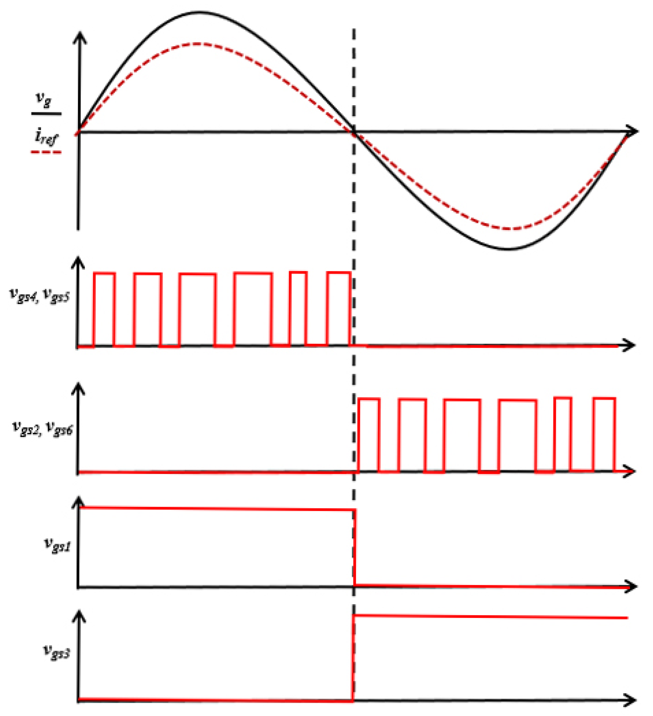
Figure 12 shows the PWM switching sequence for each of the switching devices (S1–S6) in the inverter circuit of Figure 11 [24]. The circuit was simulated with resistive load with a power factor of 1 and, hence, the load voltage and current are in phase. The PWM signals also show that a maximum of three switches conduct current during the active state and one switch and one diode conduct during the zero state. In the positive half cycle, S1, S5, and S4 are turned ON in the active state, and S1 and D3 conduct in the zero state. For the negative half cycle, S2, S6, and S3 conduct in the active state, and S3 and D2 conduct in the zero state S3 and D2. The LCL filter in Figure 11 smoothens out the output to a sinusoid for the output voltage and current.
The physical dimensions of the six-pack module were obtained from [42]. The dimensions of the heatsink for the AlGaN model were made smaller than the one for Si to illustrate the advantages of AlGaN over Si and to compare the heatsink requirements for similar steady state temperatures. The effects of thermal stresses and physical deformation were not simulated for the purposes of this paper.

2.2.1. Model Geometry

The six-pack Si HEMT module in Figure 10 consisted of six TK35A65W5 MOSFETs manufactured by Toshiba mounted on a six-pack MOSFET module of similar power specifications obtained from [42]. The Si MOSFETs and diodes of this module were replaced with the GaN HEMTs, while keeping the multiple layers of other materials the same [24]. The dimensions and different layers along with the Si MOSFETs and Si diodes are shown in Figure 10. Figure 13 shows the MASTERGAN1 AlGaN/GaN HEMTs manufactured by STMicroelectronics replacing the Si MOSFETs and diodes in the six-pack HEMT module. Each MASTERGAN1 HEMT package consists of two HEMTs and, hence, only three of these HEMT packages are placed on the module in COMSOL. The TK35A65W5 is rated at 650 V with RDSON of 80 mΩ, while the MASTERGAN1 is rated at 650 V with RDSON of 150 mΩ [43,44]. The dimensions of the MASTERGAN1 were obtained from [44].
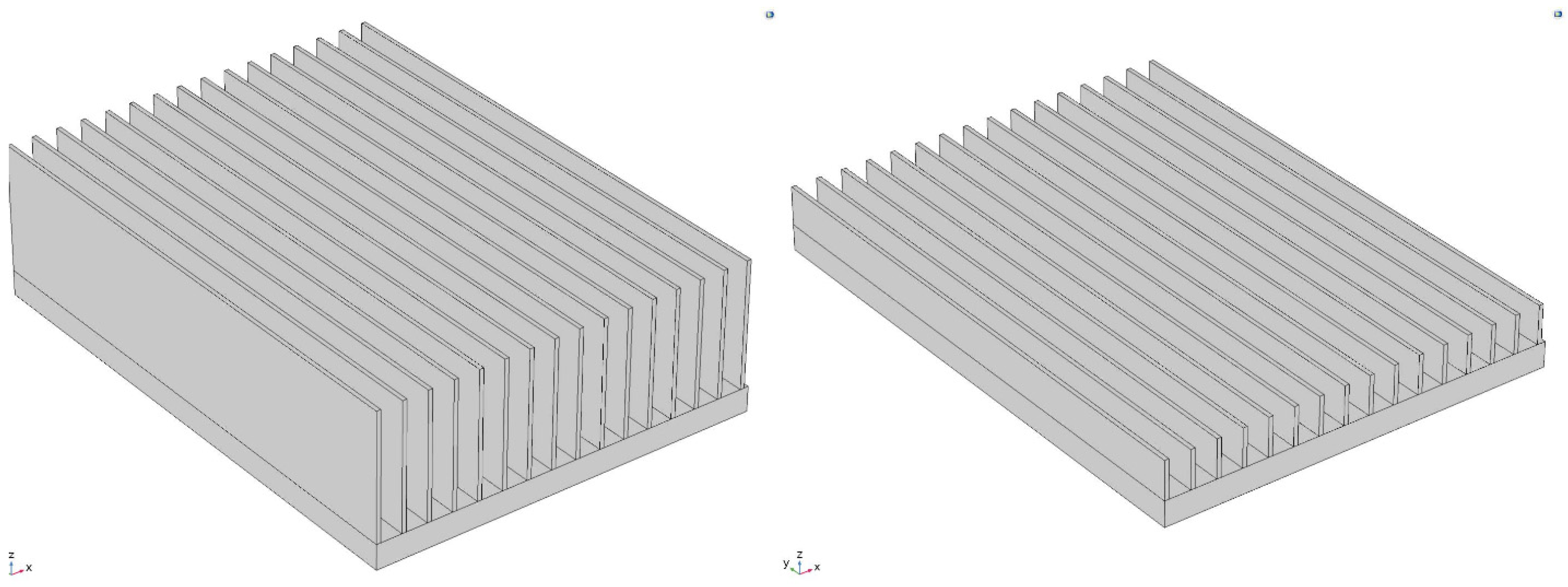
Both models had an Aluminum heatsink placed on the top of the switching devices for cooling. The dimensions of both heatsinks were based on actual heatsinks sold by Boyd Corp. The dimensions were chosen such that the maximum temperatures of the module-heatsink combinations were kept below 100 °C without any forced convective air-cooling mechanisms. Figure 14 shows the heatsinks used for the Si and AlGaN/GaN modules, respectively. Each heatsink was made up of a solid Aluminum block of dimensions 141.8 mm × 104.3 mm × 6.6 mm, with 16 additional aluminum fins of width 1.134 mm separated by 6.8 mm. The height of the fins was set to 33.5 mm and 10 mm for the Si and AlGaN/GaN models, respectively.

2.2.2. Material Properties

The material properties required for calculating the temperatures for the models were Density (ρ), Heat capacity at constant pressure (Cp), and Thermal conductivity (k). The materials were assumed to be isotropic. All the material properties used were built into the COMSOL library, except for the SAC396 solder. The properties of the SAC396 solder were obtained from [45]. Table 2 shows these three material properties for all the materials modeled.

2.2.3. Heat Transfer Physics Modelling

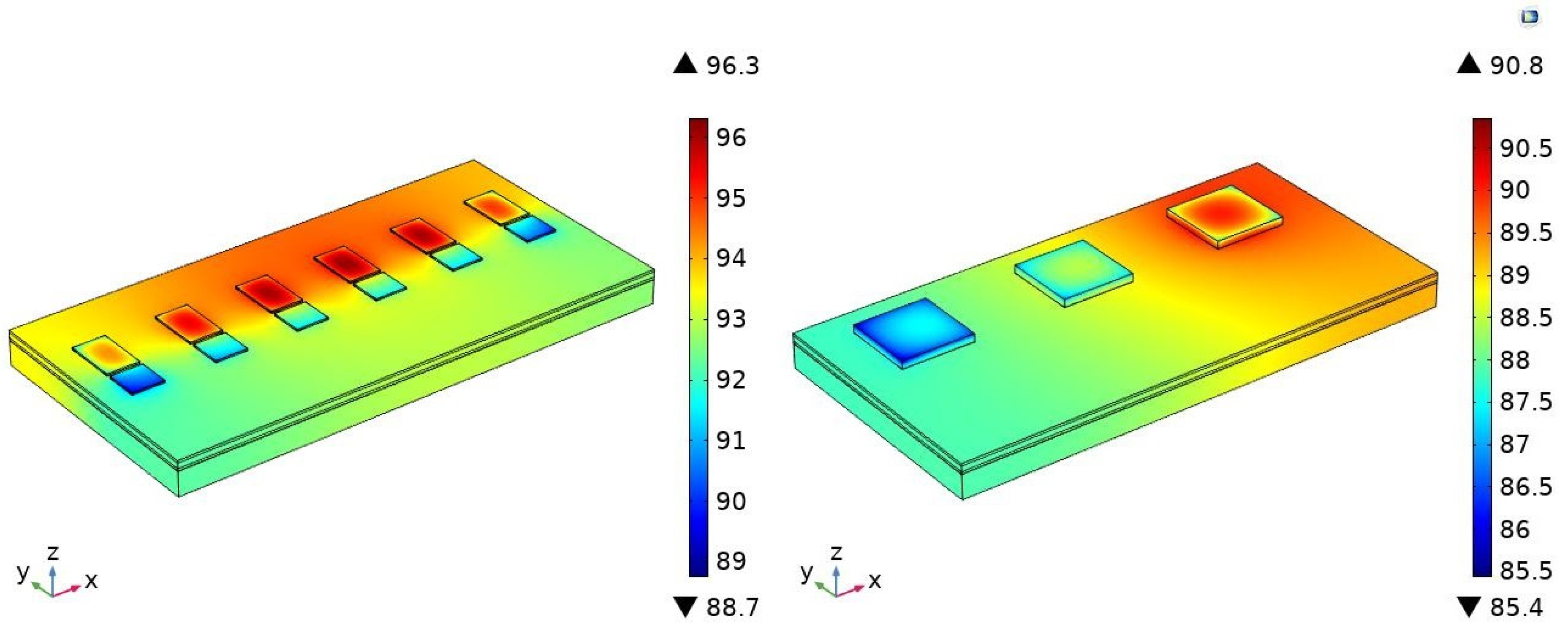
The heat transfer in the Solids physics module of COMSOL was used to calculate the temperatures of the two models. The power losses calculated from PSIM for each semiconductor device module were used as the heat sources for the COMSOL simulations. The power losses for the six Si MOSFETs were calculated in PSIM to be 19.9 W, 19.9 W, 19.9 W, 19.9 W, 21.3 W, and 21.3 W from left to right in Figure 10. The power losses for the three AlGaN/GaN HEMTs in Figure 13 were set to 14.2 W, 14.2 W, and 25.6 W from left to right. A convective heat flux boundary condition for all heatsink surfaces in contact with air was set to simulate the cooling effect of the heatsink with ambient air. A convective heat transfer coefficient of 10.45 W/m2·K was set, which is the heat transfer coefficient for free moving air.

2.2.4. Model Simulation and Results

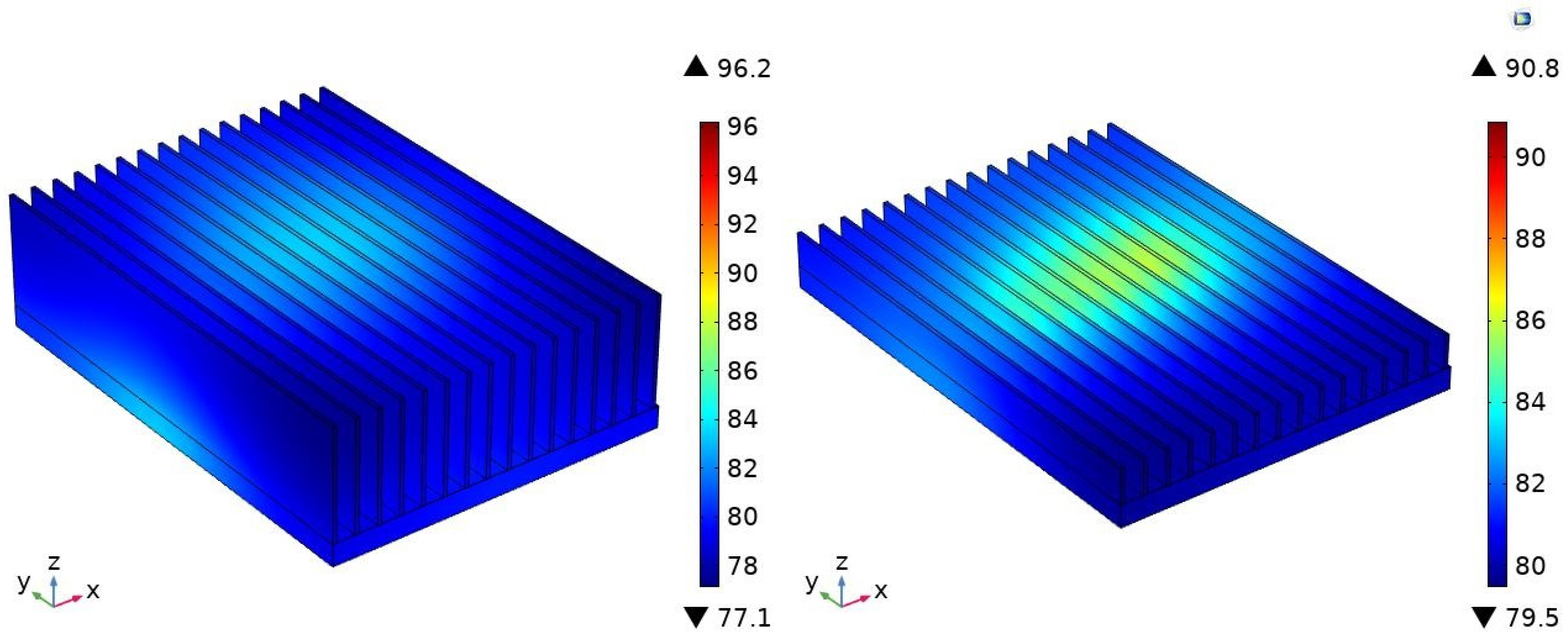
Figure 15 shows the temperature profiles of the GaN and AlGaN/GaN models with the heatsinks hidden. Figure 16 shows the temperature profiles for the Si and AlGaN/GaN models with the heatsinks visible. The temperatures displayed on the legends are in °C.
The maximum temperatures for the Si and AlGaN/GaN models were found to be 96.36 °C and 90.91 °C, respectively. The minimum temperatures were 77.14 °C and 79.47 °C for the Si and AlGaN models, respectively. The Si model had a heatsink volume of 183.8 cm3 and surface area of 1860.5 cm2, while the AlGaN/GaN model’s heatsink had a volume of 123.34 cm3 with a surface area of 785.67 cm2. The maximum temperature, minimum temperature, and heatsink volume for the model in [24] for the GaN Systems GS66516T GaN HEMT were 85.91 °C, 76.87 °C, and 125.6 cm3, respectively.
The temperature profiles of the switching modules for both Si and AlGaN/GaN devices show that the highest temperatures occur at the devices with the highest power losses. The AlGaN/GaN model is within 5 °C compared to Si in terms of maximum and minimum temperatures, with a total heatsink volume about 1.5 times smaller than that for Si.

3. Conclusions

The VDMOSFET models clearly show the thermal superiority of AlGaN as a semiconductor material under normal operations compared to Si for VDMOSFET structures, with temperatures being close to 50% higher for Si than for AlGaN. These results are similar to WBG VDMOSFETs simulated in [33], with AlGaN performing similarly to GaN in terms of temperatures in normal modes of operation. The AlGaN structure was also found to have lower temperatures for the same power dissipation, although not as significantly as for the same operating voltages. For the electrical breakdown conditions, AlGaN performs twice as well in terms of keeping the temperatures low. These simulations do not consider the application of heatsinks in reducing the temperatures. These results demonstrate the thermal advantage of AlGaN for MOSFET structures operating at high voltages. The simulations for the multipack switching devices compare the use of heatsink for Si and AlGaN/GaN switching modules and show that the AlGaN/GaN module requires a heatsink about 1.5 times smaller when compared to the Si module for similar temperatures. These results are also close to the ones for GaN HEMT switches in [24], which required a heatsink of about 1.46 times smaller than that for the same Si module, as simulated in this paper. In conclusion, this paper demonstrates the thermal advantage of AlGaN as a semiconductor material for power switching devices.

Author Contributions

Conceptualization, M.B.M.; data curation, M.B.M.; methodology, M.B.M.; project administration, M.B.M. and M.A.M.; supervision, M.A.M.; validation, M.A.M.; writing—original draft, M.B.M.; writing—review & editing, M.A.M. All authors have read and agreed to the published version of the manuscript.

Funding

This research received no external funding.

Data Availability Statement

Data sharing not applicable.

Conflicts of Interest

The authors declare no conflict of interest.

References

  1. Millán, J.; Godignon, P. Wide Band Gap power semiconductor devices. In 2013 Spanish Conference on Electron Devices; IEEE: Valladolid, Spain, 2013. [Google Scholar]
  2. Millan, J. A review of WBG power semiconductor devices. In Proceedings of the CAS 2012 (International Semiconductor Conference), Sinaia, Romania, 15–17 October 2012. [Google Scholar]
  3. Ozpineci, B.; Tolbert, L.M.; Islam, S.K.; Chinthavali, M. Comparision of wide band gap semiconductors for power electronics applications. In Proceedings of the 10th European Conference on Power Electronics and Applications, Toulouse, France, 2–4 September 2003. [Google Scholar]
  4. Kaminski, N. State of the Art and the Future of Wide Band-Gap Devices. In Proceedings of the 13th European Conference on Power Electronics and Applications, Barcelona, Spain, 8–10 September 2009. [Google Scholar]
  5. Jain, H.; Rajawat, S.; Agrawal, P. Comparision of wide band gap semiconductors for power electronics applications. In Proceedings of the 2008 International Conference on Recent Advances in Microwave Theory and Applications, Jaipur, India, 21–24 November 2008. [Google Scholar]
  6. Alexakis, P.; Alatise, O.; Hu, J.; Jahdi, S.; Ran, L.; Mawby, P. Improved Electrothermal Ruggedness in SiC MOSFETs Compared With Silicon IGBTs. IEEE Trans. Electron Devices 2014, 61, 2278–2286. [Google Scholar] [CrossRef] [Green Version]
  7. Casady, J.; Johnson, R. Status of silicon carbide (SiC) as a wide-bandgap semiconductor for high-temperature applications: A review. Solid-State Electron. 1996, 39, 1409–1422. [Google Scholar] [CrossRef]
  8. Tsao, J.Y.; Chowdhury, S.; Hollis, M.A.; Jena, D.; Johnson, N.M.; Jones, K.A.; Kaplar, R.J.; Rajan, S.; Van de Walle, C.G.; Bellotti, E.; et al. Ultrawide-Bandgap Semiconductors: Research Opportunities and Challenges. Adv. Electron. Mater. 2018, 4. [Google Scholar] [CrossRef] [Green Version]
  9. Kaplar, R.J.; Allerman, A.A.; Armstrong, A.M.; Crawford, M.H.; Dickerson, J.R.; Fischer, A.J.; Baca, A.G.; Douglas, E.A. Review—Ultra-Wide-Bandgap AlGaN Power Electronic Devices. ECS J. Solid State Sci. Technol. 2017, 6, Q3061–Q3066. [Google Scholar] [CrossRef]
  10. Tsao, J.Y.; Han, J.; Haitz, R.H.; Pattison, P.M. The Blue LED Nobel Prize: Historical context, current scientific understanding, human benefit. Ann. Phys. 2015, 527, A53–A61. [Google Scholar] [CrossRef] [Green Version]
  11. Baca, A.G.; Armstrong, A.M.; Allerman, A.A.; Douglas, E.A.; Sanchez, C.A.; King, M.P.; Coltrin, M.E.; Nordquist, C.D.; Fortune, T.R.; Kaplar, R.J. An AlN/Al0.85Ga0.15N high electron mobility transistor with a regrown ohmic contact. In Proceedings of the 2016 74th Annual Device Research Conference (DRC), Newark, DE, USA, 19–22 June 2016. [Google Scholar]
  12. Mitani, E.; Aojima, M.; Maekawa, A.; Sano, S. An 800-W AlGaN/GaN HEMT for S-band high-power application. In Proceedings of the International Conference on Compound Semiconductor Manufacturing Technology, CS MANTECH 2007, Austin, TX, USA, 14–17 May 2007. [Google Scholar]
  13. Wojtasiak, W.; Góralczyk, M.; Gryglewski, D.; Zając, M.; Kucharski, R.; Prystawko, P.; Piotrowska, A.; Ekielski, M.; Kamińska, E.; Taube, A.; et al. AlGaN/GaN High Electron Mobility Transistors on Semi-Insulating Ammono-GaN Substrates with Regrown Ohmic Contacts. Micromachines 2018, 9, 546. [Google Scholar] [CrossRef] [PubMed] [Green Version]
  14. Fletcher, A.A.; Nirmal, D.; Ajayan, J.; Arivazhagan, L. Analysis of AlGaN/GaN HEMT using discrete field plate technique for high power and high frequency applications. AEU-Int. J. Electron. Commun. 2019, 99, 325–330. [Google Scholar] [CrossRef]
  15. Bose, B. Evaluation of modern power semiconductor devices and future trends of converters. IEEE Trans. Ind. Appl. 1992, 28, 403–413. [Google Scholar] [CrossRef]
  16. Tokunaga, K. Development, Fabrication, and Characterization of a Vertical-Diffused MOS Process for Power RF Applications; Rochester: New York, NY, USA, 2008. [Google Scholar]
  17. Mataray, M. Modern Power Semiconductor Devices (A Review). Int. J. Comput. Sci. Inf. Technol. 2012, 3, 4571–4574. [Google Scholar]
  18. Baliga, B.J. Vertical-Diffused MOSFETs. In Silicon RF Power MOSFETs; World Scientific Publishing Co. Pte. Ltd.: Singapore, 2005; pp. 103–126. [Google Scholar]
  19. Sun, S.; Plummer, J. Modeling of the on-resistance of LDMOS, VDMOS, and VMOS power transistors. IEEE Trans. Electron Devices 1980, 27, 356–367. [Google Scholar] [CrossRef]
  20. Vaid, R.; Padha, N.; Kumar, A.; Gupta, R.; Parikh, C.D. Modeling power VDMOSFET transistors: Device physics and equivalent circuit model with parameter extraction. Indian J. Pure Appl. Phys. 2004, 42, 775–782. [Google Scholar]
  21. Khan, N.H.; Forouzesh, M.; Siwakoti, Y.P.; Li, L.; Kerekes, T.; Blaabjerg, F. Transformerless Inverter Topologies for Single-Phase Photovoltaic Systems: A Comparative Review. IEEE J. Emerg. Sel. Top. Power Electron. 2020, 8, 805–835. [Google Scholar] [CrossRef]
  22. Kakosimos, P.; Sarigiannidis, A.; Beniakar, M.; Kladas, A. Investigation of transformerless topologies for renewable energy applications eliminating leakage currents. In Proceedings of the MedPower 2014, Athens, Greece, 2–5 November 2014. [Google Scholar]
  23. Almasoudi, F.; Alatawi, K.; Manandhar, M.; Matin, M. Simulation and Performance Comparison of Si and SiC Based on a Proposed H6 Inverter for PV Grid-tied Applications. Int. J. Renew. Energy Res. 2018, 11, 916–928. [Google Scholar]
  24. Alatawi, K.; Almasoudi, F.; Manandhar, M.; Matin, M. Comparative Analysis of Si- and GaN-Based Single-Phase Transformer-Less PV Grid-Tied Inverter. Electronics 2018, 7, 34. [Google Scholar] [CrossRef] [Green Version]
  25. Saha, A.; Ahmad, S.; Mekhilef, S.; Jhuma, U.K.; Islam, H.; Chowdhury, Z.A.; Islam, M. Comparative Study of Different Transformer-less Inverter Topologies for Grid-tied Photovoltaic System. In Proceedings of the 2019 5th International Conference on Advances in Electrical Engineering (ICAEE), Dhaka, Bangladesh, 26–28 September 2019. [Google Scholar]
  26. Khan, S.A.; Guo, Y.; Zhu, J. A high efficiency transformerless PV grid-connected inverter with leakage current suppression. In Proceedings of the 2016 9th International Conference on Electrical and Computer Engineering (ICECE), Dhaka, Bangladesh, 20–22 December 2016. [Google Scholar]
  27. Xiao, H.; Xie, S. Leakage Current Analytical Model and Application in Single-Phase Transformerless Photovoltaic Grid-Connected Inverter. IEEE Trans. Electromagn. Compat. 2010, 52, 902–913. [Google Scholar] [CrossRef]
  28. Rizzoli, G.; Mengoni, M.; Zarri, L.; Tani, A.; Serra, G.; Casadei, D. Comparison of single-phase H4, H5, H6 inverters for transformerless photovoltaic applications. In Proceedings of the IECON 2016-42nd Annual Conference of the IEEE Industrial Electronics Society, Florence, Italy, 23–26 October 2016. [Google Scholar]
  29. Bagnall, K.R. Device-Level Thermal Analysis of GaN-Based Electronics; Massachusetts Institute of Technology: Cambridge, MA, USA, 2013. [Google Scholar]
  30. Dahmani, S.; Mengistu, E.S.; Kompa, G. Thermal Model Extraction of GaN HEMTs for Large-Signal Modeling. In Proceedings of the 2008 European Microwave Integrated Circuit Conference, Amsterdam, The Netherlands, 27–28 October 2008. [Google Scholar]
  31. Darwish, A.; Bayba, A.J.; Hung, H.A. Channel Temperature Analysis of GaN HEMTs with Nonlinear Thermal Conductivity. IEEE Trans. Electron Devices 2015, 62, 840–846. [Google Scholar] [CrossRef]
  32. Bertoluzza, F.; Delmonte, N.; Menozzi, R. Three-dimensional finite-element thermal simulation of GaN-based HEMTs. Microelectron. Reliab. 2009, 49, 468–473. [Google Scholar] [CrossRef]
  33. Manandhar, M.B.; Matin, M.A. Thermal modeling of wide bandgap materials for power MOSFETs. In Proceedings of the Wide Bandgap Power Devices and Applications, San Diego, CA, USA, 12–15 September 2016. [Google Scholar]
  34. Matin, M.A.; Manandhar, M. 3D analysis of thermal and electrical performance of wide bandgap VDMOSFETs. In Proceedings of the Wide Bandgap Power Devices and Applications II, San Diego, CA, USA, 7–8 August 2017. [Google Scholar]
  35. Raciti, A.; Cristaldi, D.; Greco, G.; Vinci, G.; Bazzano, G. Electrothermal PSpice Modeling and Simulation of Power Modules. IEEE Trans. Ind. Electron. 2015, 62, 6260–6271. [Google Scholar] [CrossRef]
  36. Ravikumar, S.; Chandra, P.S.; Harish, R.; Sivaji, T. Experimental and Transient Thermal Analysis of Heat Sink Fin for CPU processor for better performance. In Proceedings of the IOP Conference Series: Materials Science and Engineering, Busan, Korea, 25–27 August 2017. [Google Scholar]
  37. Zahn, B.A. Using design of experiment simulation responses to predict thermal performance limits of the heatsink small outline package (HSOP) considering both die bond and heatsink solder voiding. In Proceedings of the Fourteenth Annual IEEE Semiconductor Thermal Measurement and Management Symposium, San Diego, CA, USA, 10–12 March 1998. [Google Scholar]
  38. Pleca, A. Optimal Heatsink Design for a Solid-State Relay Using a 3D Modeling and Simulation Software. In Proceedings of the 2006 International Conference on Power System Technology, Chongqing, China, 22–26 October 2006. [Google Scholar]
  39. Tarvydas, P.; Noreika, A.; Staliulionis, Z. Analysis of Heat Sink Modelling Performance. Elektronika ir Elektrotechnika 2013, 19, 43–46. [Google Scholar] [CrossRef] [Green Version]
  40. COMSOL Multiphysics. Semiconductor Module User’s Guide; COMSOL Multiphysics: Burlington, VT, USA, 2016. [Google Scholar]
  41. Dagli, S.; Mengle, K.A.; Kioupakis, E. Thermal conductivity of AlN, GaN, and AlxGa1−xN alloys as a function of composition, temperature, crystallographic direction, and isotope disorder from first principles. arXiv 2019, arXiv:1910.05440. [Google Scholar]
  42. Morgan, A.J.; Xu, Y.; Hopkins, D.C.; Husain, I.; Yu, W. Decomposition and electro-physical model creation of the CREE 1200V, 50A 3-Ph SiC module. In Proceedings of the 2016 IEEE Applied Power Electronics Conference and Exposition (APEC), Long Beach, CA, USA, 20–24 March 2016. [Google Scholar]
  43. Toshiba, TK35A65W5. 2017. Available online: https://toshiba.semicon-storage.com/ap-en/semiconductor/product/mosfets/400v-900v-mosfets/detail.TK35A65W5.html (accessed on 7 December 2017).
  44. Microelectronics, S.T. High Power Density Half-Bridge High Voltage Driver with Two 650 V Enhancement Mode GaN HEMT. 2021. Available online: https://www.st.com/content/st_com/en/products/power-management/gate-drivers/high-voltage-half-bridge-gate-drivers/mastergan1.html (accessed on 19 June 2021).
  45. Sawamura, T.; Igararshi, T. Difference between Various Sn/Ag/Cu Solder Compositions. 2005. Available online: www.almit.com/dloads/Agents/SAC%20Alloy%20Comparison.pdf (accessed on 19 July 2017).
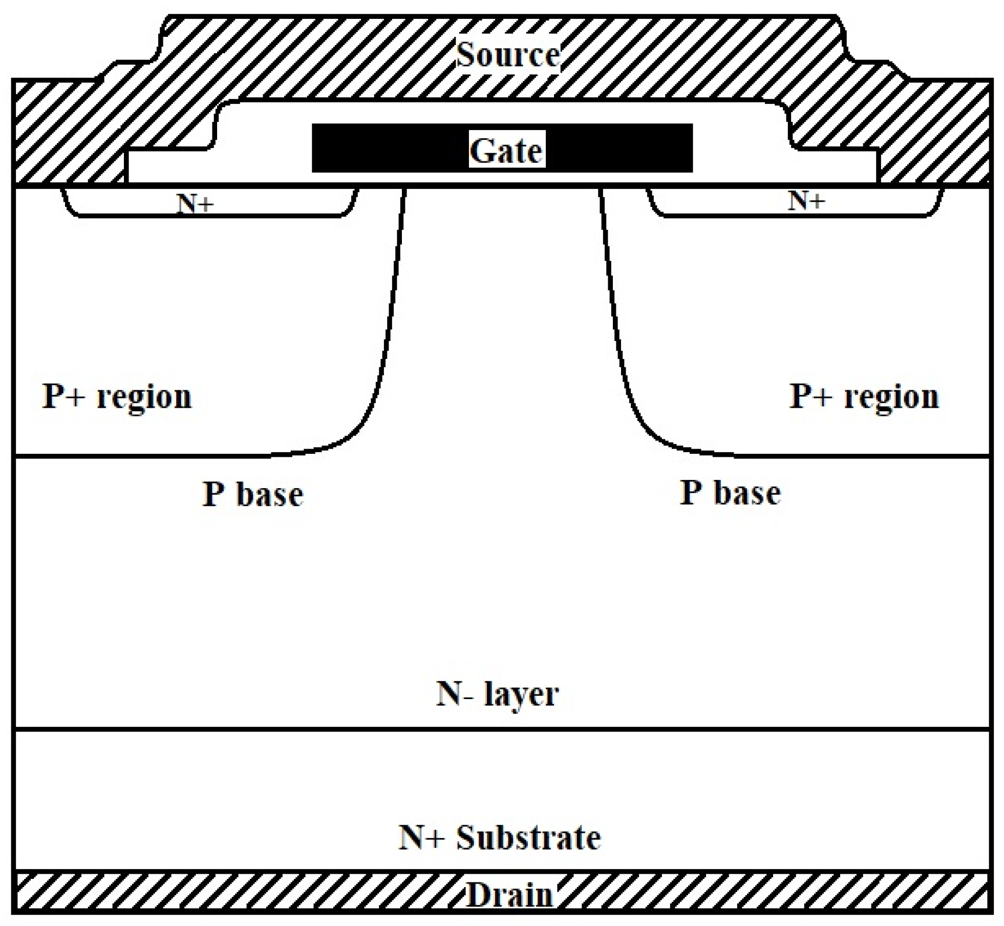
Figure 1. Cross section of a VDMOSFET structure.
Jlpea 11 00033 g001
Figure 2. Half cross section of the VDMOSFET structure.
Jlpea 11 00033 g002
Figure 3. Log of norm of the current density under normal operation of Si (left) and AlGaN (right) VDMOSFET structures at VDS = 40 V and VGS = 20 V.
Jlpea 11 00033 g003
Figure 4. Temperatures under normal operation of Si (left) and AlGaN (right) VDMOSFET structures at VDS = 40 V and VGS = 20 V.
Jlpea 11 00033 g004
Figure 5. Temperatures and log of norm of current densities under electrical breakdown of Si (left) and AlGaN (right) VDMOSFETs at VDS = 40 V and VGS = 20 V.
Jlpea 11 00033 g005
Figure 6. Average Temperatures under normal operation of Si (left) and AlGaN (right) VDMOSFET structures.
Jlpea 11 00033 g006
Figure 7. Maximum Temperatures under normal operation of Si (left) and AlGaN (right) VDMOSFET structures.
Jlpea 11 00033 g007
Figure 8. Drain power for Si (left) and AlGaN (right) VDMOSFET structures.
Jlpea 11 00033 g008
Figure 9. Maximum Temperatures under electrical breakdown of Si (left) and AlGaN (right) VDMOSFET structures.
Jlpea 11 00033 g009
Figure 10. Six-pack Si MOSFET module 3D view (left) and yz-plane view (right).
Jlpea 11 00033 g010
Figure 11. Modified H5 tranformerless topology.
Jlpea 11 00033 g011
Figure 12. Switching sequence for the modified H5 inverter topology.
Jlpea 11 00033 g012
Figure 13. Six-pack AlGaN/GaN HEMT module 3D view (left) and yz-plane view (right).
Jlpea 11 00033 g013
Figure 14. Heatsink for the Si (left) and GaN/AlGaN (right) models.
Jlpea 11 00033 g014
Figure 15. Temperature profile of Si MOSFET (left) and the AlGaN/GaN (right) HEMT modules with the heatsinks not visible.
Jlpea 11 00033 g015
Figure 16. Temperature profile of Si MOSFET (left) and the AlGaN/GaN (right) HEMT modules with the heatsinks visible.
Jlpea 11 00033 g016
Table 1. Material properties of Si and AlGaN.
PropertyNameUnitSiAlGaN
Relative Permittivityεr111.79.7
Thermal ConductivitykW/(m·K)13150
Densityρkg/m323296070
Heat Capacity at constant pressureCpJ/(kg·°C)700490
Electron Lifetimeτnμs100.01
Hole Lifetimeτpμs100.01
Band gapEg0V1.123.7
Electron Affinityχ0V4.054.1
Effective Density of states, valence bandNvcm−3T3/2 × 2.0 × 1015T3/2 × 8 × 1015
Effective Density of states, conduction bandNccm−3T3/2 × 5.3 × 1015T3/2 × 2.3 × 1014
Electron Mobilityμncm2/(V·s)14501000
Hole Mobilityμpcm2/(V·s)500350
Table 2. Thermal properties of materials used for heatsink modeling.
PropertySymbolUnitCuSAC396AlNSiAlGaNAl
Densityρkg/m3896074003260232960702700
Heat capacity at constant pressureCpJ/(kg·K)385220740700490900
Thermal conductivitykW/(m·K)40061.116013150238
Publisher’s Note: MDPI stays neutral with regard to jurisdictional claims in published maps and institutional affiliations.