

Exploring Topological Semi-Metals for Interconnects

 , and
, and
Abstract
:1. Introduction
2. Methodology
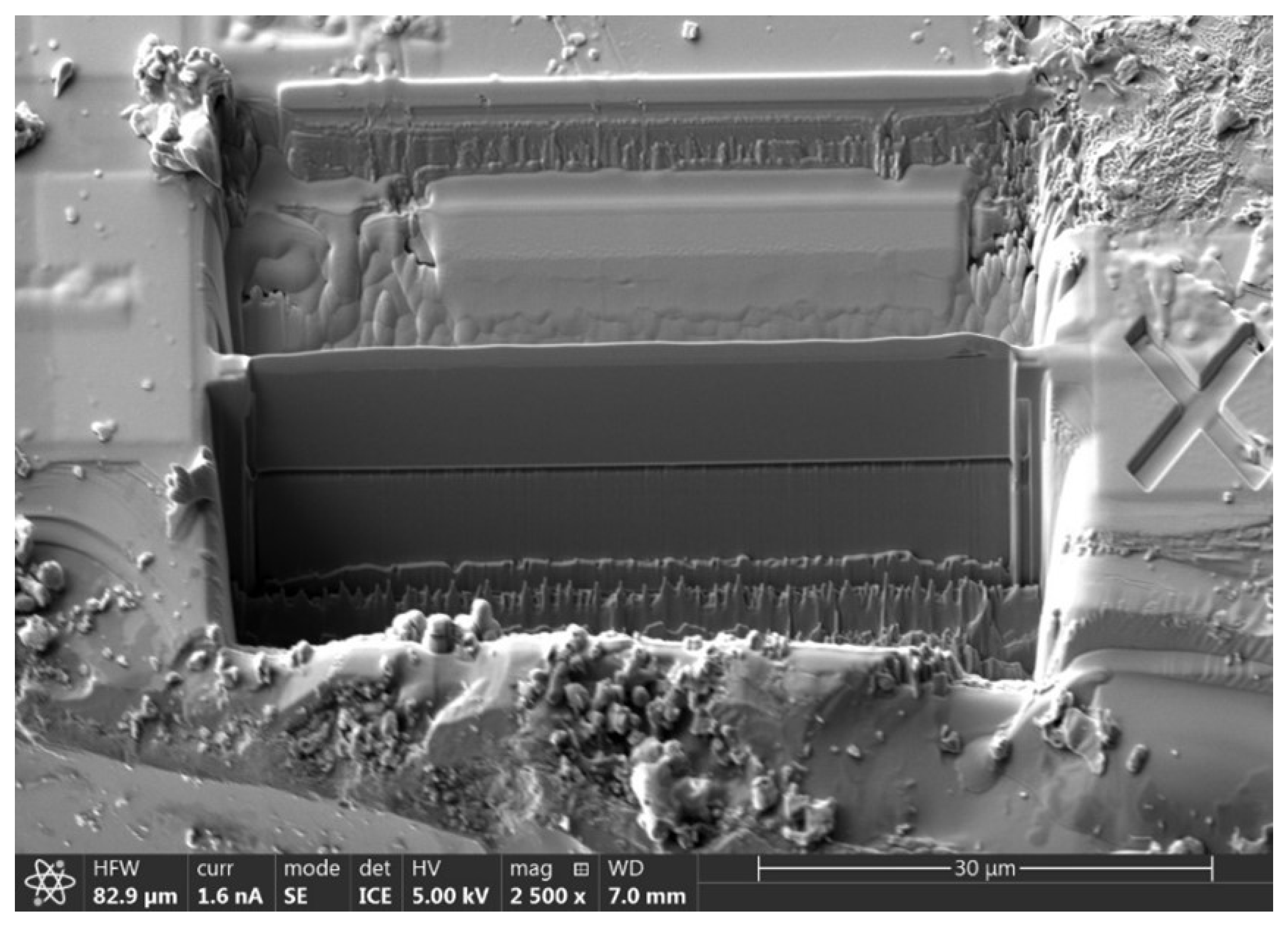
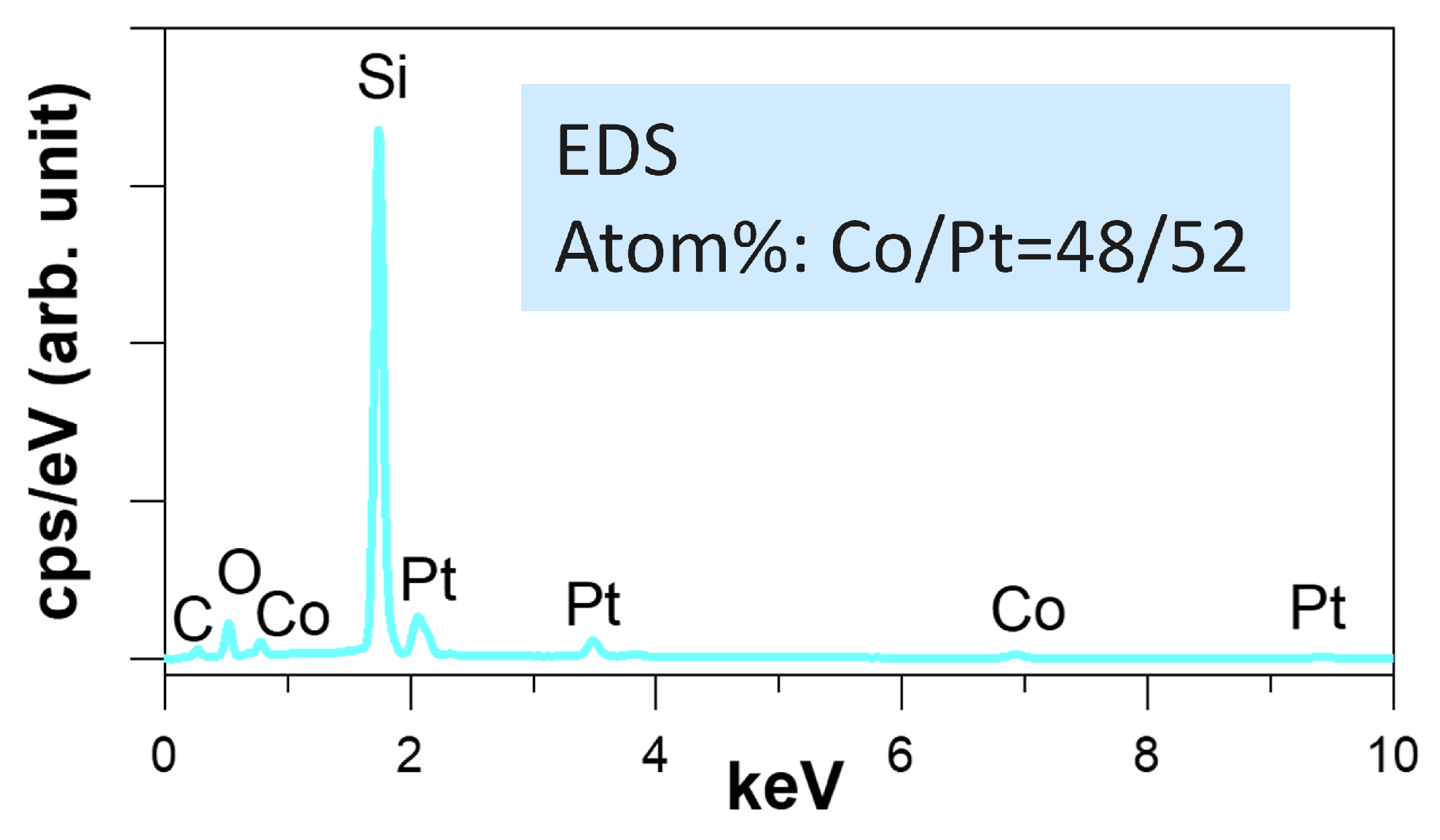
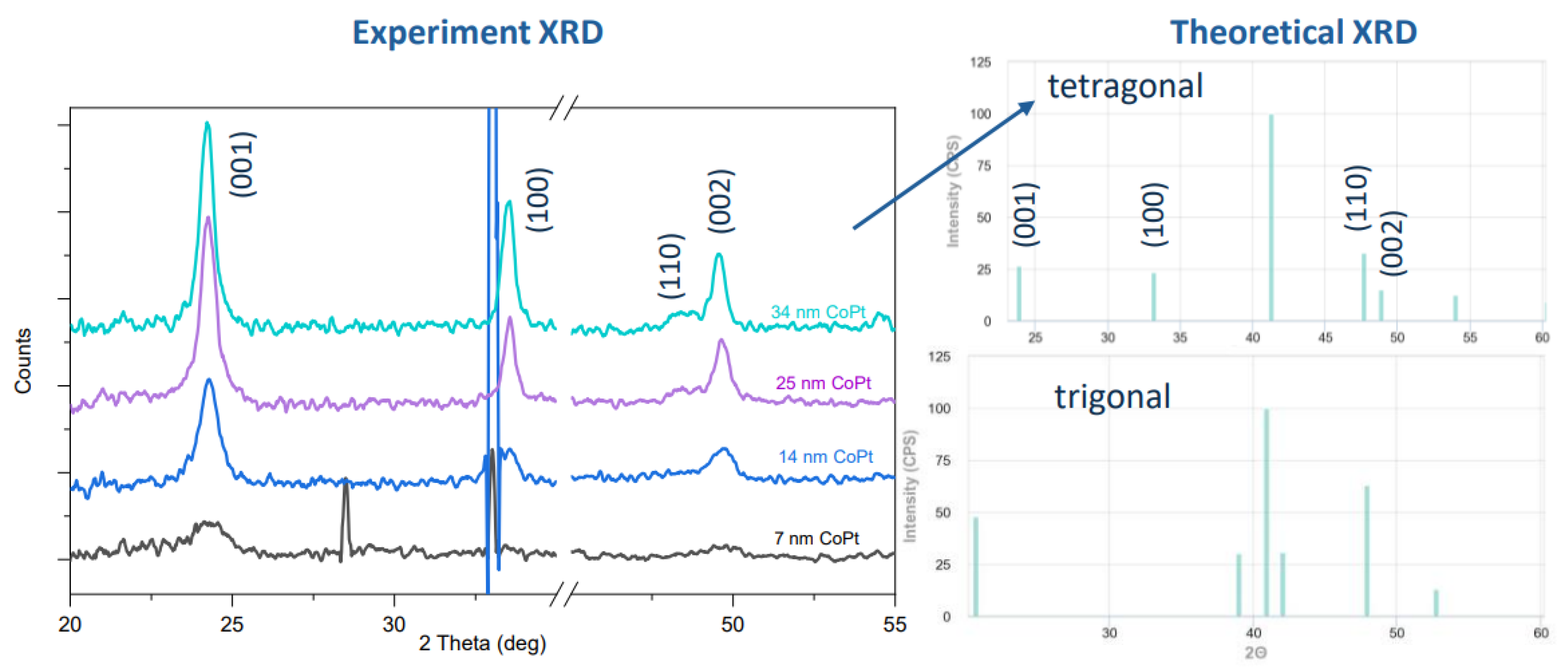
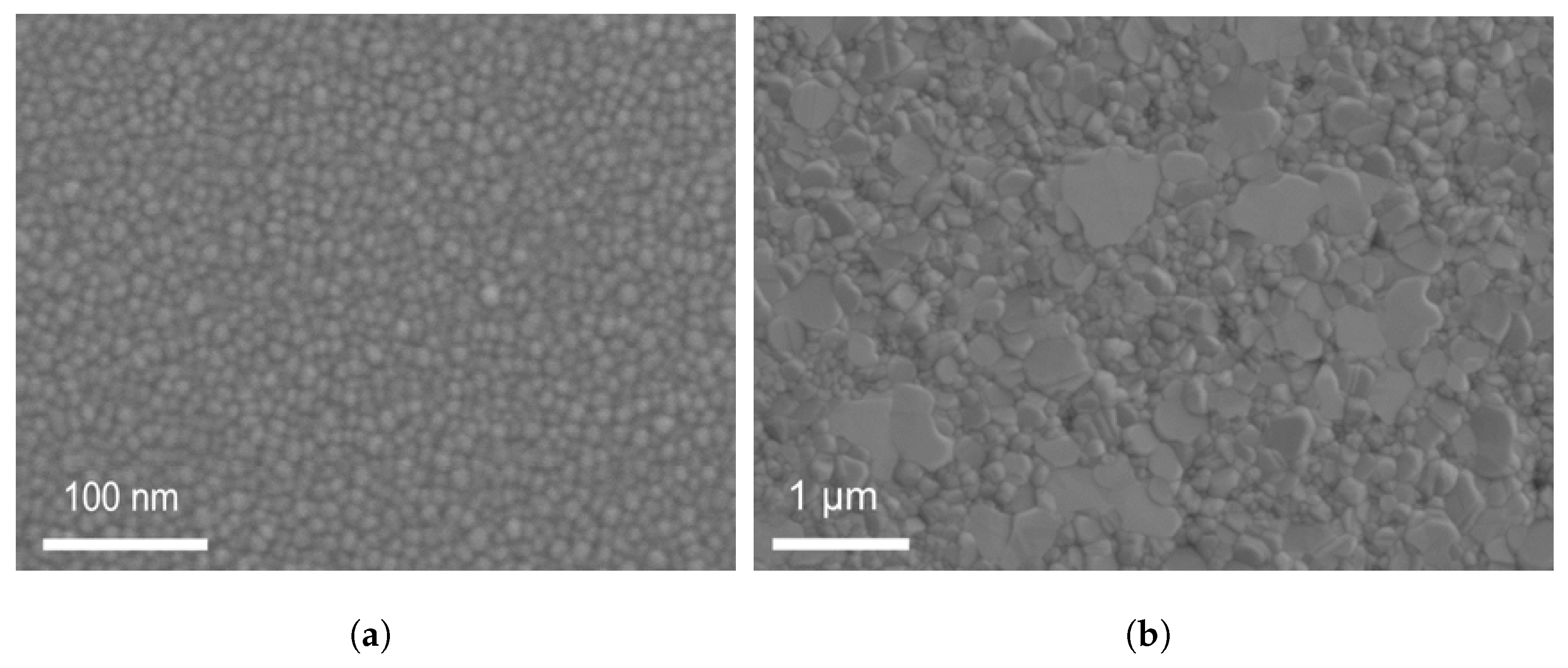
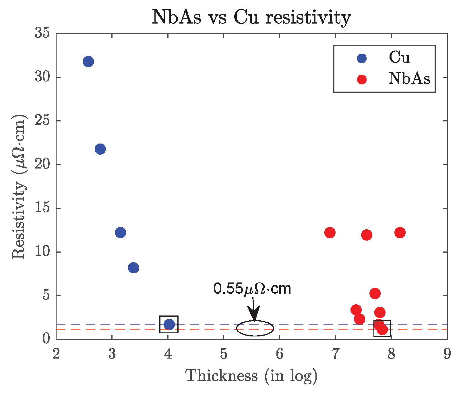
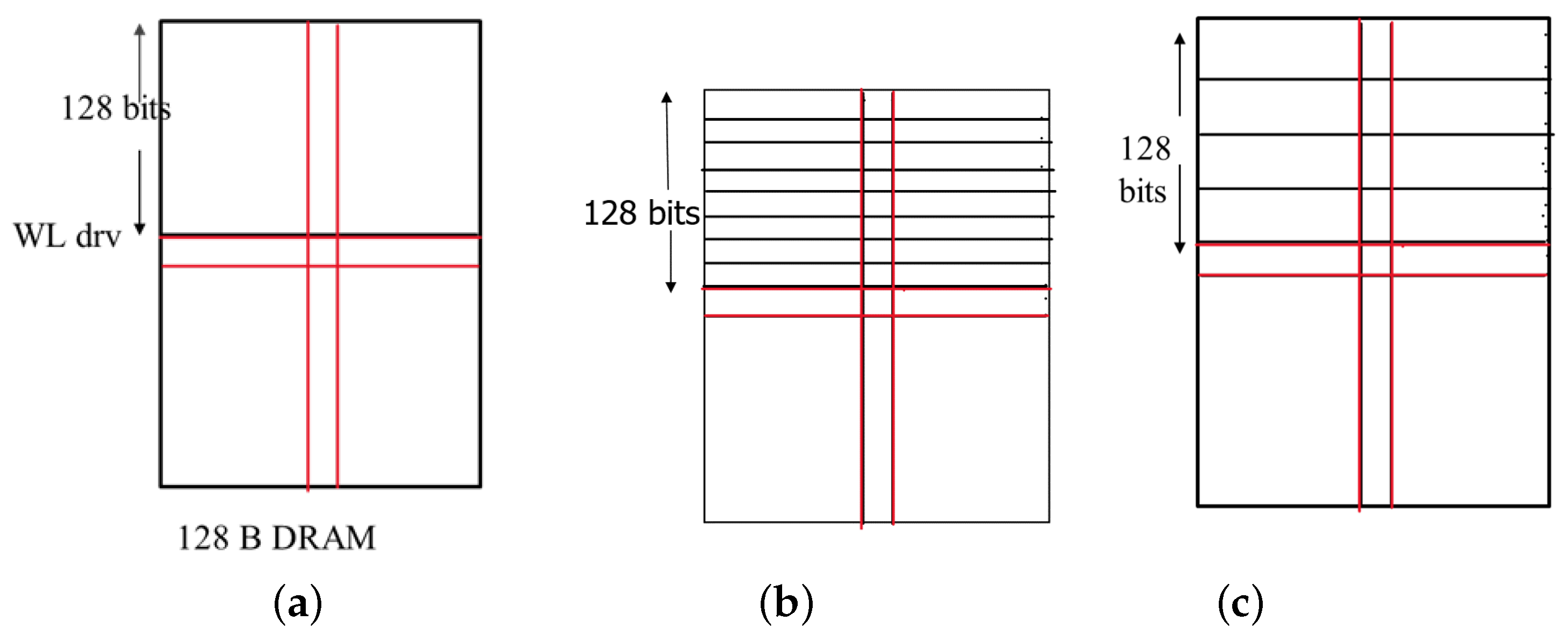
2.1. CoPt Fabrication
2.2. Low-Level Interconnect
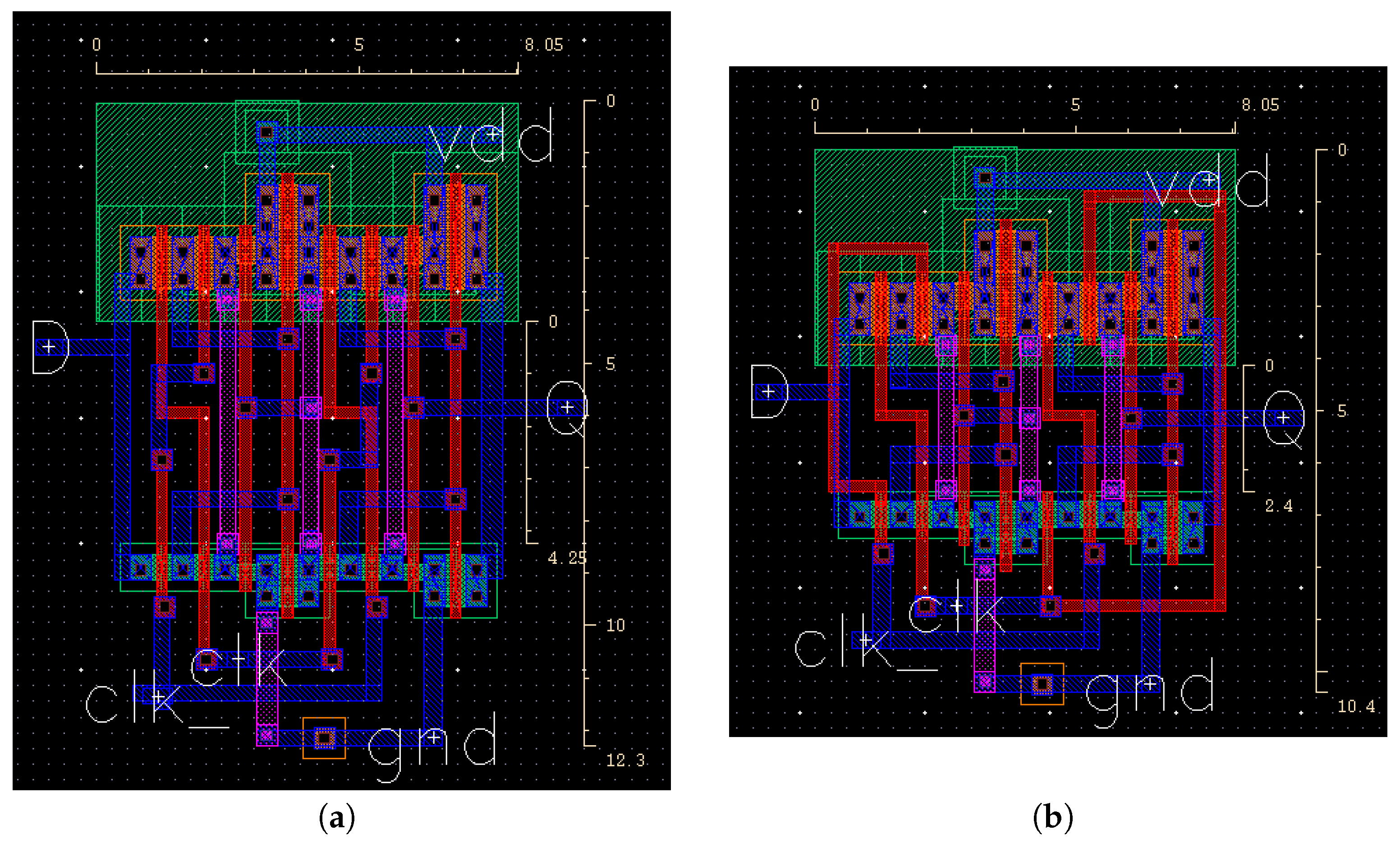
2.3. High-Level Interconnect
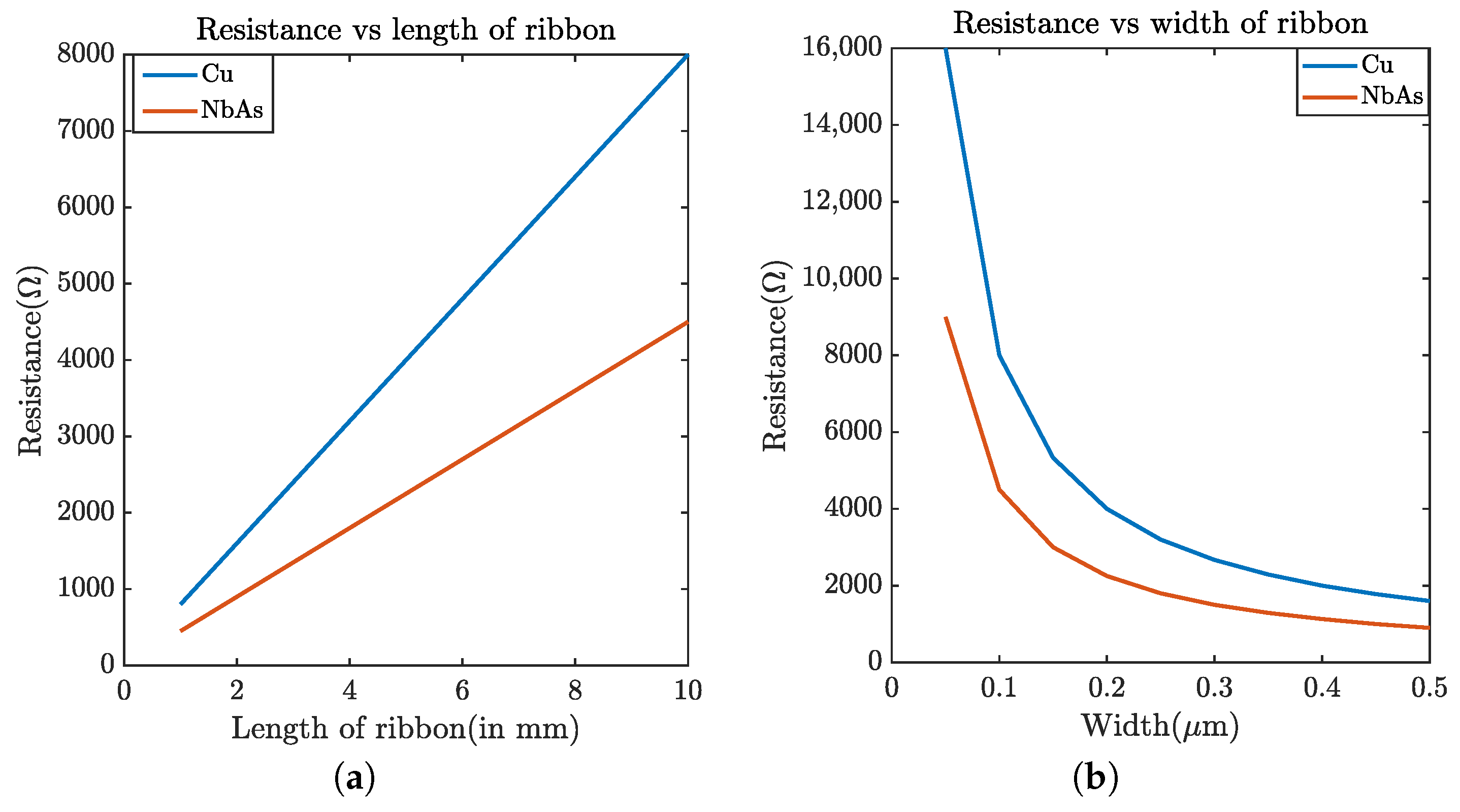
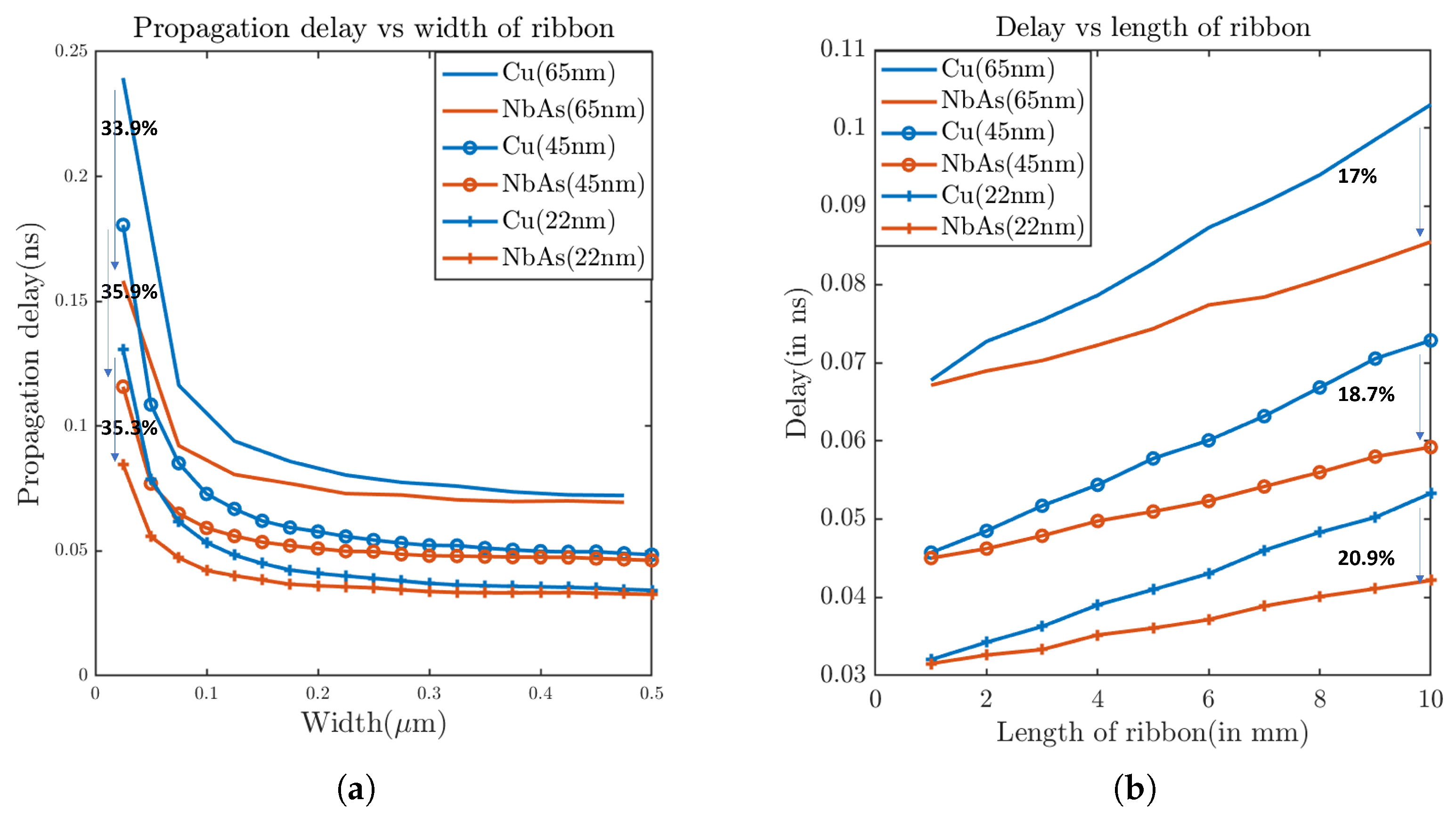
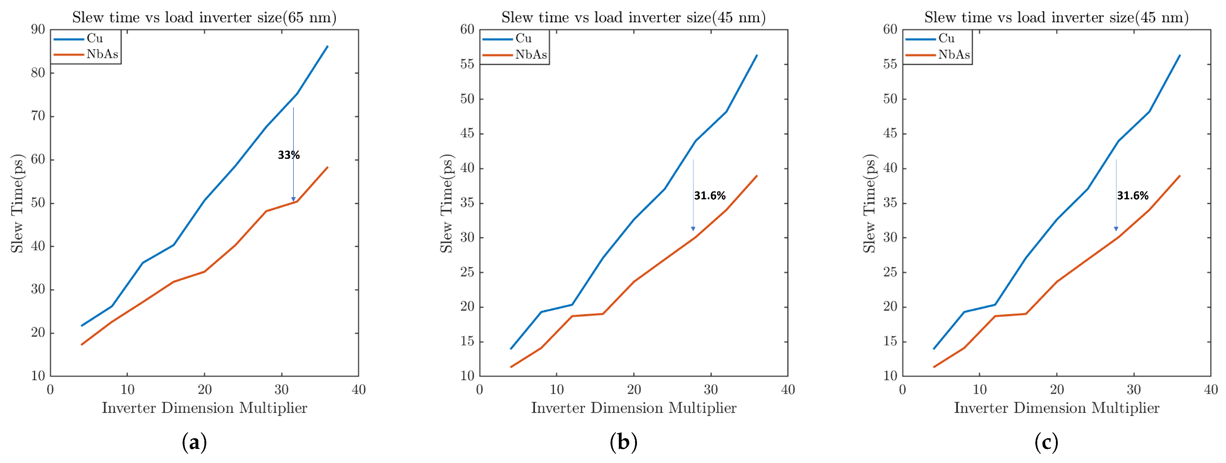
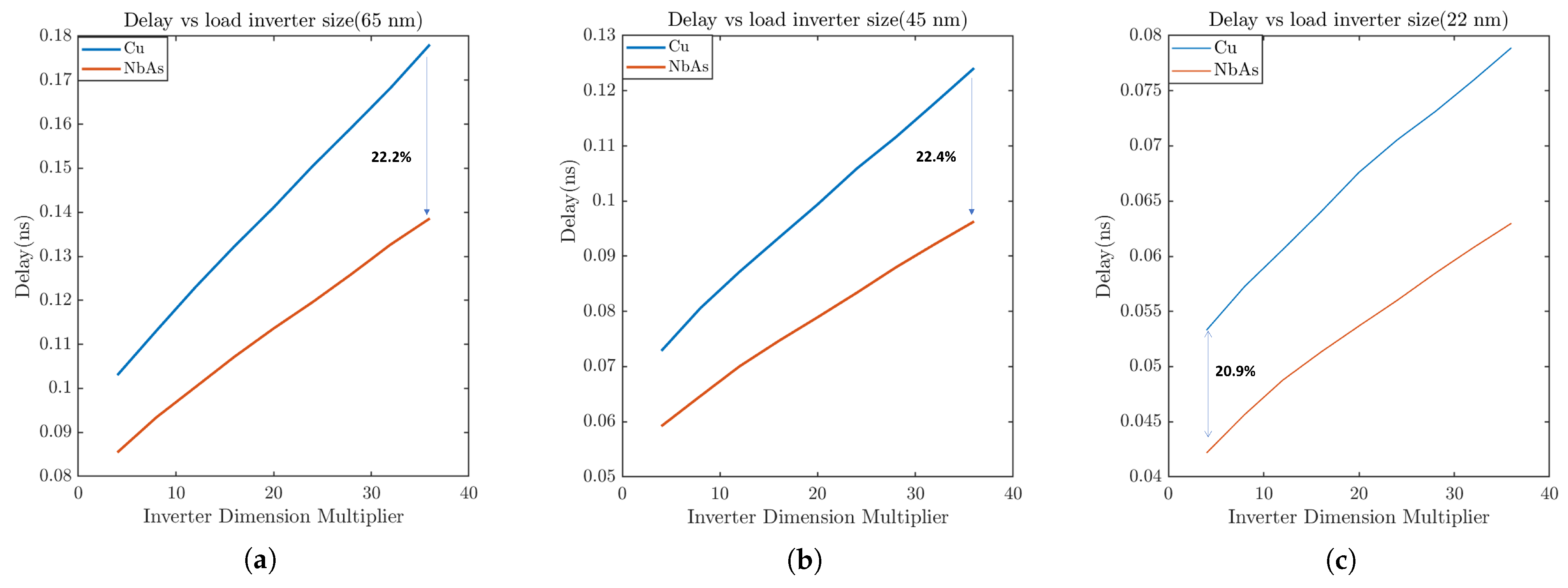
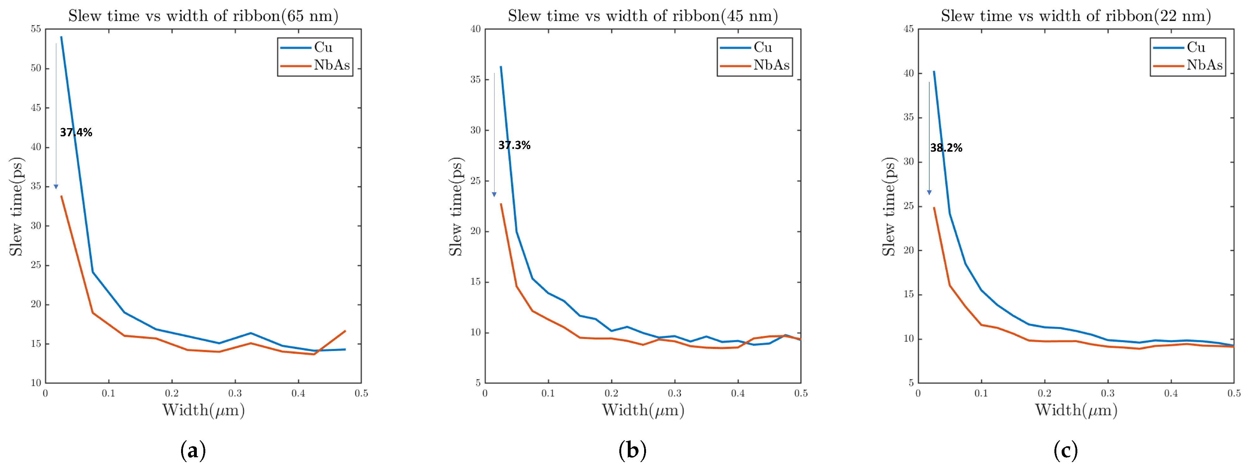
3. Evaluation
3.1. Setup
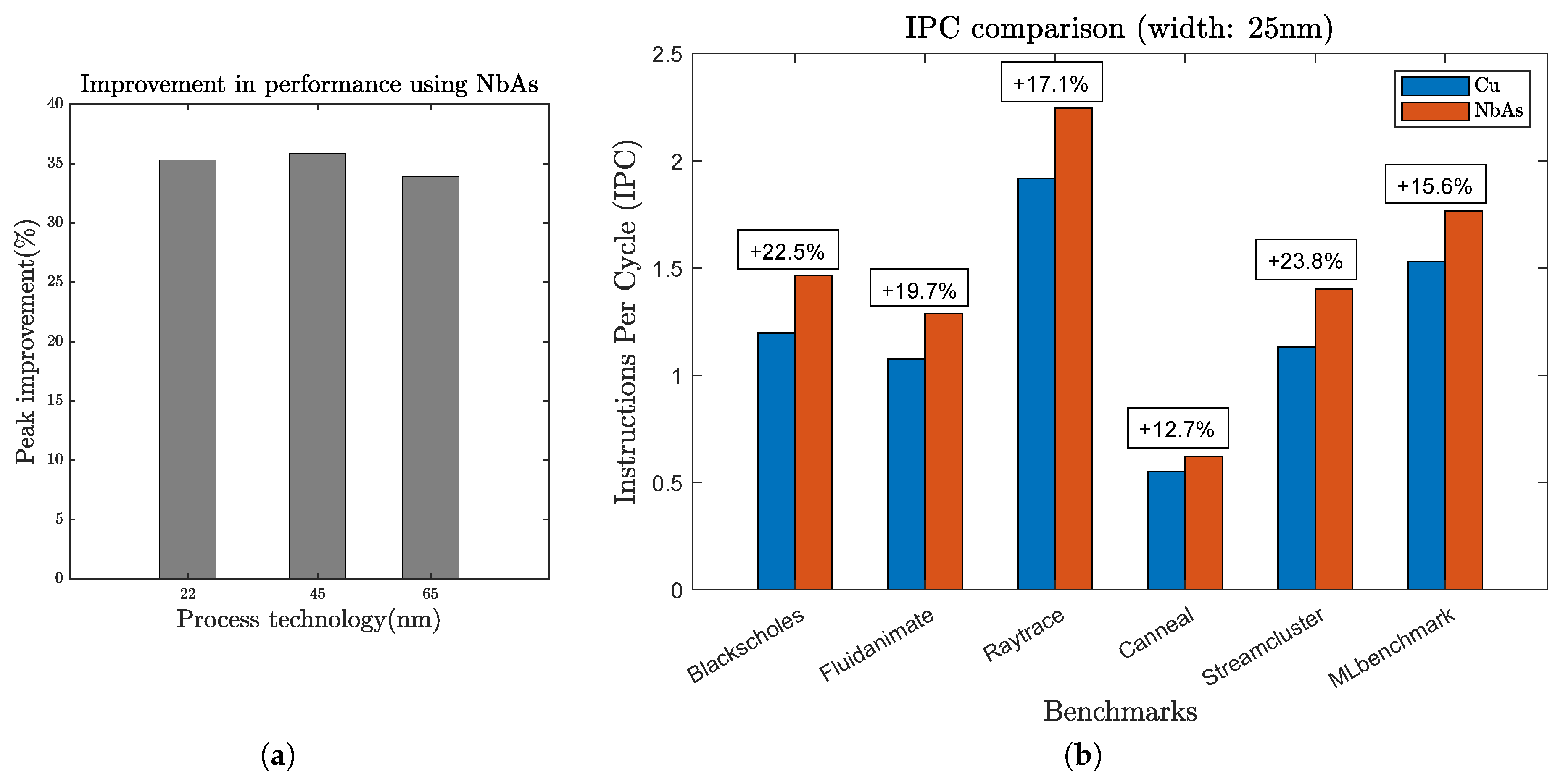
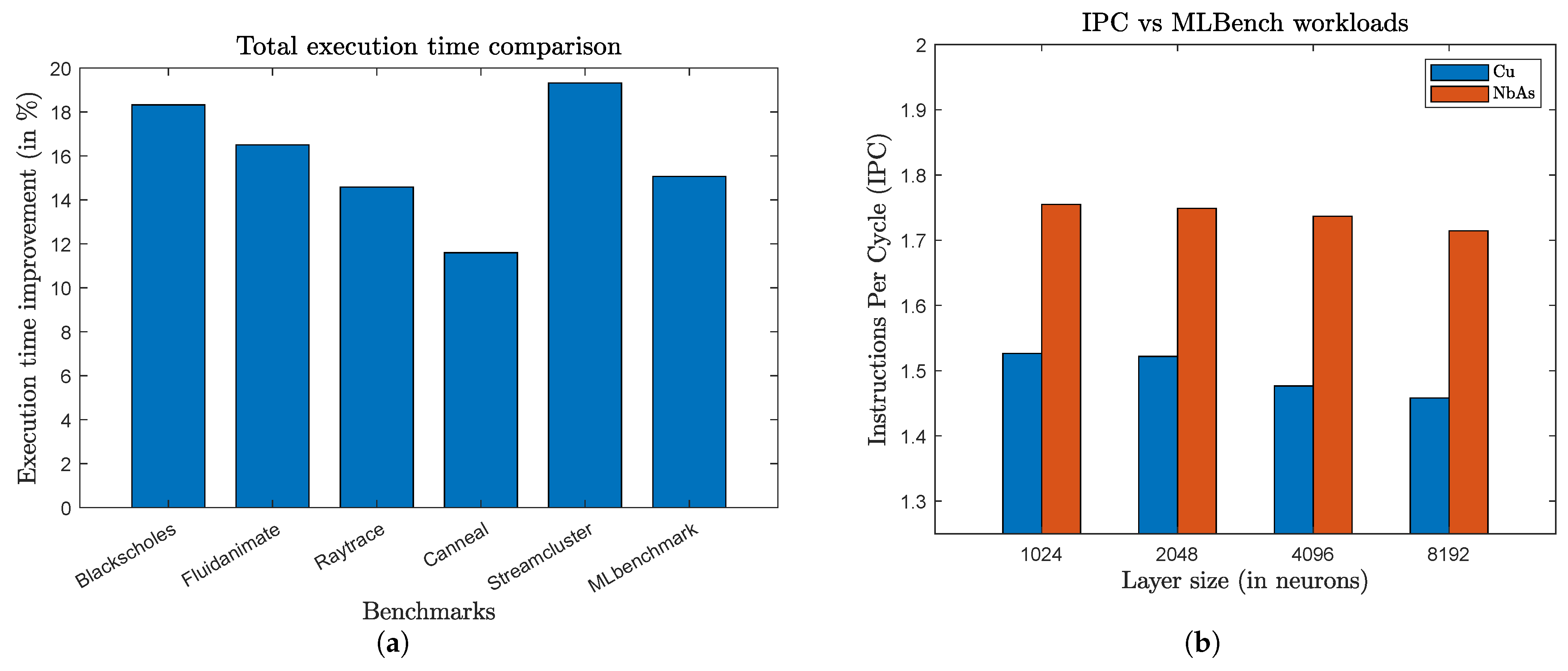
3.2. Results
4. Conclusions
Author Contributions
Funding
Data Availability Statement
Acknowledgments
Conflicts of Interest
References
- Xu, S.Y.; Belopolski, I.; Alidoust, N.; Neupane, M.; Bian, G.; Zhang, C.; Sankar, R.; Chang, G.; Yuan, Z.; Lee, C.C.; et al. Discovery of a Weyl fermion semimetal and topological Fermi arcs. Science 2015, 349, 613–617. [Google Scholar] [CrossRef]
- Jia, S.; Xu, S.Y.; Hasan, M.Z. Weyl semimetals, Fermi arcs and chiral anomalies. Nat. Mater. 2016, 15, 1140–1144. [Google Scholar] [CrossRef]
- Hasan, M.Z.; Xu, S.Y.; Belopolski, I.; Huang, S.M. Discovery of Weyl fermion semimetals and topological Fermi arc states. Annu. Rev. Condens. Matter Phys. 2017, 8, 289–309. [Google Scholar] [CrossRef]
- Karlsruhe, F. ICSD. 2021. Available online: https://icsd.fiz-karlsruhe.de/search/basic.xhtml (accessed on 1 January 2020).
- Xu, S.Y.; Alidoust, N.; Chang, G.; Lu, H.; Singh, B.; Belopolski, I.; Sanchez, D.S.; Zhang, X.; Bian, G.; Zheng, H.; et al. Discovery of Lorentz-violating type II Weyl fermions in LaAlGe. Sci. Adv. 2017, 3, e1603266. [Google Scholar] [CrossRef] [PubMed]
- Chang, G.; Xu, S.Y.; Sanchez, D.S.; Huang, S.M.; Lee, C.C.; Chang, T.R.; Bian, G.; Zheng, H.; Belopolski, I.; Alidoust, N.; et al. A strongly robust type II Weyl fermion semimetal state in Ta3S2. Sci. Adv. 2016, 2, e1600295. [Google Scholar] [CrossRef]
- Lv, B.; Xu, N.; Weng, H.; Ma, J.; Richard, P.; Huang, X.; Zhao, L.; Chen, G.; Matt, C.; Bisti, F.; et al. Observation of Weyl nodes in TaAs. Nat. Phys. 2015, 11, 724–727. [Google Scholar] [CrossRef]
- Niemann, A.C.; Gooth, J.; Wu, S.C.; Bäßler, S.; Sergelius, P.; Hühne, R.; Rellinghaus, B.; Shekhar, C.; Süß, V.; Schmidt, M.; et al. Chiral magnetoresistance in the Weyl semimetal NbP. Sci. Rep. 2017, 7, 43394. [Google Scholar] [CrossRef] [PubMed]
- Lowe-Power, J.; Ahmad, A.M.; Akram, A.; Alian, M.; Amslinger, R.; Andreozzi, M.; Armejach, A.; Asmussen, N.; Beckmann, B.; Bharadwaj, S.; et al. The gem5 simulator: Version 20.0+. arXiv, 2020; arXiv:2007.03152. [Google Scholar]
- Binkert, N.; Beckmann, B.; Black, G.; Reinhardt, S.K.; Saidi, A.; Basu, A.; Hestness, J.; Hower, D.R.; Krishna, T.; Sardashti, S.; et al. The gem5 simulator. ACM SIGARCH Comput. Archit. News 2011, 39, 1–7. [Google Scholar] [CrossRef]
- Li, J.; Ndai, P.; Goel, A.; Salahuddin, S.; Roy, K. Design paradigm for robust spin-torque transfer magnetic RAM (STT MRAM) from circuit/architecture perspective. IEEE Trans. Very Large Scale Integr. (VLSI) Syst. 2009, 18, 1710–1723. [Google Scholar] [CrossRef]
- Apple. Apple Unleashes M1. 2020. Available online: https://www.apple.com/newsroom/2020/11/apple-unleashes-m1 (accessed on 1 July 2022).
- Arizona State University Predictive Technology Model (PTM). 2008. Available online: http://ptm.asu.edu/ (accessed on 10 September 2022).
- Gall, D.; Cha, J.J.; Chen, Z.; Han, H.J.; Hinkle, C.; Robinson, J.A.; Sundararaman, R.; Torsi, R. Materials for interconnects. MRS Bull. 2021, 46, 959–966. [Google Scholar] [CrossRef]
- Butko, A.; Garibotti, R.; Ost, L.; Sassatelli, G. Accuracy evaluation of gem5 simulator system. In Proceedings of the 7th International Workshop on Reconfigurable and Communication-Centric Systems-on-Chip (ReCoSoC), York, UK, 9–11 July 2012; IEEE: New York, NY, USA, 2012; pp. 1–7. [Google Scholar]
- Bienia, C.; Kumar, S.; Singh, J.P.; Li, K. The PARSEC benchmark suite: Characterization and architectural implications. In Proceedings of the 17th International Conference on Parallel Architectures and Compilation Techniques, Toronto, ON, Canada, 25–29 October 2008; pp. 72–81. [Google Scholar]
- Meister, K. ML Benchmark. 2020. Available online: https://github.com/kmeister/ML_Benchmark#2-install-the-riscv-toolchain (accessed on 10 June 2022).
- Péneau, P.Y.; Bruguier, F.; Novo, D.; Sassatelli, G.; Gamatié, A. Towards a Flexible and Comprehensive Evaluation Approach for Adressing NVM Integration in Cache Hierarchy. 2021. Available online: https://hal-lirmm.ccsd.cnrs.fr/lirmm-03341602 (accessed on 10 November 2022).
- Shen, J.P.; Lipasti, M.H. Modern Processor Design: Fundamentals of Superscalar Processors; Waveland Press: Long Grove, IL, USA, 2013. [Google Scholar]
- Eeckhout, L. Computer architecture performance evaluation methods. Synth. Lect. Comput. Archit. 2010, 5, 1–145. [Google Scholar]


| Parameter | Value |
|---|---|
| ISA | x86 |
| CPU | DerivO3CPU |
| CPU model | Out-of-order |
| Core frequency | 2 GHz |
| Cores | 1 |
| L1-I size | 64 kB |
| L1-D size | 128 kB |
| L1 associativity | 2 |
| L1 latency | 4 |
| L2 size | 2048 kB |
| L2 associativity | 8 |
| L2 latency | 15 |
| Cacheline size | 64 B |
| Design | Delay | % Benefit |
|---|---|---|
| Poly-256B | 530.4 ps | 66.6% |
| Poly-WSM-256B | 177 ps | |
| Polystrapping-256B-(WL1-WL16) | 32.7 ps | 8.56% |
| Poly + WSM-strapping-256B-(WL1-WL16) | 29.9 ps | |
| Polystrapping-256B-(WL1-WL32) | 43.8 ps | 25.57% |
| Poly + WSM-strapping-256B-(WL1-WL32) | 32.6 ps | |
| Poly-512B | 1289 ps | 65.7% |
| Poly-WSM-512B | 442 ps | |
| Polystrapping-512B-(WL1-WL16) | 126.9 ps | 7.01% |
| Poly + WSM-strapping-512B-(WL1-WL16) | 118 ps | |
| Polystrapping-512B-(WL1-WL32) | 136.9 ps | 12.34% |
| Poly + WSM-strapping-512B-(WL1-WL32) | 120 ps |
| Regular Layout | Using Poly (1 μm) | Using Poly + WSM | |
|---|---|---|---|
| D to Q | 0.1 ns | 0.35 ns | 0.21 ns |
| Clk to Q | 0.05 ns | 0.28 ns | 0.12 ns |
| Parameter | Value |
|---|---|
| Length | 10 mm |
| Width | 0.025 μm |
| Aspect ratio | 8:1 |
| Resistivity (Cu) | 1.6 μΩ·cm |
| Resistivity (NbAs) | 0.9 μΩ·cm |
| Resistivity (Poly) | 2 μΩ·cm |
| Benchmark | Memory Usage (in kB) | L2 Miss Rate |
|---|---|---|
| Blackscholes | 698 | 0.20 |
| Fluidanimate | 735 | 0.63 |
| Raytrace | 820 | 0.77 |
| Canneal | 741 | 0.42 |
| Streamcluster | 730 | 0.88 |
| NN Layer Sizes (in Neurons) | Memory Usage (in kB) |
|---|---|
| 512 | 668 |
| 1024 | 673 |
| 2048 | 687 |
| 4096 | 742 |
| 8192 | 951 |
Disclaimer/Publisher’s Note: The statements, opinions and data contained in all publications are solely those of the individual author(s) and contributor(s) and not of MDPI and/or the editor(s). MDPI and/or the editor(s) disclaim responsibility for any injury to people or property resulting from any ideas, methods, instructions or products referred to in the content. |
© 2023 by the authors. Licensee MDPI, Basel, Switzerland. This article is an open access article distributed under the terms and conditions of the Creative Commons Attribution (CC BY) license (https://creativecommons.org/licenses/by/4.0/).
Share and Cite
Kundu, S.; Roy, R.; Rahman, M.S.; Upadhyay, S.; Topaloglu, R.O.; Mohney, S.E.; Huang, S.; Ghosh, S. Exploring Topological Semi-Metals for Interconnects. J. Low Power Electron. Appl. 2023, 13, 16. https://doi.org/10.3390/jlpea13010016
Kundu S, Roy R, Rahman MS, Upadhyay S, Topaloglu RO, Mohney SE, Huang S, Ghosh S. Exploring Topological Semi-Metals for Interconnects. Journal of Low Power Electronics and Applications. 2023; 13(1):16. https://doi.org/10.3390/jlpea13010016
Chicago/Turabian StyleKundu, Satwik, Rupshali Roy, M. Saifur Rahman, Suryansh Upadhyay, Rasit Onur Topaloglu, Suzanne E. Mohney, Shengxi Huang, and Swaroop Ghosh. 2023. "Exploring Topological Semi-Metals for Interconnects" Journal of Low Power Electronics and Applications 13, no. 1: 16. https://doi.org/10.3390/jlpea13010016
APA StyleKundu, S., Roy, R., Rahman, M. S., Upadhyay, S., Topaloglu, R. O., Mohney, S. E., Huang, S., & Ghosh, S. (2023). Exploring Topological Semi-Metals for Interconnects. Journal of Low Power Electronics and Applications, 13(1), 16. https://doi.org/10.3390/jlpea13010016