

CMOS Design of Chaotic Systems Using Biquadratic OTA-C Filters
by
 and
and
Eduardo Juarez-Mendoza
†,
Francisco Asahel del Angel-Diaz
†,
Alejandro Diaz-Sanchez
† and
Esteban Tlelo-Cuautle
*,†
Department of Electronics, INAOE, Tonantzintla, Puebla 72840, Mexico
*
Author to whom correspondence should be addressed.
†
These authors contributed equally to this work.
J. Low Power Electron. Appl. 2024, 14(1), 14; https://doi.org/10.3390/jlpea14010014
Submission received: 5 October 2023
/
Revised: 15 December 2023
/
Accepted: 2 March 2024
/
Published: 4 March 2024
Abstract
:This manuscript shows the CMOS design of Lorenz systems using operational transconductance amplifiers (OTAs). Two Lorenz systems are then synchronized in a master–slave topology and used to implement a CMOS secure communication system. The contribution is devoted to the correct design of first- and second-order OTA-C filters, using 180 nm CMOS technology, to guarantee chaotic behavior. First, Simulink is used to simulate a secure communication system using two Lorenz systems connected in a master–slave topology, which is tested using sinusoidal signals that are masked by chaotic signals. Second, the Lorenz systems are scaled to have amplitudes of the state variables below 1 Volt, to allow for CMOS design using OTA-C filters. The transconductances of the OTAs are tuned to accomplish a Laplace transfer function. In this manner, this work highlights the design of a second-order CMOS OTA-C filter, whose damping factor is tuned to generate appropriate chaotic behavior. Finally, chaotic masking is performed by designing a whole CMOS secure communication system by using OTA-C based Lorenz systems, and its SPICE simulation results show its appropriateness for hardware security applications.
1. Introduction
Chaos is a complex and seemingly disordered phenomenon that was introduced by meteorologist Edward Lorenz in proposing a mathematical model consisting of three ordinary differential equations (ODEs) [1]. Up to now, researchers know that a chaotic system is highly sensitive to slight variations in the initial conditions, which can lead the solutions of ODEs to have completely different trajectories over time. In this manner, despite its apparent disorder, chaos has at least three remarkable characteristics, i.e., high sensitivity to initial conditions, lack of periodicity, and deterministic behavior, which means that its time evolution is completely determined by its mathematical model. In the continuous-time domain, a chaotic system must have at least three ODEs, as for the case of the Lorenz system [2], which is one of the most famous examples of chaotic systems.
Chaotic systems have proven to be useful in the design of secure communications. For instance, the authors in [3] detail the development of chaos-based digital communication systems, including coherent and non-coherent systems. In this work, a secure communication system is designed by applying the synchronization technique introduced by Pecora and Carroll [4], where two chaotic systems, such as Lorenz systems, can be synchronized to perform a chaotic masking of information. This work uses two Lorenz systems that are synchronized in a master–slave topology to mask data. Additionally, one can use other chaotic systems, for example, the autonomous electronic chaos generator, which comprises a bipolar junction transistor, a resistor, two inductors, and one capacitor [5]; chaotic maps designed with four transistors [6,7]; or other chaotic systems designed with different building blocks using CMOS technology. Examples of the latter include the work in [8], which uses a modified voltage differencing voltage transconductance amplifier; ref. [9], which uses a voltage differencing inverted buffered amplifier; refs. [10,11], which use a modified voltage differencing current conveyor; ref. [12], which uses a current-controlled current conveyor feedback amplifier; ref. [13], which uses a single extra-X current-controlled current conveyor; ref. [14], which uses a voltage differencing gain amplifier; ref. [15], which uses cross-coupled inverter rings; and [16], which uses operational amplifiers and multipliers. Despite the huge number of active devices, this work shows the suitability of operational transconductance amplifiers (OTAs) to design biquadratic filters that are tuned to implement CMOS chaos generators.
The CMOS design of OTAs is not a trivial task, especially when the target is to develop low-voltage and low-power circuit applications. In designing chaos generators, another important device is the CMOS multiplier, for which a good tutorial was introduced by Han and Sanchez-Sinencio [17], where the authors highlight that the multiplier is used not only as a computational building block but also as a programming element in systems such as filters and neural networks, and as a mixer/modulator in communication systems. Regarding OTA design, recent works emphasize its CMOS implementation, as in [18], where an OTA-based meminductor simulator circuit is introduced, or in [19], where a simple realization of the meminductor emulator using two OTAs and two capacitors is presented. In designing chaotic systems, active filters and those implemented with OTAs could be required. Some related works on OTA-C filters are the following: the authors in [20] show two new first-order universal active filter configurations employing OTAs and grounded capacitors; in [21], the authors present a biquadratic filter using one dual-output OTA, three single-output OTAs, and two grounded capacitors to derive a new quadrature oscillator with independent control of the oscillation frequency and the oscillation condition; the authors in [22] present an independently tunable five-input and three-output biquadratic filter using five single-ended output OTAs and two grounded capacitors; and the authors in [23] present an OTA-C filter for biomedical applications that consists of a cascade of biquadratic sections, each configured via a serial-peripheral-interface circuit embedded with nonvolatile memories to provide low-pass or bandpass response. An implementation of an OTA-C filter using commercially available discrete components was given in [24]; an OTA-based filter with low sensitivity operating at high frequency was given in [25]; OTA-based biquadratic filters with electronically reconfigurable transfer functions were given in [26]; and biquadratic OTA-C and universal filters with tunable pole-Q were introduced in [27]. One can find more works related to OTA-C filters, but in all cases, the topologies are quite similar to the ones given in the tutorial [28]. The outstanding challenge is the design of integrated circuits for low-voltage and low-power applications, as in the case studies given in [29,30,31].
The remaining sections are organized as follows: Section 2 shows the mathematical model and analysis of Lorenz systems and synchronization in a master–slave topology using Simulink to appreciate an application in the chaotic masking of sinusoidal signals. Section 3 shows the scaling of the Lorenz system to obtain amplitudes of the state variables within ±1 Volt to allow for CMOS design using 180 nm integrated circuit technology; it also shows the macro-modeling of the OTA-C blocks that implement first- and second-order active filters. Section 4 pays special attention to the design of the OTAs, detailing the tuning of the transconductances, and the design of the OTA-C biquad filters, the damping factor of which is tuned to generate chaotic behavior. Section 5 shows the design of a CMOS secure communication system that synchronizes two CMOS Lorenz systems and masks a sinusoidal signal, which is recovered after having been encrypted by chaotic signals. Finally, the conclusions are provided in Section 6.
2. Chaotic Masking Using Lorenz Systems
In his seminal work [1], Lorenz introduced a mathematical model to describe how the air behaves and evolves in the atmosphere under small changes. This model helped him to discover that chaotic behavior can be modeled by three ODEs and that their solutions highly depend and are highly sensitive to the initial conditions. Since then, such a model has been well known as Lorenz system and its attractor is said to have a butterfly effect. Equation (1) shows the mathematical model of the Lorenz system, which generates chaotic behavior by setting the coefficients as [1] and and by using the initial conditions of = (0.1, 0.1, 0.1).
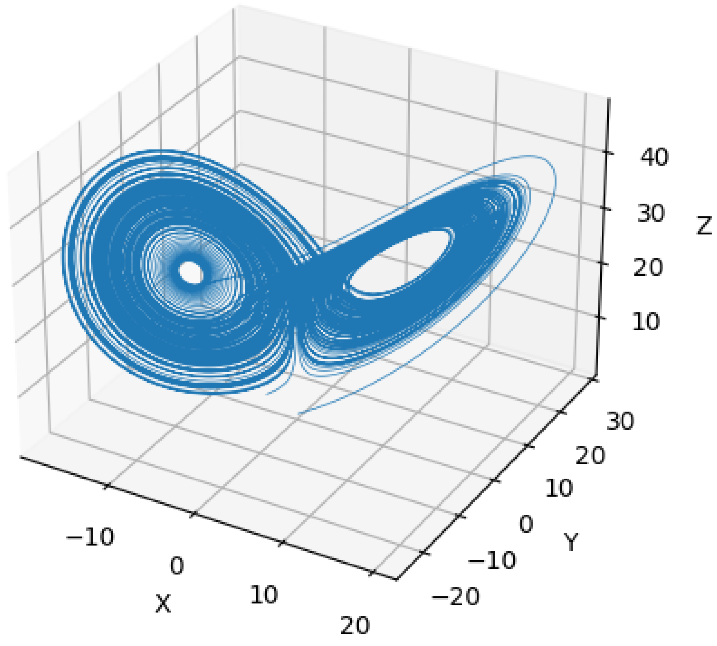
The high-level simulation of the chaotic Lorenz system can be performed by using Simulink, whose equations in the frequency domain are given in (2). The block description is sketched in Figure 1, where it can be appreciated that the equations are synthesized using addition, subtraction, multiplication, and gain blocks, while three integrator blocks are used to obtain each state variable, and . The simulated times series for each state variable can be appreciated in Figure 2, while the chaotic attractor in a 3D space is shown in Figure 3.
Simulink is a useful software application to test the synchronization of two identical chaotic systems. Let us consider two Lorenz systems to perform their synchronization by applying the Pecora and Carroll technique. In this case, a master–slave topology can be synthesized from (3) (denoting the master system) and (4) (denoting the slave system), where it can be appreciated that one of the variables, e.g., , of the master system is used as a coupling signal to control and synchronize the slave system, so that . This coupling signal is adjusted over time to make both systems evolve similarly, thus achieving the synchronization of their chaotic behaviors.
As one can infer, Equations (3) and (4) can be described in Simulink, as shown in Figure 4. The blocks of the master system (m) are distinguished from those of the synchronized slave system (s), but according to (3) and (4), state variable must be taken from the master block, i.e., . As the synchronization is ideal, i.e., using the mathematical equations given in (3) and (4), the phase plots between the state variables of the master and slave systems form a line with a 45° slope. This synchronized scheme can be used to implement a secure communication system, as the one shown in Figure 5.
Chaotic masking by using two synchronized systems in a master–slave topology can be performed as shown in Figure 5. The upper blocks describe the masking of chaos () with the transmitted signal and the recovery of the original signal by subtracting the chaotic time series (). In this case, channel encrypts the transmitted signal (), and the recovered one () must be the same, i.e., . Let us consider a test signal as the sum of three sine waves, as given in (5), to which the chaos of the master system () is added, as given in (6). In this case, channel encrypts the information being transmitted; afterwards, the latter can be recovered by subtracting the chaotic signal in the slave system, with behaving as , thus generating the equation given in (7). In the end, as the master and slave systems are synchronized, , and finally, .
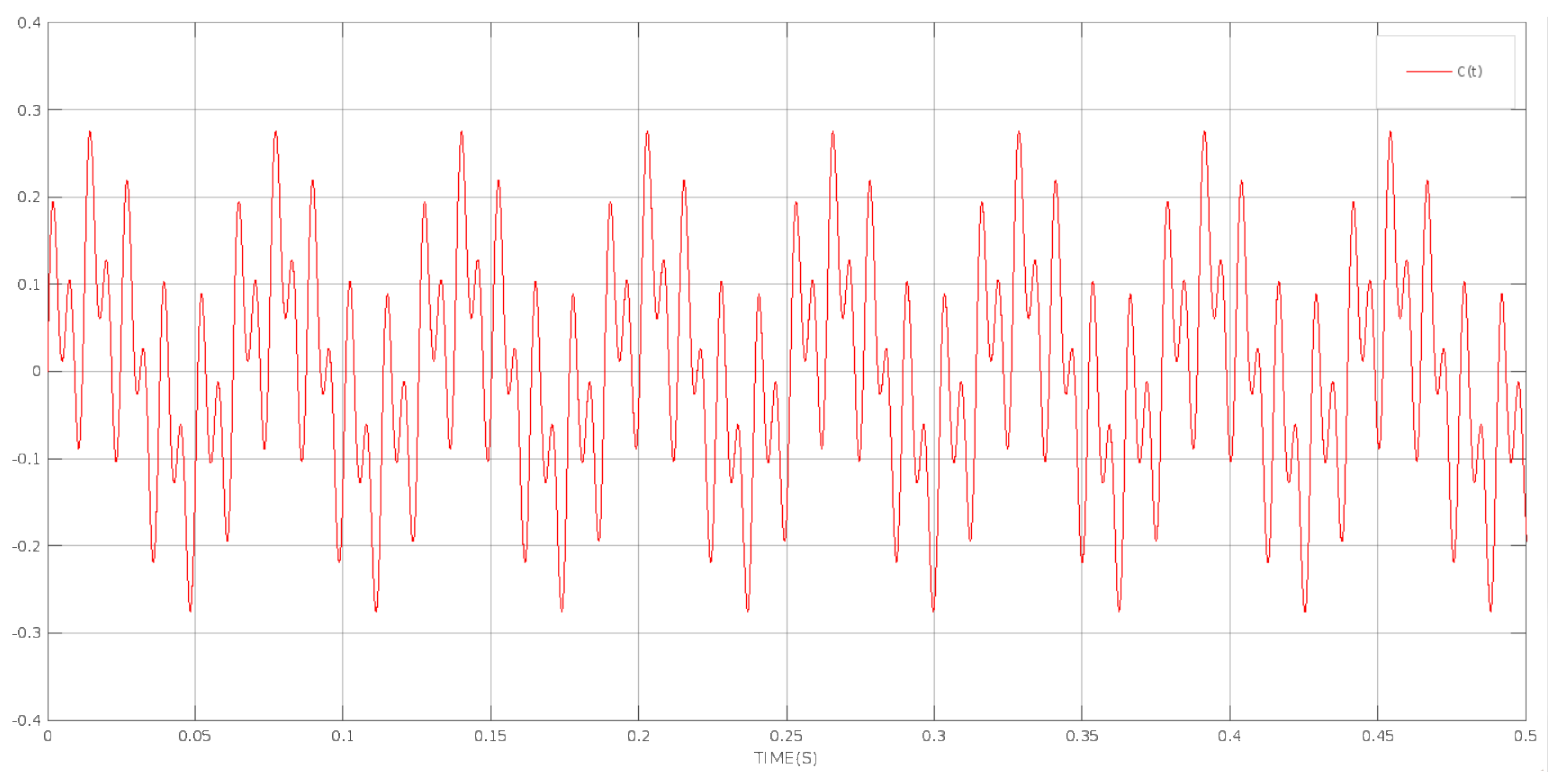
The test signal given in (5), consisting of the sum of three sine signals of different frequencies and equal amplitude, is shown in Figure 6. This signal is masked with chaos, so that the channel is described by (6), as shown in Figure 7. If the slave follows the master system with zero error, then the recovered signal can be expressed by (7), as shown in Figure 8.
3. Scaling of Lorenz System and Simulation Using OTA-C Filters
The CMOS design using integrated circuit technology imposes restrictions on the amplitudes of the signals. In this work, Lorenz systems are designed using 180 nm integrated circuit technology from UMC. Both MOSFET models of the P- and N-channels are nm180_reg_18_V124 of level 49. In this manner, the mathematical model is scaled to have amplitudes of the state variables within a range of ±1 Volt. In principle, the scaling process is performed by a variable change for each state variable, until one finds the updated coefficient values that allow for CMOS design. In this work, the scaled system of equations for Lorenz systems in the Laplace domain is given in (8). One can see that the Laplace transform of the multiplication of two variables in the time domain produces the convolution of those variables; in this case, the two products are described by and .
From this system of equations, the manipulation of each state variable can lead to associate transfer functions to first- and second-order (biquadratic) active filters. For the case of state variable , it can be associated to a first-order low-pass filter, as shown in (9).
For the case of , it also results in associating low-pass filters that multiply one state variable or the convolution of two of them, as shown in (10).
For the case of , one can associate (11). However, as is given in (9), one can derive an equation that includes a transfer function equivalent to a biquadratic active filter, as given in (12), which also performs the convolution .
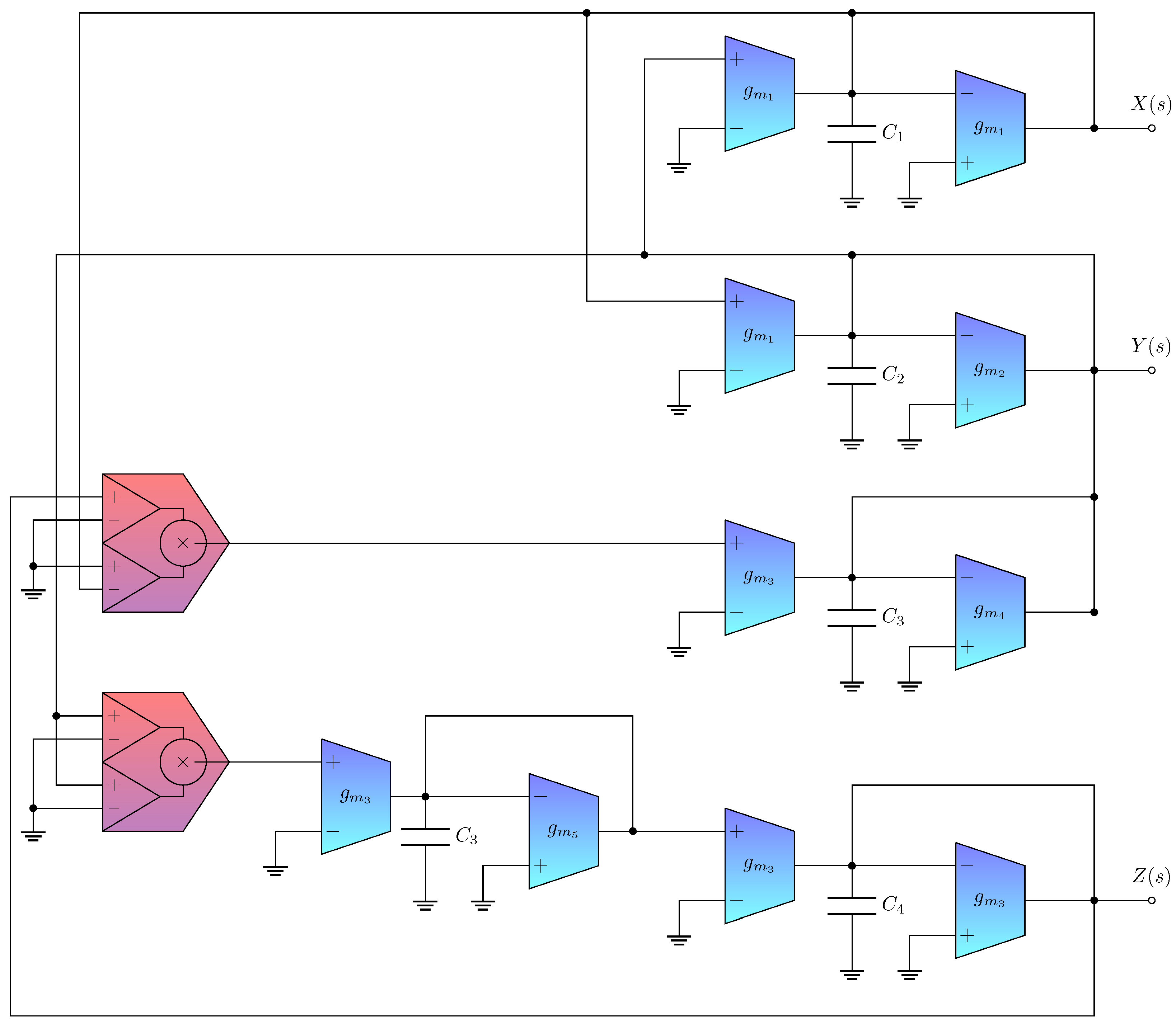
Equations (9), (10), and (12) can be simulated as the block description shown in Figure 9, which shows the labels of the three state variables and the first- and second-order (biquadratic) transfer functions, which are designed with OTA-C filters herein.
As shown in Figure 9, the convolution operations can be performed using a multiplier circuit, which can be designed with CMOS technology, as already shown in the tutorial given in [17]. In the same manner, the transfer functions can be associated to active filters that can be designed with OTA-C topologies, as shown in the tutorial [28]. The integrator based on OTA-C is shown in Figure 10. In this case, the transconductance of the OTAs and capacitance values can be calculated from the transfer function in voltage mode given at the bottom of the figure.
The block diagram shown in Figure 9 can be macro-modeled using integrators, multipliers, and OTA-C active filter topologies to generate the design shown in Figure 11. It can be appreciated that Figure 9 embeds four transfer functions whose OTA-C topologies require the values of transconductances () and capacitances that must be suitable for CMOS design. Table 1 lists the values of the transconductances and capacitances associated to CMOS first- and second-order active filters.
4. Design of OTA-C Biquad Filters
To accomplish each of the macro-modeling specifications of the OTA-C topologies, it is necessary to design five different transconductance () values. These must be suitable for the four active OTA-C filters listed in Table 1. For instance, the first of the OTAs will have the schematic structure shown in Figure 12, which is taken from [32], in order to achieve S. After sizing the MOSFETs, the width (W) and length (L) of the channel of each transistor and the resistor value are listed in Table 2.
For the case of obtaining , , and , one can use a variant of the OTA shown in Figure 12. Briefly, the updated topology includes source degeneration using resistors, as detailed in [33] and shown in Figure 13, where , which can be varied to tune the desired value. Some authors just vary the current bias, as shown in [34]; however, the transconductance may become nonlinear, so the best solution herein is the use of source degeneration topologies.
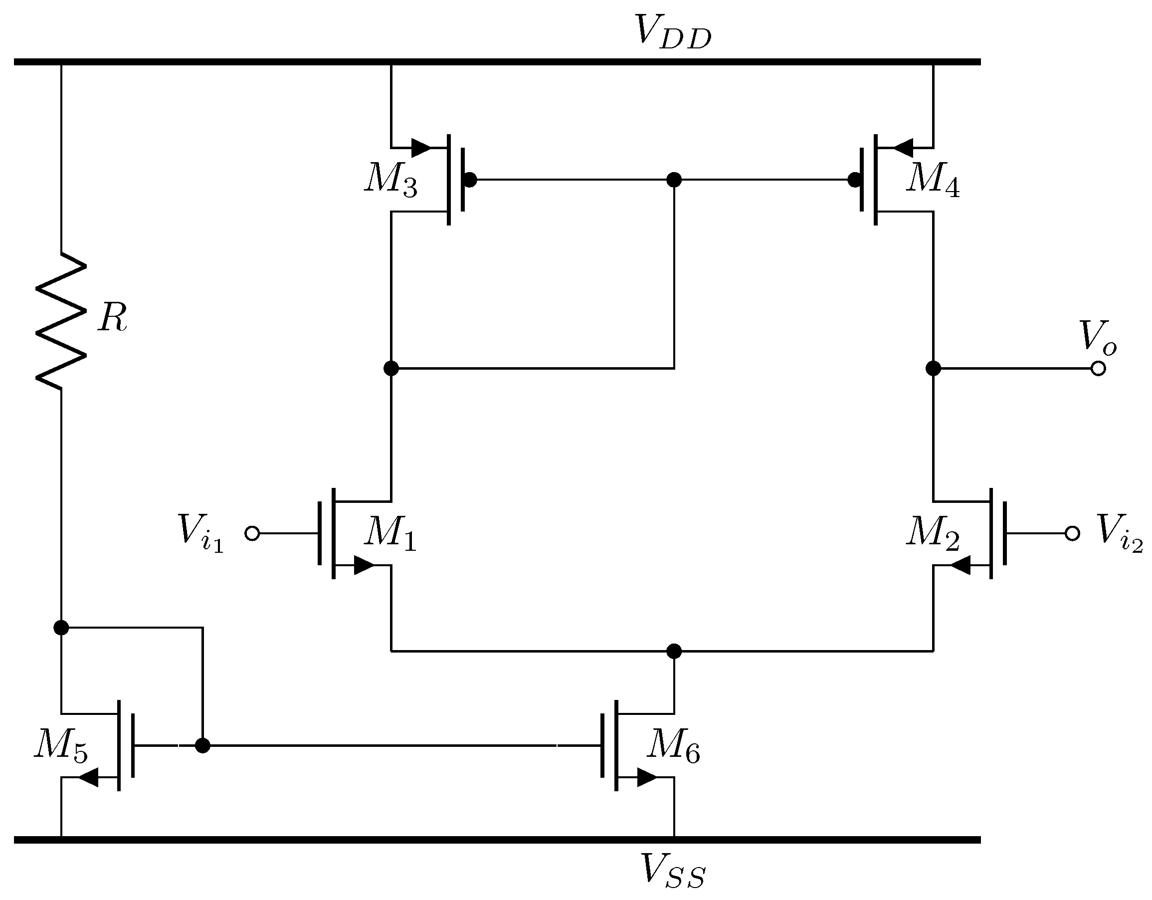
Finally, for the implementation of the OTA whose transconductance value should be = 500 S, the two-stage Miller topology shown in Figure 14, which is taken from [32], is implemented with its respective compensation stage composed of and . Table 3 shows the W/L dimensions of each MOSFET, as well as the passive circuit element values.
The direct CMOS design from Figure 11 mitigates chaotic behavior due to the fact that the biquadratic filter requires finding the right place for the poles, which is established as follows: The mathematical description of a second-order or biquadratic filter that satisfies (12) is given in (13).
where is the relative damping factor and is the undamped natural frequency. In this manner, (12) can be re-ordered as given in (14).
where it can be seen that and , so that at the end, the damping factor can be described by (15).
The damping factor can be tuned to generate the desired behavior, which, in this case, is chaotic behavior. Therefore, the damping factor depends on the values of and , as shown in (15), so depending on the value of , a system behaves as follows:
If , the system is overdamped.
If , the system is critically damped.
If , the system is underdamped.
If , the system is not damped, and it tends to oscillate.
By setting , then the damping factor depends on , as given in (16).
and plotting this function can help to visualize how depends on the values assigned to . Thus, by plotting the function given in (16), as shown in Figure 15, one can appreciate how the system behaves for values . In addition, one can see that point A on the graph represents the value of . In order to guarantee that the CMOS design of Lorenz systems based on biquadratic filters remains oscillating with chaotic behavior, a value of is chosen in order to modify its behavior over time. As a result, the SPICE simulations of the CMOS and OTA-C-based Lorenz systems are shown in Figure 16 and Figure 17.
5. Chaotic Masking Using OTA-C Filters
As described above, chaotic masking based on two synchronized systems in a master–slave topology can be performed as shown in Figure 5, where it can be appreciated that state variable Y is used to mask a signal. First, the simulation results of synchronizing two CMOS Lorenz systems using the Pecora and Carroll technique are shown in Figure 18a for state variable Y, whose are lower than 300 mV, and in Figure 18b for state variable Z, whose amplitudes are lower than 800 mV. The synchronization results can also be appreciated by plotting both state variables of the master and slave systems. So, Figure 19a shows the synchronization result for state variables Y, and Figure 19b shows the synchronization result for state variables Z. A good related work on synchronizing a numerical solution in a computer with an analog circuit can be found in [35]; other authors show how to reconstruct a system from data estimating additional members in resulting equations [36]. In this work, the original equations are scaled to allow the amplitudes of the state variables to be within ±1; then, they are synthesized by OTA-C topologies. Figure 20 shows the synchronization errors of the CMOS designs for state variables Y and Z of the master and slave systems. In each case, the root mean squared errors (RMSEs) are = 67.94 and = 101.68 .
By designing two CMOS Lorenz systems with OTA-C topologies, as detailed in Section 4, a whole CMOS secure communication system is developed from Figure 11. The master and slave systems provide chaotic times series taken from their state variables and , respectively. In the case of the CMOS design proposed herein, the transmitted signal () is a sinusoidal one and is masked with to generate signal , i.e., the channel that encrypts the input signal. As the slave system is well synchronized with the master one, the original signal can be recovered by subtracting the chaotic time series, obtaining . Finally, as , . This can be appreciated in Figure 21, where , and . It can be seen that during the transient behavior, one can see a pretty small difference between and , but after about 0.6 s, the error is almost zero, indicating that the recovered signal is the same as the transmitted one, while the encrypted one is masked in the chaotic time series.
6. Conclusions
We here show the design of Lorenz systems using OTA-C active filters implemented with 180 nm CMOS integrated circuit technology. As a particular case, the CMOS design consists of implementing three first-order low-pass filters and one biquadratic filter, whose damping factor is tuned to guarantee chaotic behavior, so that coefficient in the original Lorenz system is updated from 8/3 to 15, as detailed in Section 4.
A secure communication system is simulated by using the original values of the Lorenz systems that are simulated in Simulink. Afterwards, the mathematical model is scaled to allow for CMOS design that requires the amplitudes of the state variables to be bounded between ±1 Volt. The chaotic masking achieved by using two Lorenz systems synchronized in a master–slave topology and designed with CMOS OTA-C blocks shows its appropriateness for real applications in secure communications that require low-voltage supply, instead of using embedded systems as field-programmable gate arrays, which require higher voltage levels and power supply.
Author Contributions
Conceptualization, E.T.-C.; methodology, A.D.-S. and E.T.-C.; software, E.J.-M. and F.A.d.A.-D.; validation, E.J.-M. and F.A.d.A.-D.; formal analysis, E.J.-M.; investigation, A.D.-S. and E.T.-C.; writing—original draft preparation, E.J.-M. and F.A.d.A.-D.; writing—review and editing, E.T.-C. All authors have read and agreed to the published version of the manuscript.
Funding
This research received no external funding.
Data Availability Statement
Data is contained within the article.
Acknowledgments
Eduardo Juarez-Mendoza and Francisco Asahel del Angel-Diaz want to thank CONAHCyT-Mexico for the scholarships to pursue a master of science degree at Instituto Nacional de Astrofisica, Optica y Electronica (INAOE). Esteban Tlelo-Cuautle thanks CONAHCyT/Mexico for the support for sabbatical leave at CINVESTAV-Mexico through the program Apoyos complementarios para estancias sabaticas vinculadas a la consolidacion de grupos de investigacion 2023.
Conflicts of Interest
The authors declare no conflicts of interest.
References
- Lorenz, E.N. Deterministic nonperiodic flow. J. Atmos. Sci. 1963, 20, 130–141. [Google Scholar] [CrossRef]
- Zlatanovska, B.; Dimovski, D. Recurrent solutions of the Lorenz system of differential equations. Asian-Eur. J. Math. 2022, 15, 2250241. [Google Scholar] [CrossRef]
- Tse, C.; Lau, F. Chaos-based digital communication systems. In Operating Principles, Analysis Methods and Performance Evaluation; Springer: Berlin, Germany, 2003. [Google Scholar]
- Pecora, L.M.; Carroll, T.L. Synchronization of chaotic systems. Chaos 2015, 25, 097611. [Google Scholar] [CrossRef]
- Minati, L.; Innocenti, G.; Mijatovic, G.; Ito, H.; Frasca, M. Mechanisms of chaos generation in an atypical single-transistor oscillator. Chaos Solitons Fractals 2022, 157, 111878. [Google Scholar] [CrossRef]
- Sadia, M.; Paul, P.S.; Hasan, M.S. Compact Analog Chaotic Map Designs Using SOI Four-Gate Transistors. IEEE Access 2023, 11, 64782–64795. [Google Scholar] [CrossRef]
- Sadia, M.; Paul, P.S.; Hossain, M.R.; Muldrey, B.; Hasan, M.S. Robust Chaos With Novel 4-Transistor Maps. IEEE Trans. Circuits Syst.-Express Briefs 2023, 70, 914–918. [Google Scholar] [CrossRef]
- Jain, H.; Aggarwal, B.; Rai, S.K. New Modified Voltage Differencing Voltage Transconductance Amplifier (MVDVTA) based Meminductor Emulator and its Applications. Indian J. Pure Appl. Phys. 2023, 61, 239–246. [Google Scholar] [CrossRef]
- Aggarwal, B.; Rai, S.K.; Arora, A.; Siddiqui, A.; Das, R. A Floating Decremental/Incremental Meminductor Emulator Using Voltage Differencing Inverted Buffered Amplifier and Current Follower. J. Circuits Syst. Comput. 2023, 32, 2350243. [Google Scholar] [CrossRef]
- Bhardwaj, K.; Raj, N.; Srivastava, M. Electronically Tunable Circuit Realization of Multimemelement Function Simulator and Its Application to Chaos Generation. Int. J. Bifurc. Chaos 2023, 33, 2350030. [Google Scholar] [CrossRef]
- Bhardwaj, K.; Srivastava, M. Compact Charge-Controlled Memristance Simulator with Electronic/Resistive Tunability. J. Circuits Syst. Comput. 2022, 31, 2250094. [Google Scholar] [CrossRef]
- Shukla, G.; Paul, S.K. Electronically Tunable 3D Autonomous Chaotic Oscillator Employing Single CCCFA and Its Extension to 4D. IEEE Access 2022, 10, 108422–108439. [Google Scholar] [CrossRef]
- Ranjan, A.; Bhatt, V.; Singh, Y.S. Resistorless Chua’s diode implementation for chaotic oscillation employing single EXCCCII. AEU-Int. J. Electron. Commun. 2022, 156, 154398. [Google Scholar] [CrossRef]
- Choubey, C.K.; Paul, S.K. Systematic realisation of inductorless and resistorless Chua’s chaotic oscillator using VDGA. Int. J. Electron. 2023, 110, 1006–1027. [Google Scholar] [CrossRef]
- Minati, L.; Tokgoz, K.K.; Ito, H. Distributed sensing via the ensemble spectra of uncoupled electronic chaotic oscillators. Chaos Solitons Fractals 2022, 155, 111749. [Google Scholar] [CrossRef]
- Ouyang, Z.; Jin, J.; Yu, F.; Chen, L.; Ding, L. Fully Integrated Chen Chaotic Oscillation System. Discret. Dyn. Nat. Soc. 2022, 2022, 8613090. [Google Scholar] [CrossRef]
- Han, G.; Sanchez-Sinencio, E. CMOS transconductance multipliers: A tutorial. IEEE Trans. Circuits Syst.-Express Briefs 1998, 45, 1550–1563. [Google Scholar] [CrossRef]
- Ersoy, D.; Kacar, F. Electronically Charge-Controlled Tunable Meminductor Emulator Circuit With OTAs and Its Applications. IEEE Access 2023, 11, 53290–53300. [Google Scholar] [CrossRef]
- Aggarwal, B.; Rai, S.K.; Sinha, A. New memristor-less, resistor-less, two-OTA based grounded and floating meminductor emulators and their applications in chaotic oscillators. Integration 2023, 88, 173–184. [Google Scholar] [CrossRef]
- Rohilla, K.; Pushkar, K.L.; Kumar, R.; Raj, A. Resistorless First-Order Universal Filter Structures Employing OTAs with Independent Controllability of Gain and Pole Frequency. IETE J. Res. 2022, 1–21. [Google Scholar] [CrossRef]
- Wang, S.F.; Chen, H.P.; Ku, Y.; Lee, C.L. Versatile Voltage-Mode Biquadratic Filter and Quadrature Oscillator Using Four OTAs and Two Grounded Capacitors. Electronics 2020, 9, 1493. [Google Scholar] [CrossRef]
- Wang, S.F.; Chen, H.P.; Ku, Y.; Yang, C.M. Independently tunable voltage-mode OTA-C biquadratic filter with five inputs and three outputs and its fully-uncoupled quadrature sinusoidal oscillator application. AEU-Int. J. Electron. Commun. 2019, 110, 152822. [Google Scholar] [CrossRef]
- Peng, S.Y.; Lee, Y.H.; Wang, T.Y.; Huang, H.C.; Lai, M.R.; Lee, C.H.; Liu, L.H. A Power-Efficient Reconfigurable OTA-C Filter for Low-Frequency Biomedical Applications. IEEE Trans. Circuits Syst.-Regul. Pap. 2018, 65, 543–555. [Google Scholar] [CrossRef]
- Psychalinos, C.; Kasimis, C.; Khateb, F. Multiple-input single-output universal biquad filter using single output operational transconductance amplifiers. AEU-Int. J. Electron. Commun. 2018, 93, 360–367. [Google Scholar] [CrossRef]
- Bhanja, M.; Ray, B. Design of Configurable g(m)—C Biquadratic Filter. J. Circuits Syst. Comput. 2017, 26, 1750036. [Google Scholar] [CrossRef]
- Sotner, R.; Petrzela, J.; Jerabek, J.; Dostal, T. Reconnection-less OTA-based Biquad Filter with Electronically Reconfigurable Transfers. Elektron. Elektrotechnika 2015, 21, 33–37. [Google Scholar] [CrossRef]
- Prommee, P.; Pattanatadapong, T. Realization of Tunable Pole-Q Current-Mode OTA-C Universal Filter. Circuits Syst. Signal Process. 2010, 29, 913–924. [Google Scholar] [CrossRef]
- Sanchez-Sinencio, E.; Silva-Martinez, J. CMOS transconductance amplifiers, architectures and active filters: A tutorial. IEE Proc.-Circuits Devices Syst. 2000, 147, 3–12. [Google Scholar] [CrossRef]
- Shukla, G.; Paul, S.K. Smooth Nonlinearity Generation with lnCosh and Realization of Chaotic Oscillator. J. Circuits Syst. Comput. 2023, 32, 2350135. [Google Scholar] [CrossRef]
- Duan, Z.; Wang, H.; He, S.; Li, S.; Yan, S.; Zhao, X.; Yu, X.; Yang, G.; Tan, H. A fully integrated chaos generator based on voltage controlled oscillator. Microelectron. J. 2022, 126, 105514. [Google Scholar] [CrossRef]
- Joshi, M.; Ranjan, A. Low power chaotic oscillator employing CMOS. Integration 2022, 85, 57–62. [Google Scholar] [CrossRef]
- Razavi, B. Design of Analog CMOS Integrated Circuits, 2nd ed.; McGraw Hill: London, UK, 2017. [Google Scholar]
- Allen, P.E.; Dobkin, R.; Holberg, D.R. CMOS Analog Circuit Design; Elsevier: Amsterdam, The Netherlands, 2011. [Google Scholar]
- Aydin, Ş.Z.; Beken, G.N.; Taşkiran, Z.G.Ç. A Lorenz-like Chaotic OTA-C Circuit and Memristive Synchronization. Chaos Theory Appl. 2023, 5, 52–58. [Google Scholar] [CrossRef]
- Karimov, A.; Tutueva, A.; Karimov, T.; Druzhina, O.; Butusov, D. Adaptive generalized synchronization between circuit and computer implementations of the Rössler system. Appl. Sci. 2020, 11, 81. [Google Scholar] [CrossRef]
- Karimov, A.; Rybin, V.; Kopets, E.; Karimov, T.; Nepomuceno, E.; Butusov, D. Identifying empirical equations of chaotic circuit from data. Nonlinear Dyn. 2023, 111, 871–886. [Google Scholar] [CrossRef]
- Rybin, V.; Babkin, I.; Kvitko, D.; Karimov, T.; Nardo, L.; Nepomuceno, E.; Butusov, D. Estimating Optimal Synchronization Parameters for Coherent Chaotic Communication Systems in Noisy Conditions. Chaos Theory Appl. 2023, 5, 141–152. [Google Scholar] [CrossRef]
- Rybin, V.; Karimov, T.; Bayazitov, O.; Kvitko, D.; Babkin, I.; Shirnin, K.; Kolev, G.; Butusov, D. Prototyping the symmetry-based chaotic communication system using microcontroller unit. Appl. Sci. 2023, 13, 936. [Google Scholar] [CrossRef]
- Rybin, V.; Butusov, D.; Rodionova, E.; Karimov, T.; Ostrovskii, V.; Tutueva, A. Discovering chaos-based communications by recurrence quantification and quantified return map analyses. Int. J. Bifurc. Chaos 2022, 32, 2250136. [Google Scholar] [CrossRef]
Figure 1.
Implementation of the Lorenz oscillator in Matlab/Simulink from (2).
Figure 1.
Implementation of the Lorenz oscillator in Matlab/Simulink from (2).

Figure 2.
Time series of x, y, and z of the Lorenz system.

Figure 3.
Lorenz attractor in 3D space.

Figure 4.
Implementation of the synchronization technique in Matlab/Simulink.

Figure 5.
Chaotic masking by using two synchronized systems in a master–slave topology.

Figure 6.
Test signal given in (5), consisting of the sum of three sine signals of different frequency and equal amplitude.
Figure 6.
Test signal given in (5), consisting of the sum of three sine signals of different frequency and equal amplitude.

Figure 7.
Chaotic masking described by (6).
Figure 7.
Chaotic masking described by (6).

Figure 8.
Recovered signal described by (7).
Figure 8.
Recovered signal described by (7).


Figure 10.
Structure of an adjustable integrator OTA-C circuit in voltage-mode operation.

Figure 11.
Macro-modeling the block description shown in Figure 9 by using multipliers, integrators, and OTA-C active filter topologies.
Figure 11.
Macro-modeling the block description shown in Figure 9 by using multipliers, integrators, and OTA-C active filter topologies.

Figure 12.
Design of an OTA to obtain S.

Figure 13.
Source degeneration-based OTA design.

Figure 14.
Two-stage OTA to obtain = 500 S.

Figure 15.
Plot of given in (16) as a function of .
Figure 15.
Plot of given in (16) as a function of .

Figure 16.
Time series of Lorenz system designed with 180 nm CMOS integrated circuit technology from the OTA-C-based design shown in Figure 11.
Figure 16.
Time series of Lorenz system designed with 180 nm CMOS integrated circuit technology from the OTA-C-based design shown in Figure 11.

Figure 17.
Phase portraits of Lorenz system designed with OTA-C topologies, in which the damping factor of the biquadratic filter is tuned by setting .
Figure 17.
Phase portraits of Lorenz system designed with OTA-C topologies, in which the damping factor of the biquadratic filter is tuned by setting .

Figure 18.
Time-series results of two CMOS Lorenz systems designed with OTA-C active filters.

Figure 19.
Synchronization results of two CMOS Lorenz systems designed with OTA-C active filters.

Figure 20.
Errors of the synchronization of two CMOS Lorenz systems designed with OTA-C active filters.
Figure 20.
Errors of the synchronization of two CMOS Lorenz systems designed with OTA-C active filters.

Figure 21.
Chaotic masking of a sinusoidal signal with chaotic time series by using the scheme shown in Figure 5 and designing the whole system with 180 nm CMOS integrated circuit technology.
Figure 21.
Chaotic masking of a sinusoidal signal with chaotic time series by using the scheme shown in Figure 5 and designing the whole system with 180 nm CMOS integrated circuit technology.


Table 1.
Transconductance () and capacitance values to accomplish each transfer function shown in Figure 9, which are designed with OTA-C topologies as shown in Figure 11.
| Active Filter | [] | Capacitance [pF] |
|---|---|---|
| = 164.44 | = 16.44 | |
| , | = 5.87 | |
| , | = 1.25 | |
| , | = 50 |
Table 2.
W/L values of each MOSFET for the OTA shown in Figure 12, in order to obtain S.
Table 2.
W/L values of each MOSFET for the OTA shown in Figure 12, in order to obtain S.
| MOSFET | W/L Dimensions [] | Value [k] |
|---|---|---|
| - | ||
| - | ||
| - | ||
| R | - | 75 |
Table 3.
W/L dimensions of the MOSFETs and circuit element values of the two-stage OTA shown in Figure 14.
Table 3.
W/L dimensions of the MOSFETs and circuit element values of the two-stage OTA shown in Figure 14.
| MOSFET | W/L [m] | k | pF |
|---|---|---|---|
| - | - | ||
| - | - | ||
| - | - | ||
| - | - | ||
| - | 1.25 | - | |
| R | - | 20 | - |
| - | - | 0.5 |
Disclaimer/Publisher’s Note: The statements, opinions and data contained in all publications are solely those of the individual author(s) and contributor(s) and not of MDPI and/or the editor(s). MDPI and/or the editor(s) disclaim responsibility for any injury to people or property resulting from any ideas, methods, instructions or products referred to in the content. |
© 2024 by the authors. Licensee MDPI, Basel, Switzerland. This article is an open access article distributed under the terms and conditions of the Creative Commons Attribution (CC BY) license (https://creativecommons.org/licenses/by/4.0/).
Share and Cite
MDPI and ACS Style
Juarez-Mendoza, E.; del Angel-Diaz, F.A.; Diaz-Sanchez, A.; Tlelo-Cuautle, E. CMOS Design of Chaotic Systems Using Biquadratic OTA-C Filters. J. Low Power Electron. Appl. 2024, 14, 14. https://doi.org/10.3390/jlpea14010014
AMA Style
Juarez-Mendoza E, del Angel-Diaz FA, Diaz-Sanchez A, Tlelo-Cuautle E. CMOS Design of Chaotic Systems Using Biquadratic OTA-C Filters. Journal of Low Power Electronics and Applications. 2024; 14(1):14. https://doi.org/10.3390/jlpea14010014
Chicago/Turabian StyleJuarez-Mendoza, Eduardo, Francisco Asahel del Angel-Diaz, Alejandro Diaz-Sanchez, and Esteban Tlelo-Cuautle. 2024. "CMOS Design of Chaotic Systems Using Biquadratic OTA-C Filters" Journal of Low Power Electronics and Applications 14, no. 1: 14. https://doi.org/10.3390/jlpea14010014
Note that from the first issue of 2016, this journal uses article numbers instead of page numbers. See further details here.