
LC Tank Oscillator Based on New Negative Resistor in FDSOI Technology

Abstract
:1. Introduction
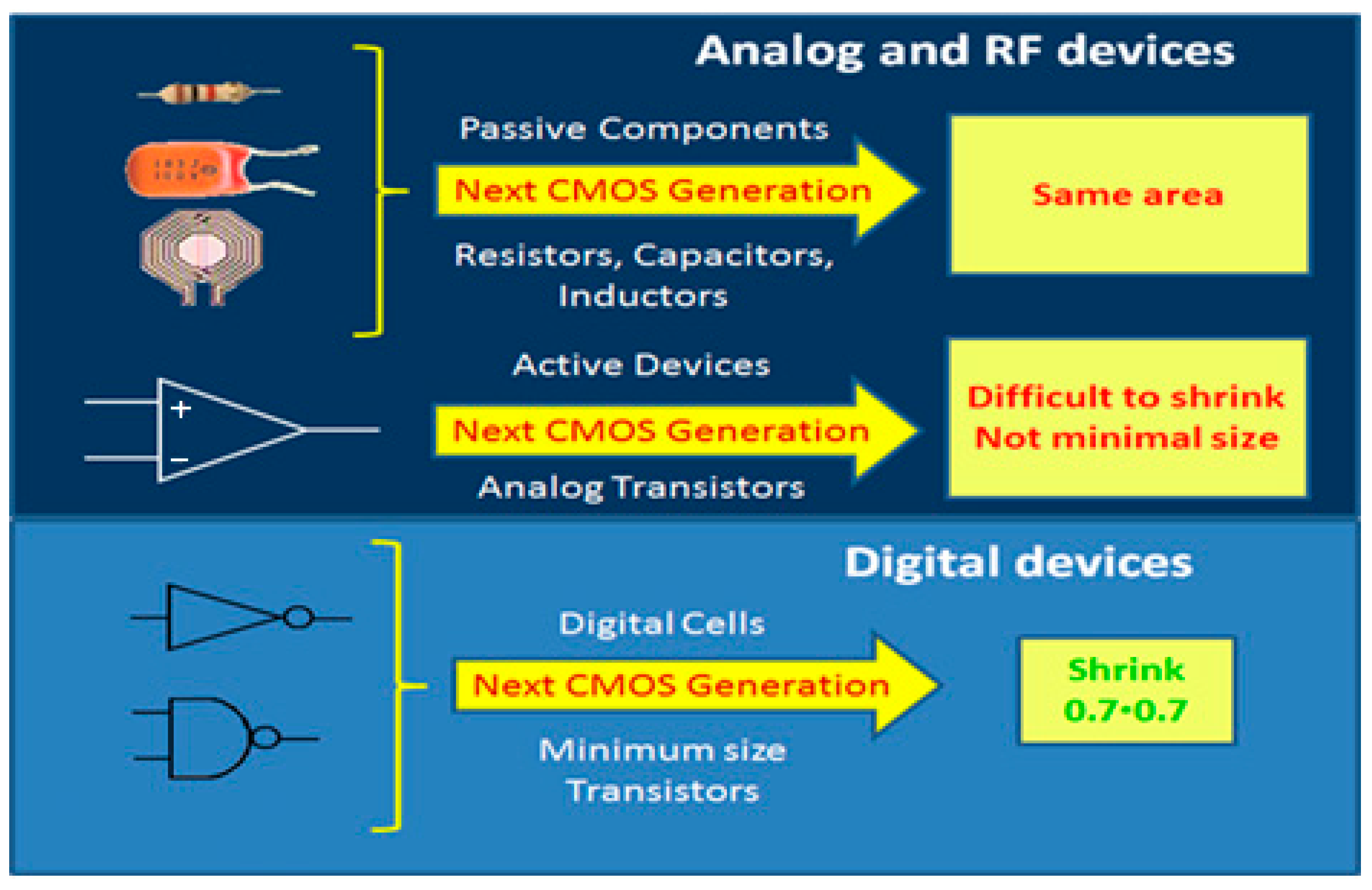
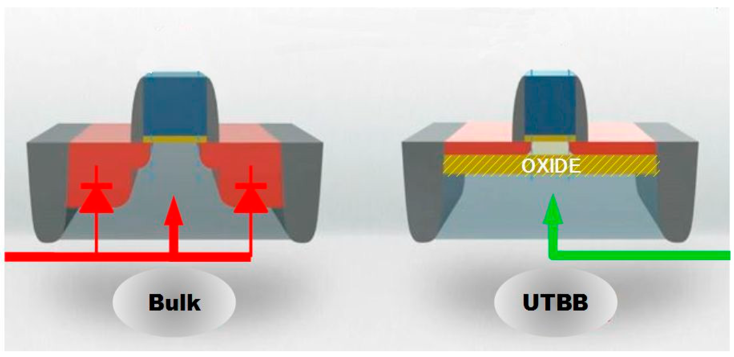
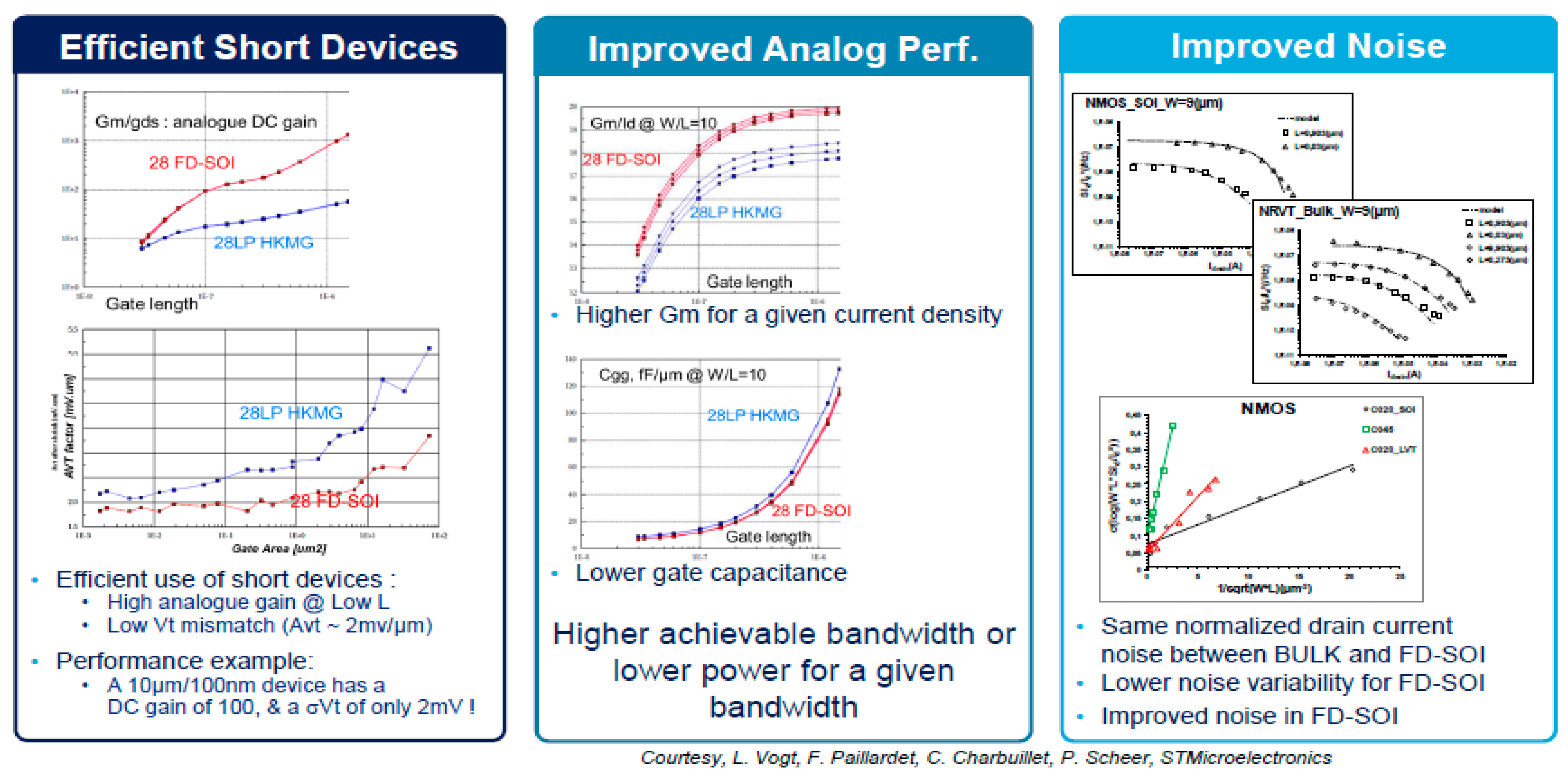
2. FDSOI Technology
3. Current Mirror
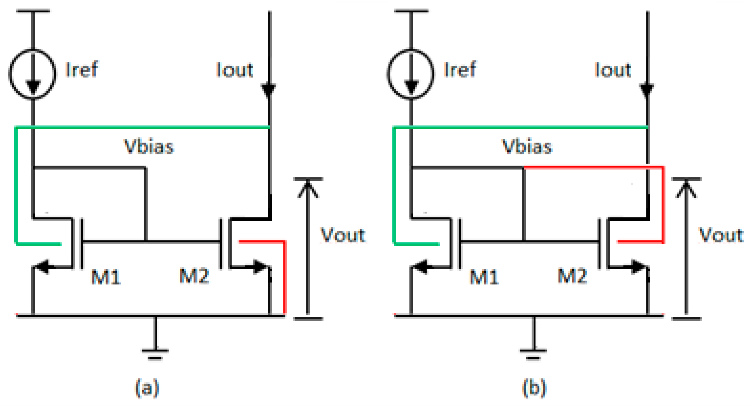
3.1. Classical Design
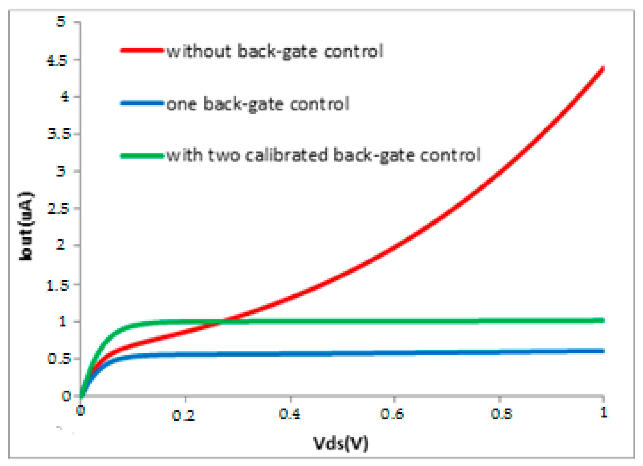
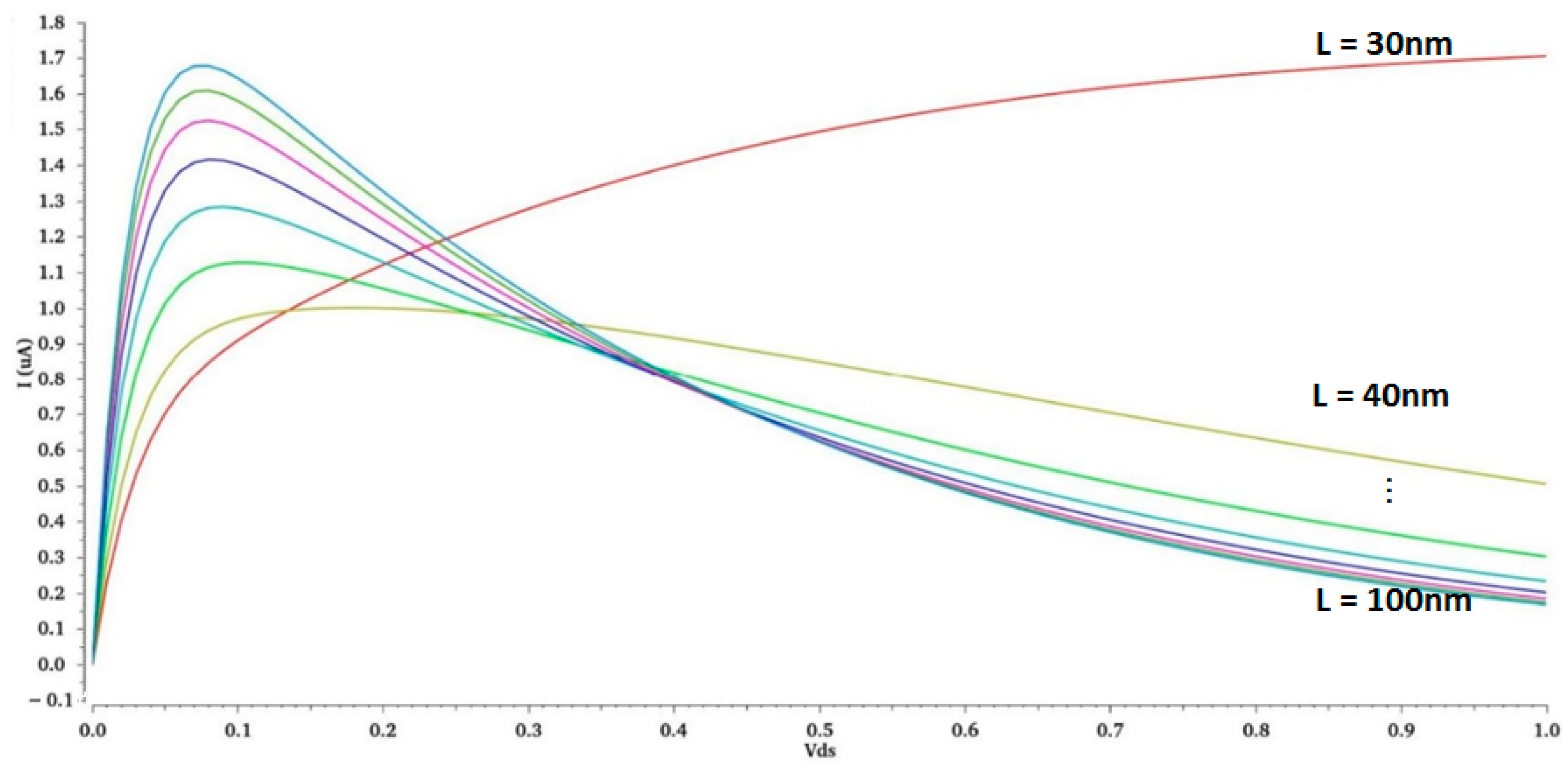
3.2. New Mirror Current Topology Using FDSOI Technology
3.3. Implementation and Measurements
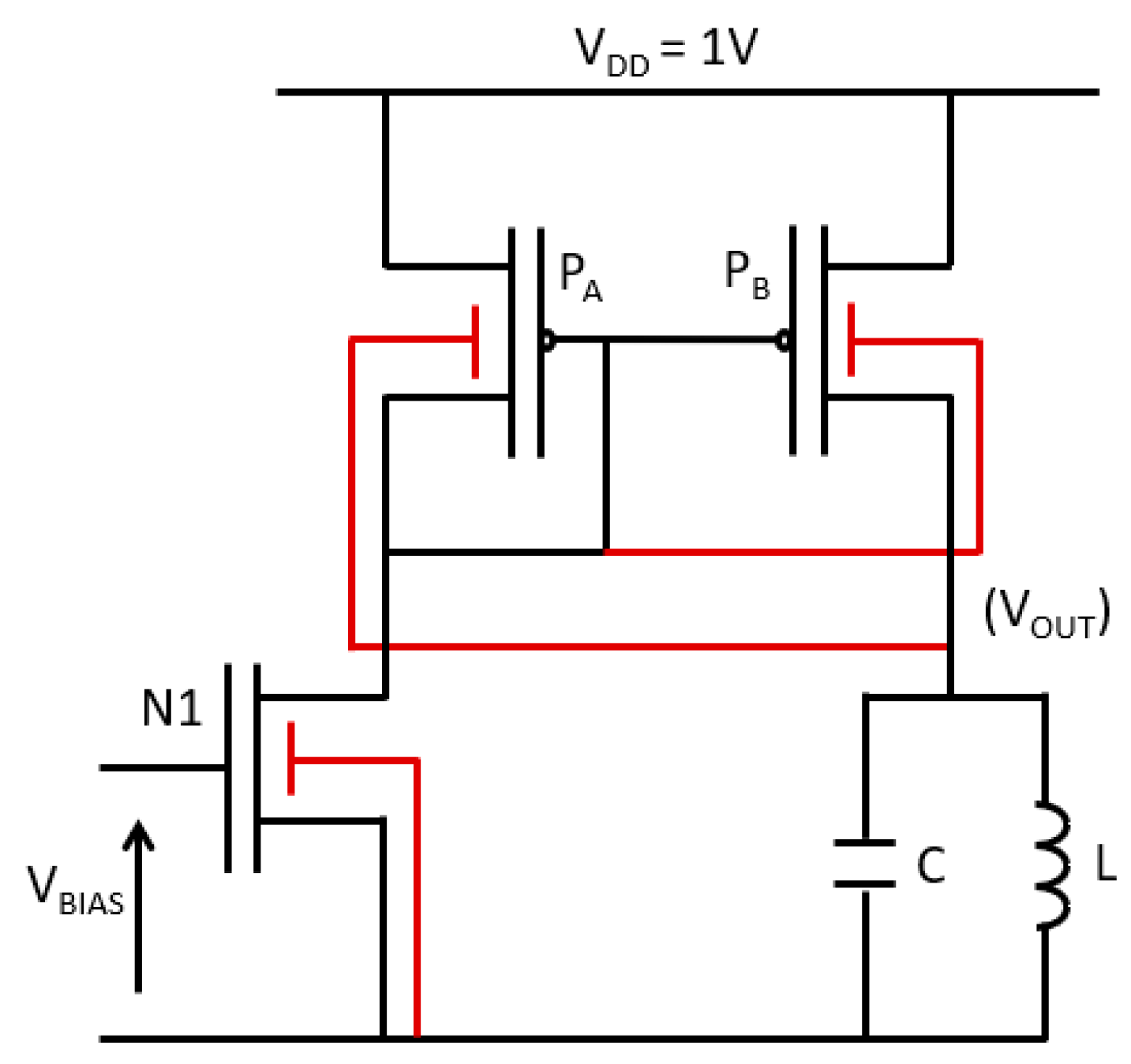
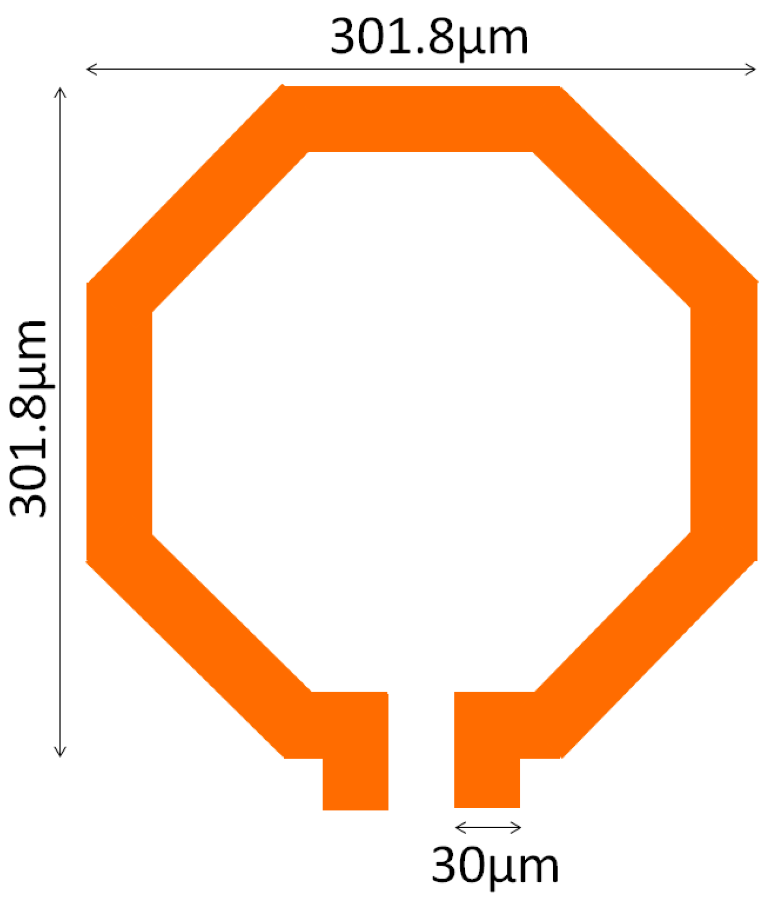
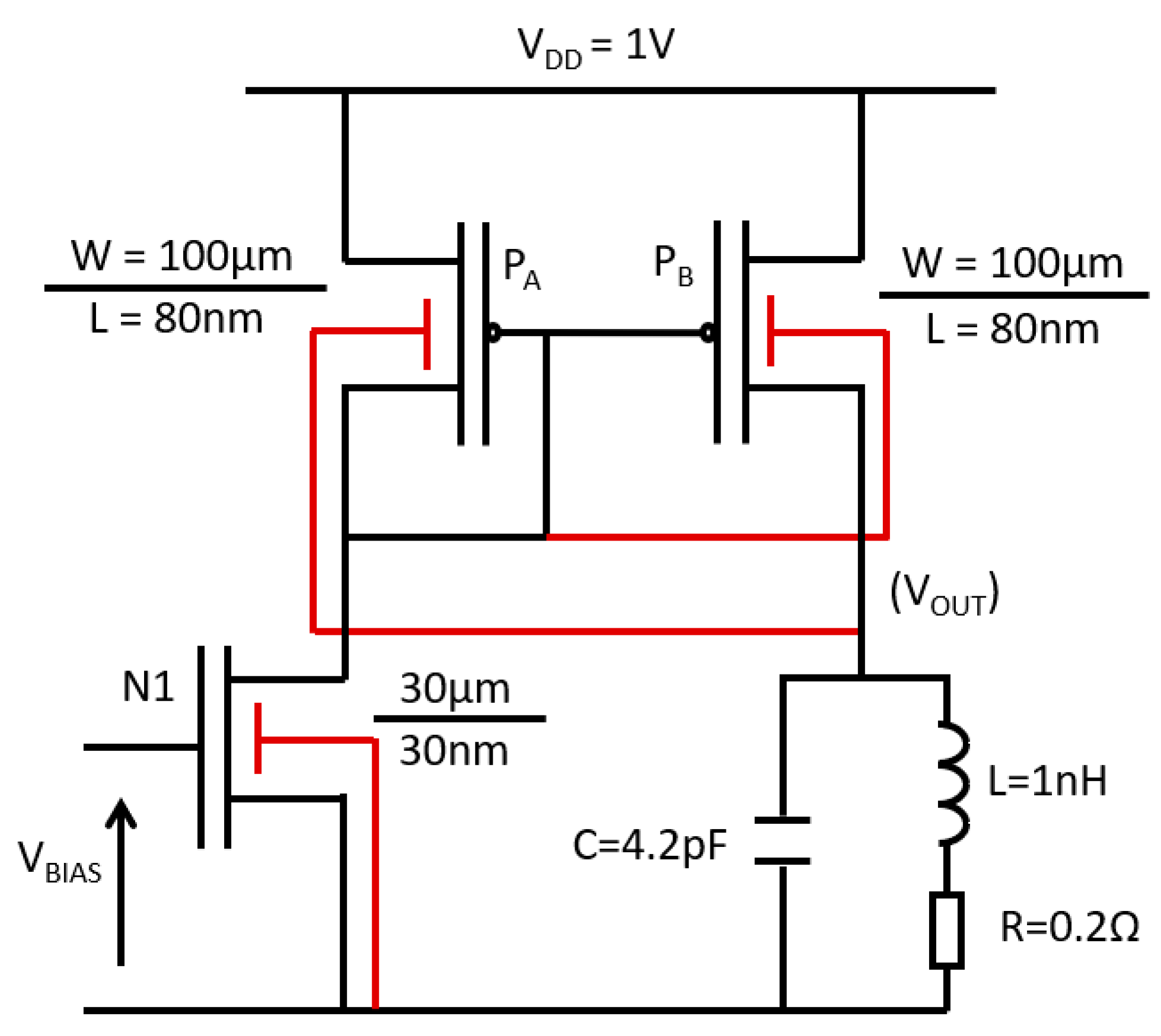
4. New LC Tank Oscillator
5. Comparison with Classical LC Tank VCO
6. Conclusions
Author Contributions
Funding
Data Availability Statement
Conflicts of Interest
References
- Samori, C.; Levantino, S.; Lacaita, A.L. Integrated LC oscillators for frequency synthesis in wireless applications. IEEE Commun. Mag. 2002, 40, 166–171. [Google Scholar] [CrossRef]
- Ham, D.; Hajimiri, A. Concepts and methods in optimization of integrated LC VCOs. IEEE J. Solid-State Circuits 2001, 36, 896–909. [Google Scholar] [CrossRef]
- Gurjar, R.; Mishra, D.K. Design and performance analysis of low phase noise LC-voltage controlled oscillator. TELKOMNIKA Telecommun. Comput. Electron. Control 2023, 21, 872–880. [Google Scholar] [CrossRef]
- Vosta, P.K.; Miar-Naimi, H.; Javadi, M. Comprehensive analysis of LC cross-coupled oscillator with active and passive transconductance amplification structure. Analog Integr. Circuits Signal Process. 2023, 115, 21–31. [Google Scholar] [CrossRef]
- Moore, G. Cramming more components onto integrated circuits. Electron. Mag. 1965, 38, 114. [Google Scholar] [CrossRef]
- Wei, Z.; Jacquemod, G.; Leduc, Y.; de Foucauld, E.; Prouvee, J.; Blampey, B. Reducing the short channel effect of transistors and reducing the size of analog circuits. Act. Passiv. Electron. Compon. 2019, 2019, 4578501. [Google Scholar] [CrossRef]
- Kumar, K.; Raman, A.; Raj, B.; Singh, S.; Kumar, N. Design and optimization of junctionless-based devices with noise reduction for ultra-high frequency applications. Appl. Phys. A 2020, 126, 913. [Google Scholar] [CrossRef]
- Mendiratta, N.; Tripathi, S.L. A review on performance comparison of advanced MOSFET structures below 45 nm technology node. J. Semicond. 2020, 41, 061401. [Google Scholar] [CrossRef]
- Verma, S.; Tripathi, S.L.; Bassi, M. Performance Analysis of FinFET device Using Qualitative Approach for Low-Power applications. In Devices for Integrated Circuit (DevIC), Kalyani, India; IEEE: Piscataway, NJ, USA, 2019; pp. 84–88. [Google Scholar] [CrossRef]
- Cathelin, A. Fully depleted silicon on insulator devices CMOS: The 28-nm node is the perfect technology for analog, RF, mmW, and mixed-signal system-on-chip integration. IEEE Solid-State Circuits Mag. 2017, 9, 18–26. [Google Scholar] [CrossRef]
- Cathelin, A. Advantages for Analog/RF & Mixed-Signal Designs; SOI Consortium Forum: Tokyo, Japan, 2016; Available online: https://www.semi.org/en/connect/events/fd-soi-and-rf-soi-forum-tokyo-japan-2016 (accessed on 26 November 2023).
- Pelgrom, M.J.M.; Duinmaijer, A.C.J.; Welbers, A.P.G. Matching properties of MOS transistors. IEEE J. Solid-State Circuits 1989, 24, 1433–1439. [Google Scholar] [CrossRef]
- Flatresse, P.; Wilson, R. SOC Variability Reduction: The UTBB FD-SOI Way; VARI: Darmstadt, Germany, 2013. [Google Scholar]
- Toumazou, C.; Lidgey, F.; Haigh, D. Analogue IC Design: The Current-Mode Approach; The Institution of Engineering and Technology: London, UK, 1993; p. 666. ISBN 978-0863412974. [Google Scholar]
- Wei, Z. Back-Gate Feedback for Auto-Calibration of Analog and Mixed Cells in UTBB-FDSOI Technology. Ph.D. Dissertation, Université Côte d’Azur, Côte d’Azur, France, 2019. [Google Scholar]
- Jacquemod, G.; Wei, Z.; Leduc, Y.; de Foucauld, E.; Prouvee, J. New design of analog and mixed-signal cells using back-gate cross-coupled structure. In Proceedings of the 2019 IFIP/IEEE 27th International Conference on Very Large Scale Integration (VLSI-SoC), Cuzco, Peru, 6–9 October 2019. [Google Scholar]
- Huq, S.M.I.; Baroi, O.L.; Shihab, S.A.; Biswas, S.N. Comparative Study and Design of Current Starved Ring Oscillators in 16 nm Technology. IEEE Trans. Circuits Syst. II Express Briefs 2021, 68, 1098–1102. [Google Scholar] [CrossRef]
- Afacan, E.; Dundar, G. A comprehensive analysis on differential cross-coupled CMOS LC oscillators via multi-objective optimization. Integration. VLSI J. 2019, 67, 162–169. [Google Scholar] [CrossRef]
- Hajimiri, A.; Lee, T.H. A general theory of Phase Noise in electrical oscillators. IEEE J. Solid-State Circuits 1998, 33, 174–194. [Google Scholar]
- Jafari, B.; Sheikhaei, S. Phase noise reduction in LC cross coupled oscillators using sinusoidal tail current shaping technique. Analog Integr. Circuits Signal Process. 2018, 96, 125–132. [Google Scholar] [CrossRef]
- Kassim, A.K.; Sharaf, K.; Ragaie, H. Tail current flicker noise reduction in LC VCOs by complementary switched biasing. In Proceedings of the IEEE 15th International Conference on Microelectronics, Cairo, Egypt, 11 December 2003; pp. 102–105. [Google Scholar]
- Jannesari, A.; Kamarei, M. Sinusoidal shaping of the ISF in LC oscillators. Int. J. Circuit Theory Appl. 2008, 36, 757–768. [Google Scholar] [CrossRef]
- Jafari, B.; Sheikhaei, S. Phase noise reduction in a CMOS LC cross coupled oscillator using a novel tail current noise second harmonic filtering technique. Microelectron. J. 2017, 65, 21–30. [Google Scholar] [CrossRef]
- Geynet, L.; de Foucauld, E.; Vincent, P.; Jacquemod, G. Fully integrated dual-band VCOs with power controlled by body voltage in 130nm CMOS/SOI for multi-standard applications. Analog Integr. Circuits Signal Process. 2007, 53, 43–51. [Google Scholar] [CrossRef]
- Dolt, D.; Livingston, Q.; Liu, T.; Kuma, A.; Palermo, S. SEE Sensitivity of a 16GHz LC-Tank VCO in a 22nm FinFET Technology. In Proceedings of the 2022 IEEE International Symposium on Circuits and Systems (ISCAS), Austin, TX, USA, 27 May 2022–1 June 2022; pp. 254–257. [Google Scholar] [CrossRef]
- Chen, Y.; Babaie, M.; Staszewski, R.B. A 350-mV 2.4-GHz quadrature oscillator with nearly instantaneous start-up using series LC tanks. In Proceedings of the IEEE Asian Solid-State Circuits Conference (A-SSCC), Seoul, Republic of Korea, 6–8 November 2017; IEEE: Piscataway, NJ, USA, 2017; pp. 104–108. [Google Scholar] [CrossRef]
- Hao, B.; Wang, Z.; Zhang, J.; Ma, M.; Wang, Y. A Low-Noise High-Robust LC-VCO Based on 22nm FD-SOI Process. In Proceedings of the 7th International Conference on Integrated Circuits and Microsystems (ICICM), Xi’an, China, 28–31 October 2022; IEEE: Piscataway, NJ, USA, 2022; pp. 166–170. [Google Scholar] [CrossRef]
- Jacquemod, G.; Benabedljelil, F.; Tatinian, W.; Lucchi, P.; Borgarino, M.; Carpineto, L. Comparison between RTW VCO and LC QVCO 12GHz PLLs. Analog Integr. Circuits Signal Process. 2012, 73, 749–756. [Google Scholar] [CrossRef]
- Monda, D.; Ciapri, G.; Mangraviti, G.; Berti, L.; Saporanara, S. Analysis and comparison of Ring and LC tank oscillators for 65nm integration of Rad-Hard VCO for SpaceFibre applications. In Applications in Electronics Pervading Industry, Environment and Society; Springer: Berlin/Heidelberg, Germany, 2019; pp. 25–32. [Google Scholar]
- Dolt, D.; Kim, I.; Palermo, S. A comparison of 25-GHZ-LC-VCO circuit topologies for SEU mitigation in 22nm FinFET. In Proceedings of the IEEE/MTT-S International Microwave Symposium, San Diego, CA, USA, 11–16 June 2023; pp. 151–154. [Google Scholar]


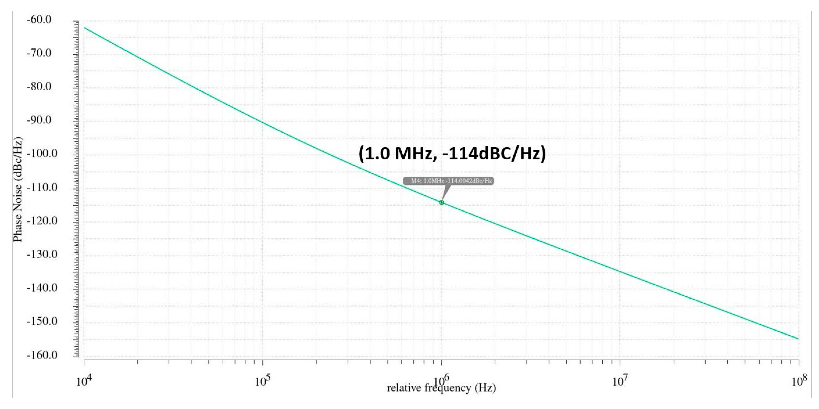
| VBIAS (V) | IREF (mA) | Settling Time (ns) | fosc (GHz) | PN (dBc/Hz @1 MHz) |
|---|---|---|---|---|
| 0.1–0.4 | No oscillation | |||
| 0.5 | 2.3 | 80 | 2.38 | −113 |
| 0.6 | 5.0 | 45 | 2.37 | −114 |
| 0.7 | 7.4 | 30 | 2.36 | −112 |
| 0.8 | 8.8 | 26 | 2.36 | −111 |
| 0.9 | 9.6 | 25 | 2.36 | −111 |
| 1.0 | 10.1 | 25 | 2.36 | −111 |
| Reference | [25] | [26] | [27] | This Work |
|---|---|---|---|---|
| Technology (nm) | 22 FinFET | 28 BULK | 22 FDSOI | 28 FDSOI |
| Supply Voltage (V) | 0.85 | 0.35 | 0.8 | 1 |
| fosc (GHz) | 16 | 2.4 | 24 | 2.4 |
| PN@1 MHz (dBc/Hz) | −98 | −110 | −93 | −114 |
| Power Dissipation (mW) | 5.94 | 1.3 | 20 | 9.26 |
| FOM (dB) | 174 | 176 | 168 | 172 |
| Simulation or measurement results | Measurement | Measurement | Simulation | Simulation |
Disclaimer/Publisher’s Note: The statements, opinions and data contained in all publications are solely those of the individual author(s) and contributor(s) and not of MDPI and/or the editor(s). MDPI and/or the editor(s) disclaim responsibility for any injury to people or property resulting from any ideas, methods, instructions or products referred to in the content. |
© 2024 by the authors. Licensee MDPI, Basel, Switzerland. This article is an open access article distributed under the terms and conditions of the Creative Commons Attribution (CC BY) license (https://creativecommons.org/licenses/by/4.0/).
Share and Cite
Mao, Y.; Charlon, Y.; Leduc, Y.; Jacquemod, G. LC Tank Oscillator Based on New Negative Resistor in FDSOI Technology. J. Low Power Electron. Appl. 2024, 14, 8. https://doi.org/10.3390/jlpea14010008
Mao Y, Charlon Y, Leduc Y, Jacquemod G. LC Tank Oscillator Based on New Negative Resistor in FDSOI Technology. Journal of Low Power Electronics and Applications. 2024; 14(1):8. https://doi.org/10.3390/jlpea14010008
Chicago/Turabian StyleMao, Yuqing, Yoann Charlon, Yves Leduc, and Gilles Jacquemod. 2024. "LC Tank Oscillator Based on New Negative Resistor in FDSOI Technology" Journal of Low Power Electronics and Applications 14, no. 1: 8. https://doi.org/10.3390/jlpea14010008