Article

Reliability Enhancement Methods for Relaxation Oscillator with Delay Time Cancellation

by
Kunpeng Xu
1,2,
Hongguang Dai
2,
Zhanxia Wu
2,
Zhibo Huang
3,
Guoqiang Zhang
4,*,
Xiaopeng Yu
1,
Wechang Wang
5 and
Gang Xuan
5
1
College of Integrated Circuits, Zhejiang University, Hangzhou 310000, China
2
Beijing Smartchip Microelectronics Technology Co., Ltd., Beijing 100000, China
3
College of Information Science & Electronic Engineering, Zhejiang University, Hangzhou 310000, China
4
School of Information Science and Engineering, NingboTech University, Ningbo 315100, China
5
Zexin Intelligent Technology Co., Ltd., Ningbo 315100, China
*
Author to whom correspondence should be addressed.
J. Low Power Electron. Appl. 2024, 14(4), 47; https://doi.org/10.3390/jlpea14040047
Submission received: 1 September 2024 / Revised: 23 September 2024 / Accepted: 23 September 2024 / Published: 26 September 2024

Abstract

:
Relaxation oscillators are preferred in low-frequency applications due to their lower power consumption and superior temperature stability. However, frequency errors arise from variations in the comparator’s offset voltage and delay time due to PVT changes. To address these issues, this paper proposes the low-power delay time cancellation (DTC) technique and several enhancement methods, including a novel offset trimming approach, an error state detection and recovery (ESDAR) circuit, and a specialized frequency-trimming method. Simulation results for an 8 MHz relaxation oscillator in a 40 nm CMOS process show that the proposed DTC technique and enhancements improve frequency variation due to power supply fluctuations to ±0.05% and reduce temperature-induced frequency variation to ±0.4%.

1. Introduction

Relaxation oscillators exhibit lower power consumption than LC oscillators, which typically operate at several GHz [1] and offer better temperature stability than ring oscillators [2] in low-frequency applications. Additionally, they are more cost-effective than quartz crystal oscillators due to their compatibility with CMOS technology. Consequently, they are extensively utilized in microcontroller units (MCUs) as sleep timers [3], systems’ main clock sources [4], and other applications [5]. However, a significant challenge affecting relaxation oscillators’ frequency errors is the variation in the comparator’s offset voltage and delay time due to changes in process, supply voltage, and temperature (PVT). These factors are the primary reasons why relaxation oscillators typically operate at frequencies below 1 MHz [6,7,8]. Temperature compensation for comparator delay is achieved using current sources with positive and negative temperature coefficients [9]. However, variations in comparator delay due to supply voltage remain an issue. Inverter-based comparators with trip point regulation can reduce comparator delay variations, but the results are limited by the resolution of trip point regulation [6,8]. The chopping technique is used to mitigate the comparator’s offset voltage [7]. However, delay time remains a significant factor affecting frequency error. The comparator delay cancellation effectively mitigates the impact of comparator delay and offset voltage, but it compromises current efficiency due to the use of four comparators [10]. Frequency locked loops (FLLs) can address these issues due to their high open-loop gain. For instance, integrating a standard relaxation oscillator within a voltage averaging feedback loop has successfully produced a 14 MHz oscillator with minimal temperature-induced frequency errors [11]. Similarly, incorporating a relaxation oscillator in a self-threshold-tracking loop has resulted in an 8 MHz low-power, and high-precision oscillator [12]. By utilizing FLL and a parallel combination of two switched resistors, the oscillator in [13] operates at 32 MHz with low frequency errors. Furthermore, the introduction of FLL and second-order temperature compensation significantly improved the oscillator’s frequency stability in [14]. However, oscillators with FLL often suffer from slow start-up time due to limited bandwidth. Therefore, it remains essential to mitigate the effects of the variations in the comparator’s offset voltage and delay time without using FLLs.
The primary contributions of this paper are twofold: first, we propose a low-power delay time cancellation (DTC) technique to address the aforementioned issues without relying on FLLs; second, we introduce a series of enhancement methods, including offset trimming, an error state detection and recovery (ESDAR) circuit, and a frequency-trimming method based on ESDAR, to improve the reliability of the relaxation oscillator. The organization of this paper is as follows: in Section 2, we explain how the comparator’s offset voltage and delay time affect the frequency of relaxation oscillators and introduce the principle of DTC. In Section 3, we analyze the tolerance limit of the DTC technique and propose an offset trimming method to enhance this tolerance. Section 4 provides a detailed description of the ESDAR circuit. In Section 5, we introduce a frequency-trimming method based on the ESDAR circuit. Section 6 presents the simulation results, and Section 7 offers a brief conclusion.

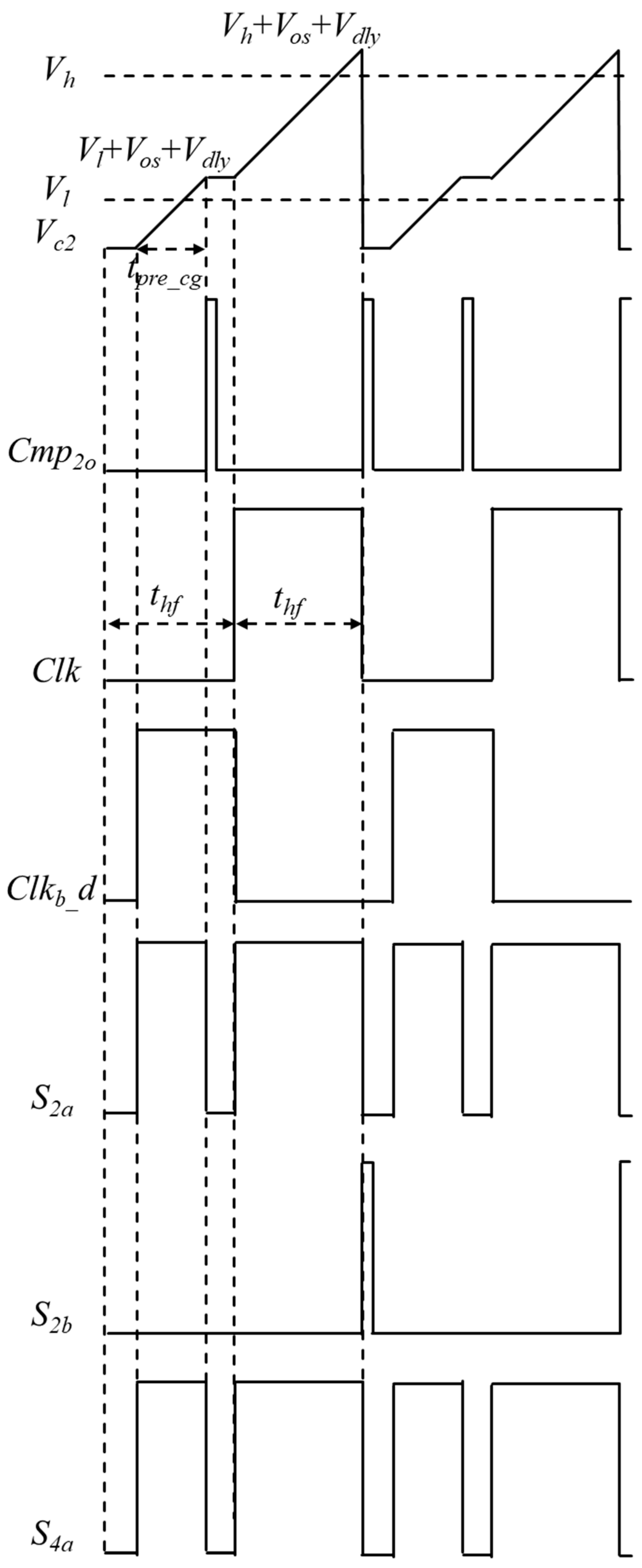
2. Principle of Delay Time Cancellation

The frequency of conventional relaxation oscillators is influenced by the comparators’ offset voltage (Vos) and delay time (td). As illustrated in Figure 1a, considering the impact of Vos and td, the comparator switches its state when Vin reaches Vl + Vos + Vdly (where Vl is the reference voltage) resulting in a period error of tos + td. If the reference voltage is increased to a higher level Vh, and Vin continues to rise from Vl + Vos + Vdly, the comparator will invert its state again when Vin reaches Vh + Vos + Vdly, as shown in Figure 1b. Then, the charge time t4 can be expressed as
t 4 = ( V h V l ) k ,
where k represents the slope of Vin. Equation (1) indicates that t4 is not affected by Vos and td. Therefore, this property can be utilized to mitigate the effects of Vos and td in the design of relaxation oscillators.
The proposed oscillator is depicted in Figure 2. It consists of a reference voltage generator providing Vh and Vl, a charging circuit, two comparators, a control circuit generating the control signals S1a, S2a, S3a, S4a, S1b, S2b, and an ESDAR circuit producing the reset signals Rstn1, Rstn2 and Rstn3. The waveforms of the signals around CMP2 are shown (the signals around CMP1 are not depicted due to the symmetry of the oscillator) in Figure 3. The delayed clock signal Clkb_d is utilized to generate the control signals S2a, S4a, and S2b. The signals S2a and S2b control the charging and discharging of capacitor C2, respectively.
The signal S4a regulates the voltage of Vref, enabling it to switch between Vh and Vl. With these control signals, the signal Vc2, which exhibits two charging phases within one clock cycle, can be obtained. During the first charging phase, Vc2 is charged to Vl + Vos + Vdly. In the second charging phase, Vc2 is charged to Vh + Vos + Vdly. Consequently, the period of the clock is given by
T = 2 t h f = 2 C [ ( V h + V o s + V d l y ) ( V l + V o s + V d l y ) ] I = 2 C ( V h V l ) I = 2 R C .
It is evident from Equation (2) that the period/frequency of the clock is not influenced by Vos and td.

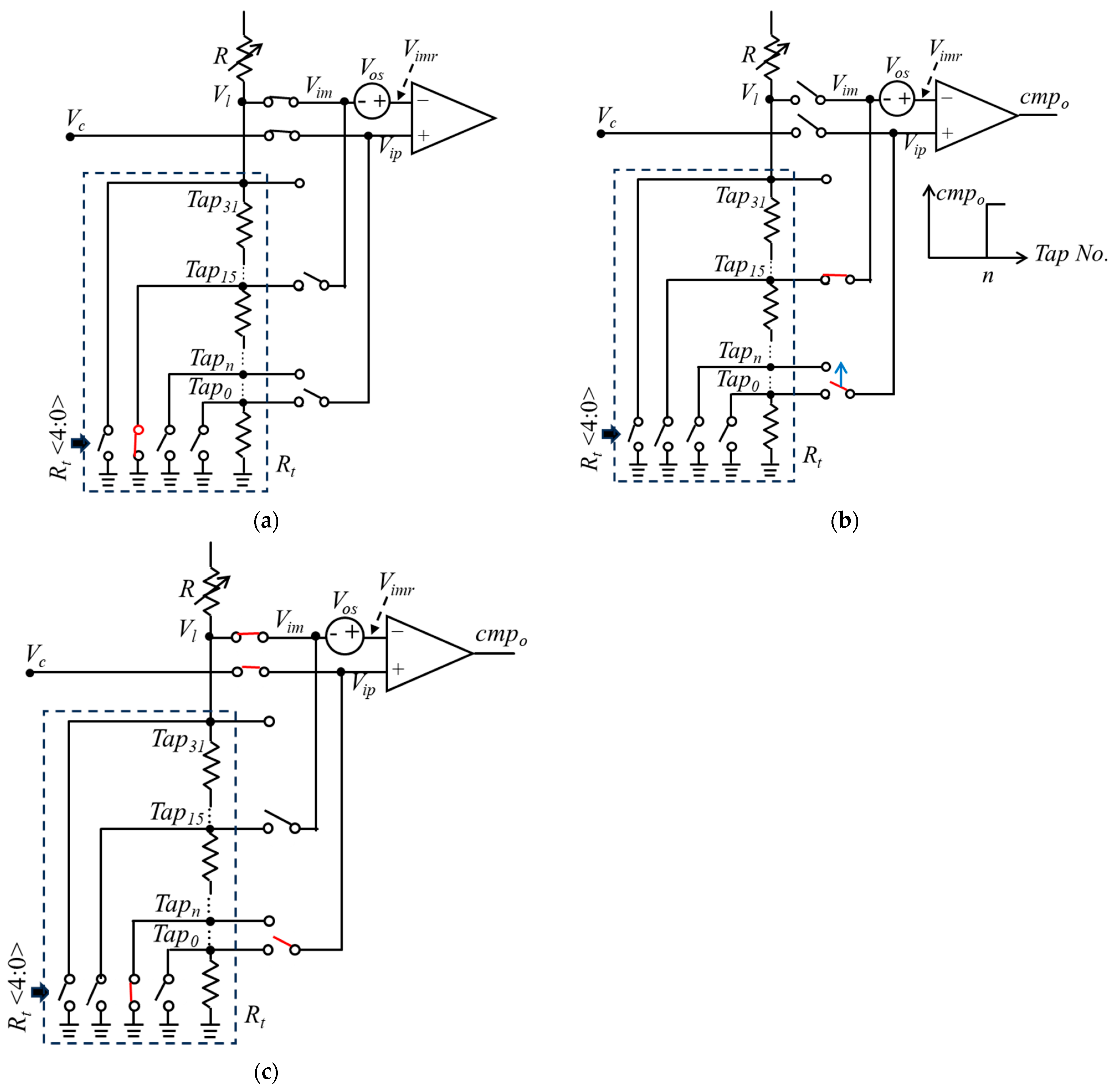
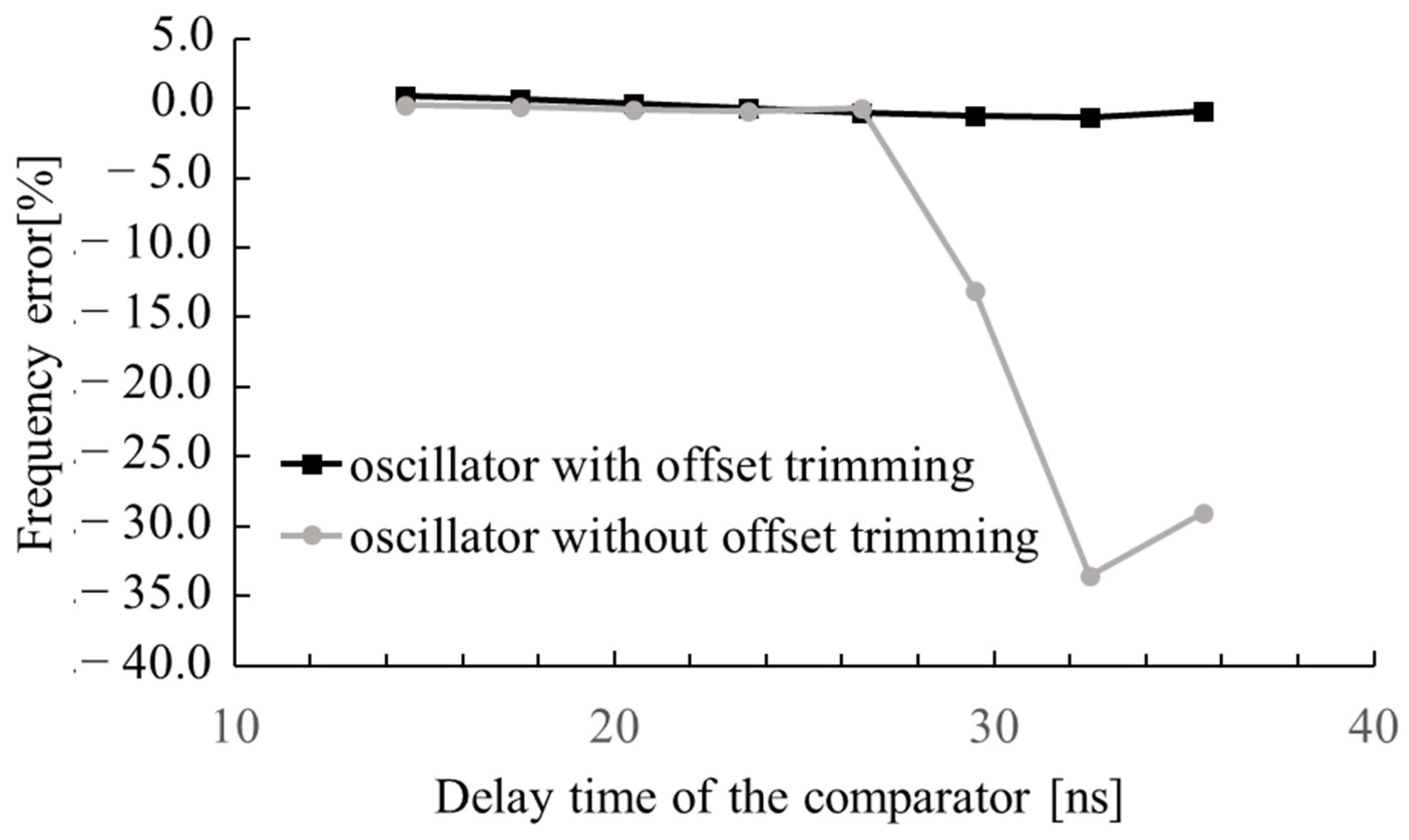
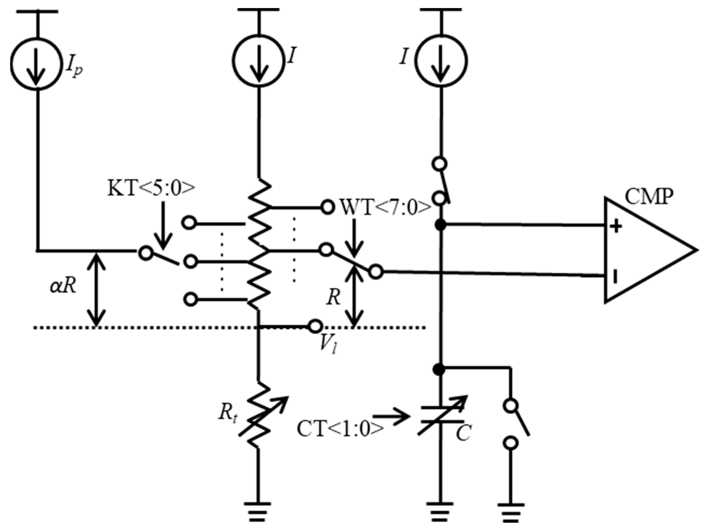
3. Tolerance Limit of the DTC Technique and Offset Trimming

Figure 3 illustrates that the time for the first charging phase, tpre_cg, must satisfy 0 < tpre_cg < thf. Consequently, we derive
0 < C V l + V o s + V d l y I < R C .
Given that
I = ( V h V l ) R ,
Equation (3) can be reformulated as
0 < V l + V o s + V d l y V h V l < 1 .
Thus, the range of Vos + Vdly can be expressed as
V l < V o s + V d l y < V h 2 V i .
Equation (6) illustrates that reducing Vos can decrease the comparator’s current draw, by allowing for a larger acceptable Vdly and td. Consequently, while reducing Vos does not reduce frequency error, it is beneficial for minimizing the oscillator’s power consumption. Thus, an offset trimming method is proposed to effectively reduce Vos.
To explain the offset trimming method, the relevant circuits, including the variable resistor R and Rt, and the comparator, are extracted from Figure 2 and redrawn as Figure 4, which includes the details of Rt. As depicted in Figure 4a, in the oscillator’s normal operation mode before offset trimming, the comparator’s input Vim is connected to Vl or Vh. The comparator’s input Vip is connected Vc. The 5-bit variable resistor Rt is set to its median value by grounding Tap15. Consequently, the voltage Vimr is given by
V i m r = V l 15 + V os
where Vl_15 denotes the voltage at Vl when Tap15 is connected to ground, serving as the reference voltage for offset trimming. Under these conditions, Vos reduces the acceptable maximum Vdly, as demonstrated in Equation (6).
Therefore, offset trimming should be performed before the oscillator enters its normal operation mode. The offset trimming process consists of two phases: the offset measurement phase and the resistance setting phase. In the offset measurement phase, all switches in Rt are deactivated via the control word Rt<4:0>. Tap15 is connected to Vim, and Vip iterates from Tap0 to Tap31 until the comparator’s output, cmpo, transitions to a high level. Assuming that cmpo transitions to a high level when Vip connects to Tapn, as illustrated in Figure 4b, the offset voltage Vos can be expressed as
V os = Δ V n 15
where ∆V represents the voltage drop across a unit resistor within Rt, and n denotes the Tap number that triggers a high-level output from the comparator. As deduced from Equation (8), the maximum offset trimming error is ∆V/2. The trimming range is defined as −15∆VVos ≤ 16∆V, ensuring a balanced range due to the selection of Vl_15 as the reference voltage for offset trimming.
Then during the resistance setting phase, as depicted in Figure 4c, Tapn is grounded. Consequently, the voltage Vimr is given by
V i m r   = V l 15 + ( 15 n ) Δ V + V o s = V l 15
It is shown that Vimr is not affected by Vos after offset trimming.
Given that the Vos of the comparator is specified to be 70 mV and the current flowing through Rt approximates 1.26 μA, the maximum Rt is deliberately set to 160 kΩ to achieve a trimming range of ±100 mV. Figure 5 depicts the oscillator’s tolerance to variations in the comparator’s delay time. Without offset trimming, a substantial frequency error arises when the delay time exceeds 26 ns. Conversely, with offset trimming, the tolerance limit extends to 36 ns. This demonstrates that the proposed offset trimming method effectively reduces the influence of Vos, thereby enhancing the oscillator’s tolerance to fluctuations in the comparator’s delay time. Therefore, a five-transistor amplifier with a 30 ns delay time is utilized in this work.

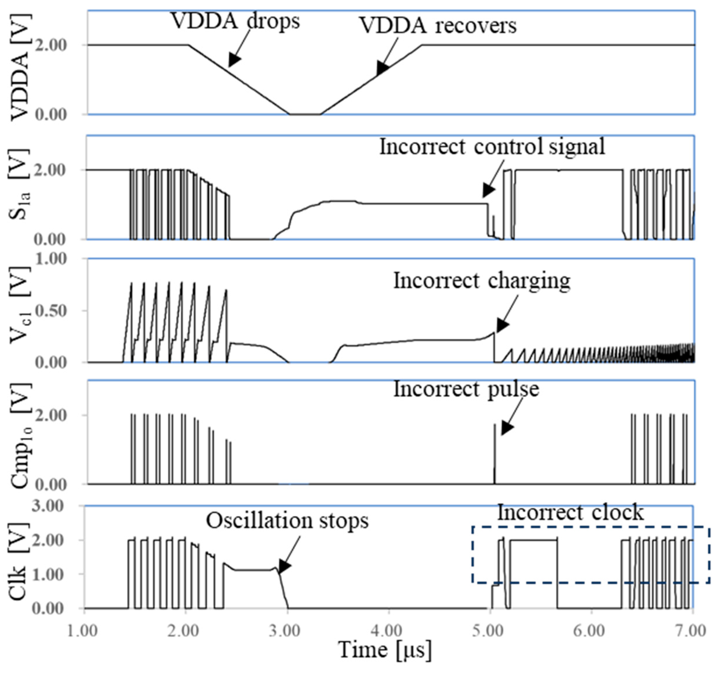
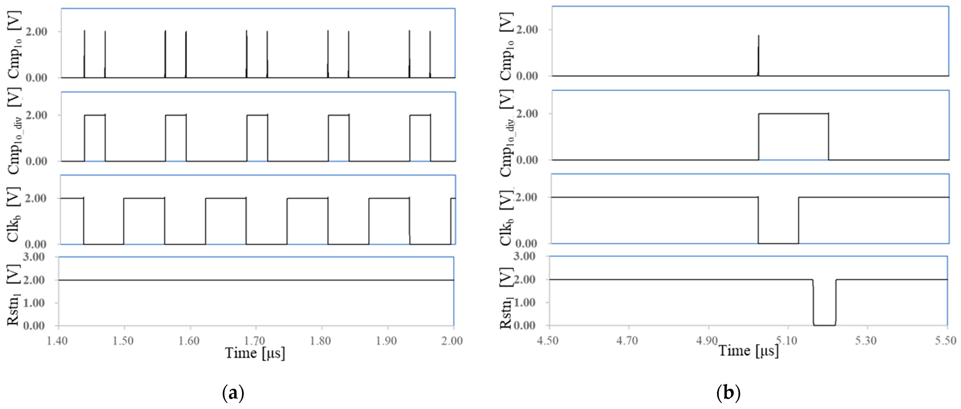
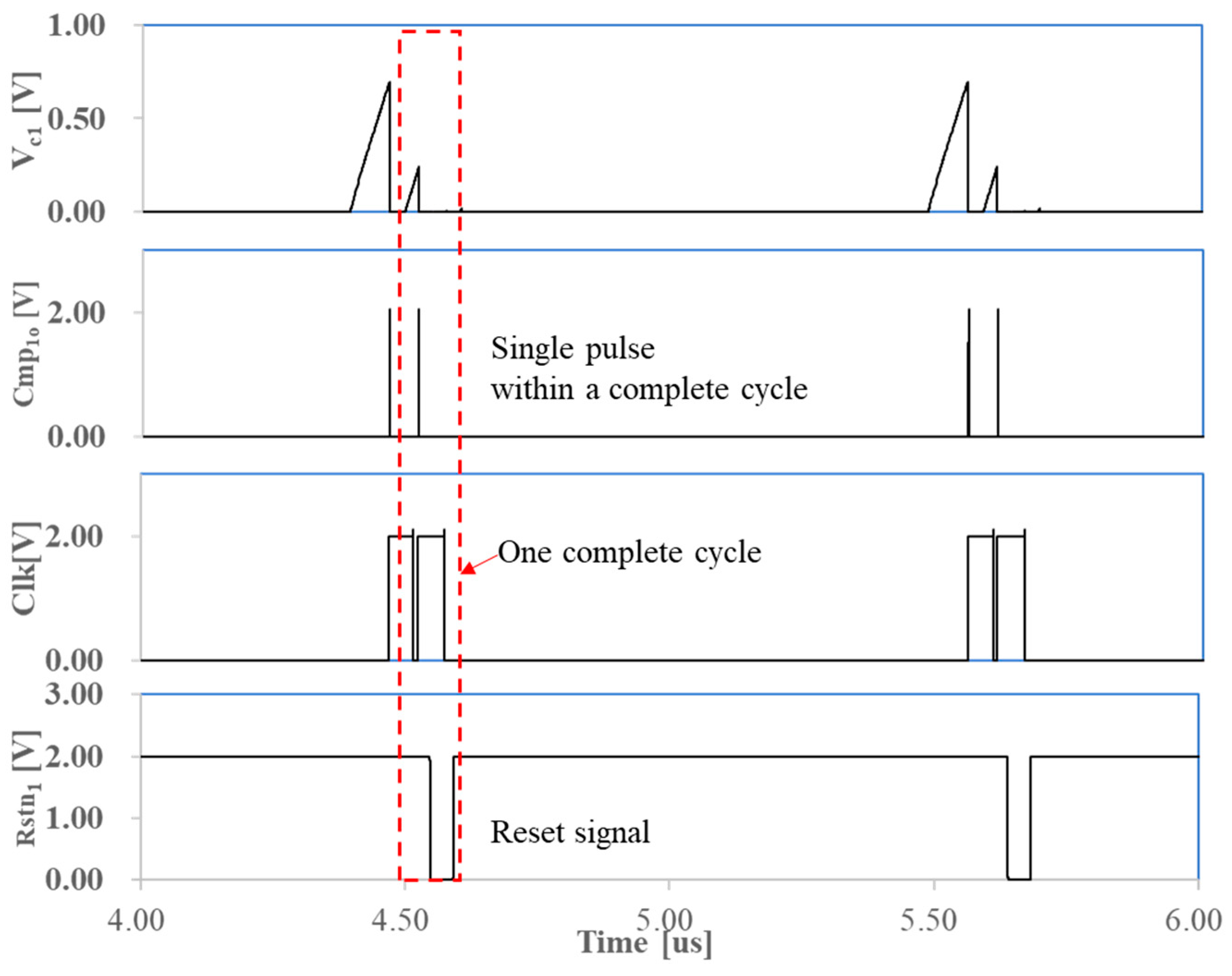
4. Error State Detection and Recovery Circuit

To enable the charging circuit to perform two distinct charging processes within a single cycle, as depicted in Figure 3, we propose a specialized control circuit, as illustrated in Figure 2. However, sudden changes in external conditions, such as a drop in supply voltage, may cause the control circuit to generate incorrect signals, leading to the incorrect clock signal shown in Figure 6. As depicted in Figure 6, the oscillation stops around 3 μs due to the drop in VDDA. Although VDDA recovers around 4.3 μs, the control circuit generates incorrect signals, including S1a, causing incorrect charging and output pulses from the comparators. This results in an undesired output clock from the oscillator.
To address this issue, we propose an ESDAR circuit, as illustrated in Figure 2. This circuit is capable of generating a reset signal in response to an incorrect output clock. It cannot be replaced by a power-on reset circuit because the conditions causing the incorrect output clock and those triggering the power-on reset circuit are not always the same. This circuit continuously monitors the outputs of the comparators and divides them using D-flip flops. One example of a divided signal, Comp1o_div, is shown in Figure 7a. When Comp1o_div is sampled by a D-flip flop synchronized with the Clkb clock signal, the output consistently remains high. Consequently, under normal operating conditions, the signal Rstn1 remains high, as depicted in Figure 7a.
In contrast, during abrupt changes in VDDA, the control circuit may generate erroneous signals, causing the comparator to produce only a single pulse within a complete cycle. Under such conditions, the output of the D-flip flop transitions to a low state, as illustrated in Figure 7b. Consequently, the signal Rstn1 also drops to a low state, initiating a reset of the oscillator. In the initial condition, the current mirrors in the RVG and CMP are disabled by Rstn1; the current mirrors in the charging circuit are disabled by Rstn2; and the signal Clk is held low by Rstn3, as shown in Figure 2.
Figure 8 depicts the operational response of the oscillator, incorporating the ESDAR circuit, to a sudden reduction in VDDA. At approximately 5.2 μs, the Rstn1 signal initiates the reset process of the oscillator, demonstrating the effectiveness of the ESDAR circuit. Simulation results indicate that the ESDAR circuit functions effectively within a VDDA drop slope range of 0.1 µs/V to 1 µs/V and a minimum voltage of 0 V to 1 V.

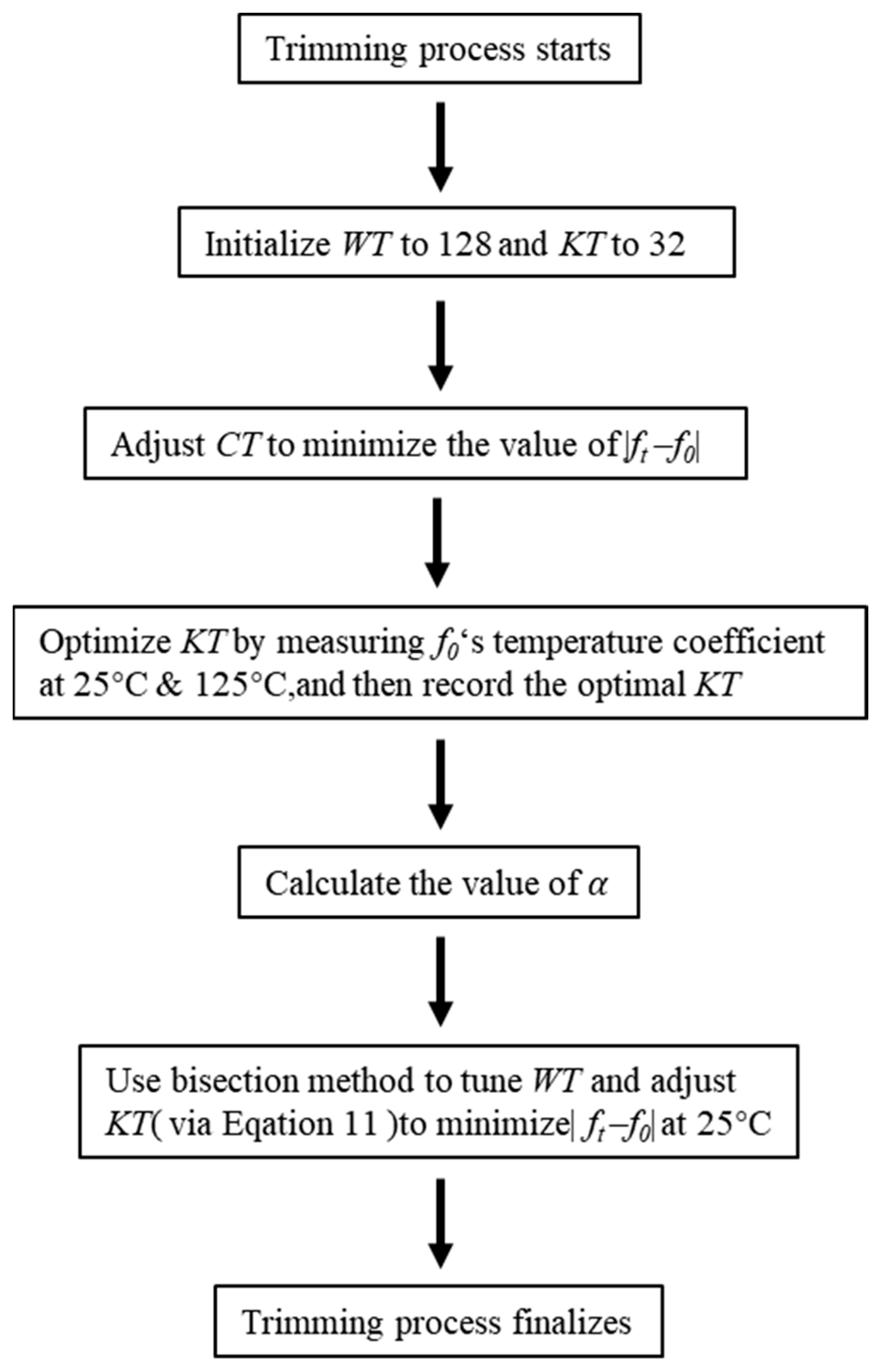
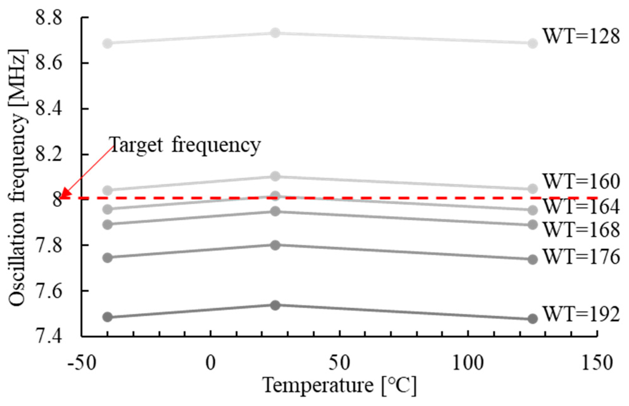
5. Frequency-Trimming Method

To mitigate frequency errors in relaxation oscillators, frequency trimming is essential. This process includes temperature compensation to compensate for the temperature-dependent variations in resistor R, and adjustment of the frequency variations caused by the process variation. The latter is achieved by modulating the variable resistor, R, and the variable capacitor, C, while temperature compensation is facilitated by introducing a positive temperature coefficient of absolute temperature (PTAT) current, Ip, into the circuit, as shown in Figure 9 [15]. As illustrated in Figure 9, the control word KT is used for temperature compensation. The control word WT is used to adjust the value of R by changing connections of the relevant switches. Considering the effect of Ip, the output clock frequency can be expressed as
f 0 = 1 2 R C I I + α I p ,
where α represents the position where Ip is inserted. If I is a zero-temperature coefficient current, the temperature coefficient of the current ratio I/(I + αIp) can be adjusted by modifying α, thereby compensating for the temperature-dependent variations in the resistor R.
However, as demonstrated in Equation (10) and Figure 9, f0 varies with changes in α, which in turn depends on alterations in resistance R. This implies that achieving the desired frequency requires a concurrent process of temperature compensation and adjustment of the absolute frequency value. Moreover, given the extensive combination possibilities of trim codes totaling 131,072 (stemming from an 8-bit WT code, a 6-bit KT code, a 2-bit CT code and two temperature points), the frequency measurement during the trimming process incurs significant costs. Therefore, optimizing this process is crucial for cost-effective and precise frequency control.
Fortunately, the relationship between the parameters α, KT and WT in this circuit can be expressed as
K T = ( B + W T ) α C A ,
where the constants A, B and C are set to 6, 280 and 88, respectively. By utilizing Equation (11), it becomes feasible to calculate the value of KT for any adjustment in WT, while keeping α constant. Consequently, the trimming process can be optimized using Equation (11). The proposed trimming flowchart is shown in Figure 10. Initially, WT and KT are set to 128 and 32, respectively. Next, CT is adjusted to make the current oscillation frequency f0 approach the target frequency ft. Subsequently, by measuring f0 at 25 °C and 125 °C with varying KT, the optimal KT that minimizes temperature-induced frequency error is determined, and the corresponding α is calculated. Then, WT is tuned using the bisection method, and KT is adjusted to maintain α constant until the frequency error |ftf0|at 25 °C is minimized. This concludes the frequency-trimming process.
Figure 11 illustrates the variations in f0 with respect to the change in WT, while keeping the optimal α. It demonstrates that the clock frequency can be adjusted without change the temperature efficient by using the proposed frequency-trimming process. With this process, the combination possibilities of trim codes can be reduced to 140, significantly reducing the frequency-trimming costs.
During the frequency-trimming process, the oscillation frequency may significantly exceed the target frequency, ft, such as in the condition of WT = 0, CT = 3. Under these circumstances, the oscillator may fail to function properly as it cannot meet the requirement of 0 < tpre_cg< thf, as mentioned in Section 3. To address this issue, the ESDAR circuit is introduced into the frequency-trimming process. As illustrated in Figure 12, when the oscillator malfunctions due to an excessively high frequency, the comparators produce only a single pulse within a complete cycle, resulting in a reset pulse from Rstn1. Therefore, the reset pulse indicates that the oscillation frequency is higher than target frequency during the frequency-trimming process.
The flowchart for using the bisection method to tune WT with the assistance of the ESDAR circuit is shown in Figure 13. First, initialize WT1 to 0 and WT2 to 255. Then, define WT3 as the integer value that most closely approximates the arithmetic mean of WT1 and WT2. Next, evaluate whether the following conditions are simultaneously satisfied, either both conditions 1 and 2, or conditions 1 and 3:
  • When WT is equal to WT3, the oscillation frequency is less than ft.
  • When WT is equal to WT1, the oscillation frequency is greater than ft.
  • When WT is equal to WT1, Rstn1 outputs a reset signal.
If these conditions are met concurrently, set the value of WT2 to be equal to WT3. If the conditions are not met concurrently, set the value of WT1 to be equal to WT3. This iterative procedure is continued until |WT1WT2| = 1. Ultimately, the final value of WT is selected as the one between WT1 and WT3 that results in the minimum frequency error. By following the procedures shown in Figure 10 and Figure 13, the frequency-trimming process can be implemented successfully.

6. Simulation Results

The proposed DTC technique and reliability enhancement methods are implemented in an 8 MHz relaxation oscillator designed using a 40 nm CMOS process. The oscillator’s duty cycle ranges from 48% to 51% across PVT variations. This duty cycle error is primarily caused by fluctuations in the driving capability of the RS flip-flop within the control circuit. Figure 14a demonstrates that with the DTC technique, the frequency variation due to power supply voltage fluctuations is improved to ±0.05%. Figure 14b illustrates that within the temperature range of −40 °C to 125 °C, the frequency variation is reduced to approximately ±0.4% (due to the second-order dependence of the resistor) with the DTC technique, compared to ±0.8% without it. The frequency variations at fast-fast (ff) and slow-slow (ss) corners are also illustrated in Figure 14, highlighting the stability of frequency despite process variations. The performance comparison with other open-loop relaxation oscillators is presented in Table 1. As shown, the oscillators operating below 1 MHz demonstrated improvements in both current efficiency and temperature-induced frequency variations. However, enhancing these performances for oscillators operating above 1 MHz remains challenging. The proposed DTC technique and reliability enhancement methods, however, enable the relaxation oscillator to operate at higher frequencies with low frequency variation and improved current efficiency.

7. Conclusions

This paper presents a series of enhancements to the DTC technique to improve the reliability of relaxation oscillators. The proposed offset trimming approach, ESDAR circuit, and specialized frequency-trimming method have shown significant improvements in frequency stability and tolerance to PVT variations. The simulation results demonstrate the effectiveness of the proposed methods in enabling relaxation oscillators to operate at higher frequencies with low frequency variation and reduced current consumption. The voltage overhead in the resistor Rt may limit its application in low voltage conditions, necessitating future improvements. To enhance the credibility of this research, we will implement layout design, timing verification, post-layout simulation, fabrication and measurement in our subsequent work.

Author Contributions

Conceptualization, K.X. and G.Z.; methodology, K.X.; software, K.X., H.D., Z.W. and Z.H.; validation, K.X., H.D., Z.W. and Z.H.; formal analysis, K.X.; investigation, K.X.; resources, G.Z.; data curation, K.X.; writing—original draft preparation, K.X.; writing—review and editing, K.X., H.D., Z.W., Z.H., G.Z., X.Y., W.W. and G.X.; visualization, K.X., H.D., Z.W. and Z.H.; supervision, G.Z. and X.Y.; project administration, G.Z.; funding acquisition, G.Z. All authors have read and agreed to the published version of the manuscript.

Funding

This research received no external funding.

Data Availability Statement

Data is contained within the article.

Conflicts of Interest

Kunpeng Xu, Hongguang Dai and Zhanxia Wu were employed by Beijing Smartchip Microelectronics Technology Co., Ltd. Wechang Wang and Gang Xuan were employed by Zexin Intelligent Technology Co., Ltd. The remaining authors declare that the research was conducted without any commercial or financial relationships that could be interpreted as a potential conflict of interest.

References

  1. Ichihashi, M.; Harada, S.; Kanaya, H. 3.3-mA 2.8-GHz bufferless LC oscillator directly driving a 10-mm on-chip clock distribution line. IEICE Electron. Express 2019, 16, 20190301. [Google Scholar] [CrossRef]
  2. Xu, Z.; Kawahara, T. A Saturating-Integrator-Based Behavioral Model of Ring Oscillator Facilitating PLL Design. IEICE Trans. Electron. 2017, E100C, 370–372. [Google Scholar] [CrossRef]
  3. Duran, C.; Wachs, M.; Huntington, A.; Ardila, J.; Kang, J.; Amaya, A.; Gomez, H.; Romer, J.; Fernandez, L.; Flechas, F.; et al. An Energy-Efficient RISC-V RV32IMAC Microcontroller for Periodical-Driven Sensing Applications. In Proceedings of the IEEE Custom Integrated Circuits Conference (CICC), Boston, MA, USA, 22–25 March 2020. [Google Scholar]
  4. Xia, J.; Chen, Z. A 36 MHz Relaxation Oscillator with ±0.2% Temperature Variation for MCU Application. In Proceedings of the IEEE 4th International Conference on Circuits and Systems (ICCS), Chengdu, China, 23–26 September 2022. [Google Scholar]
  5. Wang, T.; Griffith, D.; Ahmed, M.G.; Zhu, J.; Wei, D.; Elkholy, A.; Elmallah, A.; Hanumolu, P.K. A 6 μW ± 50 ppm/°C ± 1500 ppm/V 1.5 MHz RC Oscillator Using Self-Regulation. IEEE Trans. Circuits Syst. II Express Briefs 2019, 66, 1297–1301. [Google Scholar]
  6. Sun, J.; Han, Y.; Qian, Y. A low power low supply sensitivity current-mode relaxation oscillator. IEICE Electron. Express 2014, 11, 20140877. [Google Scholar] [CrossRef]
  7. Paidimarri, A.; Griffith, D.; Wang, A.; Burra, G.; Chandrakasan, A.P. An RC Oscillator with Comparator Offset Cancellation. IEEE J. Solid-State Circuits 2016, 51, 1866–1877. [Google Scholar] [CrossRef]
  8. Li, Z.; Li, Z.; Zhao, H.; Zhao, H.; Yin, J.; Yin, J.; Qiao, S.; Qiao, S.; Zhou, Y.; Zhou, Y. A fully integrated RC oscillator with adaptive-body-biasing. IEICE Electron. Express 2022, 19, 20220102. [Google Scholar] [CrossRef]
  9. Chiang, Y.-H.; Liu, S.-I. A Submicrowatt 1.1-MHz CMOS Relaxation Oscillator with Temperature Compensation. IEEE Trans. Circuits Syst. II Express Briefs 2013, 60, 837–841. [Google Scholar] [CrossRef]
  10. Mikulić, J.; Schatzberger, G.; Barić, A. A 1-MHz on-chip relaxation oscillator with comparator delay cancelation. In Proceedings of the 43rd IEEE European Solid State Circuits Conference, Leuven, Belgium, 11–14 September 2017. [Google Scholar]
  11. Tokunaga, Y.; Sakiyama, S.; Matsumoto, A.; Dosho, S. An on-chip CMOS relaxation oscillator with voltage averaging feedback. IEEE J. Solid-State Circuits 2010, 45, 1150–1158. [Google Scholar] [CrossRef]
  12. Lu, S.-Y.; Liao, Y.-T. A low-power, differential relaxation oscillator with the self-threshold-tracking and swing-boosting techniques in 0.18-μm CMOS. IEEE J. Solid-State Circuits 2019, 54, 392–402. [Google Scholar]
  13. Khashaba, A.; Zhu, J.; Ahmed, M.; Pal, N.; Hanumolu, P.K. A 34 µW 32 MHz RC oscillator with ±530 ppm inaccuracy from −40 °C to 85 °C and 80 ppm/V supply sensitivity enabled by pulse-density modulated resistors. In Proceedings of the IEEE International Solid-State Circuits Conference, San Francisco, CA, USA, 16–20 February 2020. [Google Scholar]
  14. Zhang, G.; Cao, L.; Yayama, K.; Katsushima, A.; Miki, T. A differential on chip oscillator with 1.47-μs startup time and 3.3-ppm/°C temperature coefficient of frequency. IEICE Trans. Fundam. Electron. Commun. Comput. Sci. 2021, E104.A, 499–505. [Google Scholar]
  15. Pan, S.; Cheng, Y.; Wu, G.; Wang, Z.; Makinwa, K.A.A.; Wu, H. 3.2 A 0.028 mm2 32 MHz RC Frequency Reference in 0.18 μm CMOS with ±900 ppm Inaccuracy from −40 °C to 125 °C and ±1600 ppm Inaccuracy after Accelerated Aging. In Proceedings of the IEEE International Solid-State Circuits Conference (ISSCC), San Francisco, CA, USA, 13 November 2024; pp. 56–58. [Google Scholar]
  16. Chiang, Y.-H.; Liu, S.-I. Nanopower CMOS Relaxation Oscillators With Sub-100 ppm/°C Temperature Coefficient. IEEE Trans. Circuits Syst. II Express Briefs 2014, 61, 661–665. [Google Scholar]
  17. Huang, K.-K.; Wentzloff, D.D. A 1.2-MHz 5.8-μW Temperature-Compensated Relaxation Oscillator in 130-nm CMOS. IEEE Trans. Circuits Syst. II Express Briefs 2014, 61, 334–338. [Google Scholar]
  18. Zhou, W.; Goh, W.L.; Gao, Y. A 3-MHz 17.3-μW 0.015% Period Jitter Relaxation Oscillator with Energy Efficient Swing Boosting. IEEE Trans. Circuits Syst. II Express Briefs 2020, 67, 1745–1749. [Google Scholar]
  19. Liu, Y.; Zhu, Z.; Bao, R.; Lin, J.; Yin, J.; Li, Q.; Mak, P.-I.; Yang, S. A Compact Sub-nW/kHz Relaxation Oscillator Using a Negative-Offset Comparator with Chopping and Piecewise Charge-Acceleration in 28-nm CMOS. IEEE Trans. Circuits Syst. I Regul. Pap. 2024, 71, 515–525. [Google Scholar] [CrossRef]
  20. Lei, K.-M.; Mak, P.-I.; Martins, R.P. A 0.35-V 5200-μm2 2.1-MHz Temperature-Resilient Relaxation Oscillator With 667 fJ/Cycle Energy Efficiency Using an Asymmetric Swing-Boosted RC Network and a Dual-Path Comparator. IEEE J. Solid-State Circuits 2021, 56, 2701–2710. [Google Scholar] [CrossRef]
  21. Tokairin, T.; Nose, K.; Takeda, K.; Noguchi, K.; Maeda, T.; Kawai, K.; Mizuno, M. A 280 nW, 100 kHz, 1-cycle start-up time, on-chip CMOS relaxation oscillator employing a feedforward period control scheme. In Proceedings of the 2012 Symposium on VLSI Circuits (VLSIC), Honolulu, HI, USA, 13–15 June 2012; pp. 16–17. [Google Scholar]
  22. Aiello, O.; Crovetti, P.; Alioto, M. A Sub-Leakage PW-Power HZ-Range Relaxation Oscillator Operating with 0.3 V–1.8 V Unregulated Supply. In Proceedings of the 2018 IEEE Symposium on VLSI Circuits, Honolulu, HI, USA, 18–22 June 2018; pp. 119–120. [Google Scholar]
  23. Jeong, S.; Lee, I.; Blaauw, D.; Sylvester, D. A 5.8 nW CMOS Wake-Up Timer for Ultra-Low-Power Wireless Applications. IEEE J. Solid-State Circuits 2015, 50, 1754–1763. [Google Scholar] [CrossRef]
  24. Wang, H.; Mercier, P.P. A Reference-Free Capacitive-Discharging Oscillator Architecture Consuming 44.4 pW/75.6 nW at 2.8 Hz/6.4 kHz. IEEE J. Solid-State Circuits 2016, 51, 1423–1435. [Google Scholar] [CrossRef]
  25. Nadeau, P.M.; Paidimarri, A.; Chandrakasan, A.P. Ultra Low-Energy Relaxation Oscillator With 230 fJ/cycle Efficiency. IEEE J. Solid-State Circuits 2016, 51, 789–799. [Google Scholar] [CrossRef]
  26. Lee, J.; George, A.K.; Je, M. An Ultra-Low-Noise Swing-Boosted Differential Relaxation Oscillator in 0.18-μm CMOS. IEEE J. Solid-State Circuits 2020, 55, 2489–2497. [Google Scholar] [CrossRef]
  27. Choe, K.; Bernal, O.D.; Nuttman, D.; Je, M. A precision relaxation oscillator with a self-clocked offset-cancellation scheme for implantable biomedical SoCs. In Proceedings of the 2009 IEEE International Solid-State Circuits Conference-Digest of Technical Papers, San Francisco, CA, USA, 8–12 February 2009; pp. 402–403,403a. [Google Scholar]
Figure 1. (a) Impact of Vos and delay time td on comparator response; (b) reduction in Vos and td impact using DTC technique.
Jlpea 14 00047 g001
Figure 2. Structure of the proposed oscillator.
Jlpea 14 00047 g002
Figure 3. Timing waveforms of the proposed relaxation oscillator.
Jlpea 14 00047 g003
Figure 4. Connections of the comparator and Rt (a) before the offset trimming; (b) during the offset measurement phase; (c) during the resistance setting phase.
Jlpea 14 00047 g004
Figure 5. Oscillator tolerance to comparator delay time variations with and without offset trimming.
Jlpea 14 00047 g005
Figure 6. Incorrect signals generated by control circuit resulting in incorrect clock when a sudden VDDA drop occurs without ESDAR circuit.
Jlpea 14 00047 g006
Figure 7. Operating mechanism of the ESDAR circuit: (a) under normal condition, (b) during abrupt changes in VDDA.
Jlpea 14 00047 g007
Figure 8. ESDAR circuit generating reset signals to restore correct oscillation following a sudden VDDA drop.
Jlpea 14 00047 g008
Figure 9. Structure of frequency-trimming circuit.
Jlpea 14 00047 g009
Figure 10. Proposed frequency-trimming process.
Jlpea 14 00047 g010
Figure 11. Variations in f0 with respect to the change in WT, while keeping optimal α.
Jlpea 14 00047 g011
Figure 12. Oscillator malfunctions due to an excessively high frequency.
Jlpea 14 00047 g012
Figure 13. Flowchart for using bisection method to tune WT with the assistant of the ESDAR circuit.
Jlpea 14 00047 g013
Figure 14. Frequency variation due to (a) power supply and (b) temperature fluctuations.
Jlpea 14 00047 g014
Table 1. Performance comparison with other open-loop relaxation oscillators.
[6][7][8][9][10][16]
Process [nm]1806555180350180
Freq. [Hz]100 k18.5 k33 k1.1 M1 M28 k
Current eff. [μA/MHz]5.479.240.463.61.19
Temp. sen. [ppm/°C]518558644895.5
Temp. range [°C]−40~85−40~90−40~125−20~80−40~125−20~80
Line sen. [%/V]0.450.7530.283
*2 FoM [μA·(108 MHz·°C·V)−1]110.62972.9403.383.3863.9340.9
Trimming points for temperature compensation------
Type of resultsSimulationMeasurementSimulationMeasurementMeasurementMeasurement
[17][18][19][20][21][22]
Process [nm]13065282890180
Freq. [Hz]1.2 M3 M28.5 k2.1 M100 k4
Current eff. [μA/MHz]4.835.771.211.853.52.08
Temp. sen. [ppm/°C]296133.333.3158104.640,000
Temp. range [°C]−40~800~90−40~85−20~120−40~90−20~40
Line sen. [%/V]3.60.61.926.89.3710
*2 FoM [μA·(108 MHz·°C·V)−1]5150.4461.376.87841.53431.4830,000
Trimming points for temperature compensation--13--
Type of resultsMeasurementMeasurementMeasurementMeasurementMeasurementMeasurement
[23][24][25][26][27]This Work
Process [nm]1806518018013040
Freq. [Hz]112.81810.5 M3.2 M8 M
Current eff. [μA/MHz]439.431.70.3914.958.483.6
Temp. sen. [ppm/°C]45126020,000137125348
*2 291
Temp. range [°C]−10~90−40~60−30~60−40~125−20~60−40~125
Line sen. [%/V]18.6324.44.40.40.275
*1 FoM [μA·(108 MHz·°C·V)−1]19,800345,000190,0009010425048
Trimming points for temperature compensation-----2
Type of results MeasurementMeasurementMeasurementMeasurementMeasurementSimulation
*1 FoM represents figure-of-merit and is defined as current eff.; temp. sen; line sen. *2 Oscillator is trimmed only at room temperature.
Disclaimer/Publisher’s Note: The statements, opinions and data contained in all publications are solely those of the individual author(s) and contributor(s) and not of MDPI and/or the editor(s). MDPI and/or the editor(s) disclaim responsibility for any injury to people or property resulting from any ideas, methods, instructions or products referred to in the content.

