Abstract
This paper presents a novel transistor-level design of a modified second-generation voltage conveyor (VCII), which incorporates two differential current inputs (Y+ and Y−) and gives a voltage output at terminal X that mirrors the sum of these currents. The circuit operation is based on current mirrors that maintain the X terminal in a stable “quiescent” state when no differential current is applied at Y+ and Y−. When a current flows into one of the two inputs, the sum is mirrored into X, providing a summed current measurement. This design, developed in a standard 0.35 μm CMOS transistors technology, ensures circuit high accuracy and robustness. The low power consumption of 24.6 μW makes it well-suited for portable biomedical applications as in environmental fields.
1. Introduction
In recent years, the popularity of current-mode circuits has grown substantially, driven by their good high-frequency response, simple architecture, and suitability for low-voltage operation [1,2,3,4,5]. Current mode approach components have become fundamental in analog signal processing, frequently replacing operational amplifiers in portable biomedical, industrial [6,7,8,9,10,11,12,13], and low-power applications [14,15,16,17,18,19,20], due to their improved dynamic range and efficient current-mode processing capabilities. Current and voltage conveyor performance has been further optimized by advances in CMOS scaling technology, which are now reaching the nanometer level. This has improved speed and power efficiency, even at low supply voltages.
In order to overcome the disadvantages of current conveyors, voltage conveyors (VCIIs) were developed. These active components offer a low-impedance voltage output suitable for applications that need both current and voltage signals [21]. Much attention has been paid to VCIIs recently; some of their many applications in implementing filters, gyrators, oscillators, inverting and non-inverting voltage amplifiers, current-to-voltage converters, differentiators and integrators, TIA amplifiers, and readout circuits have been reported [22,23,24,25,26,27,28,29].
This paper introduces a novel variation in VCII design: the X terminal mirrors the sum of the input currents, opening a wide range of potential applications where cumulative current measurement is required [30,31].
The proposed summing VCII is particularly well-suited for multi-sensor environmental monitoring systems [32,33]. The summed current output at X, for instance, might offer an aggregate estimate of air quality in those monitoring systems where multiple sensors detect different contaminants [34,35,36]. This would simplify the overall data processing and allow for a faster response to pollution levels.
Similarly, in battery management systems, this configuration could track the total current from multiple cells, providing an accurate indicator of overall energy usage or charge state. In biomedical applications, the summing VCII could aggregate currents from multiple biosensors [37], such as those monitoring the same parameter at the same time but in different locations, providing an overall view of the physiological status.
Definitively, this paper presents the transistor-level design and standard operational principles of a summing VCII, optimized for low power consumption. CMOS technology is utilized to implement high-precision current mirrors, ensuring minimal offset and accurate summation. Through detailed simulations, we demonstrate the performance benefits of this configuration and explore its applicability in advanced sensing and monitoring technologies. The manuscript is organized as follows: Section 2 describes the general structure and operation of the VCII; Section 3 provides the analysis of the basic parameters of the summing VCII and an in-depth analysis of the design parameters and transistor-level implementation; Section 4 presents simulation results; Section 5 discusses potential applications and concludes the paper.
2. VCII Overview
A VCII can essentially be seen as the dual circuit of the Second-Generation Current Conveyor (CCII) block. VCII is increasingly used as an alternative to the traditional voltage-mode circuits and the CCII [38,39,40]. In VCII, as with the CCII, information is conveyed through both currents and voltages. However, VCII includes distinct input and output voltage ports, which makes voltage measurements simpler—a key advantage over the CCII. Additional benefits include higher gain-bandwidth products, faster operation, low noise, wider dynamic range, and simpler implementation. Since the VCII is the dual of the CCII, the same analysis techniques used for the CCII can be adapted for the VCII as well.
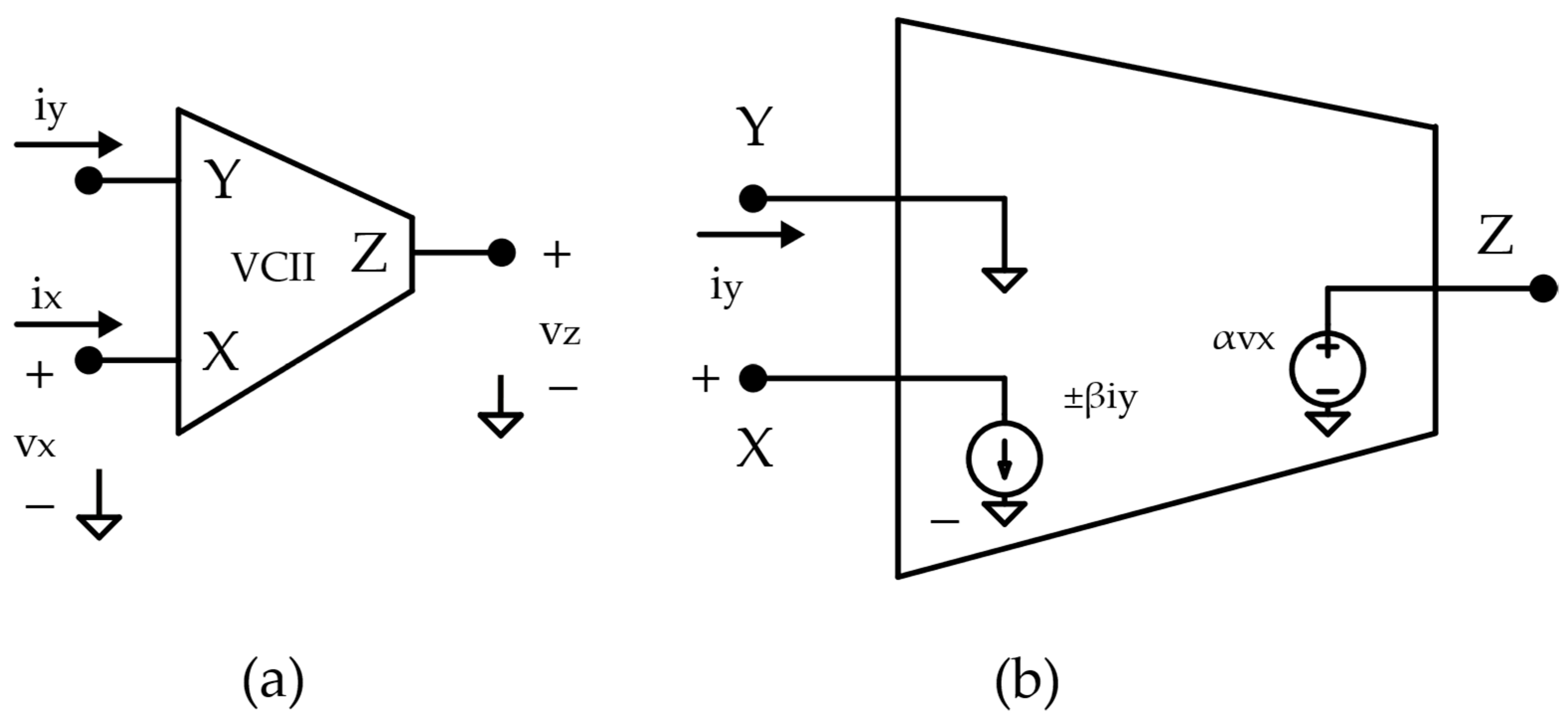
Figure 1 illustrates the symbol and equivalent circuit of the VCII, showing that an ideal VCII operates as a current buffer from the Y terminal to the X terminal and as a voltage buffer from the X terminal to the Z terminal. Specifically, Y is a low-impedance (ideally zero) current input, X is a high-impedance (ideally infinite) voltage input and current output, and Z is a low-impedance (ideally zero) voltage output. The ideal voltage–current relationships of a VCII are given by
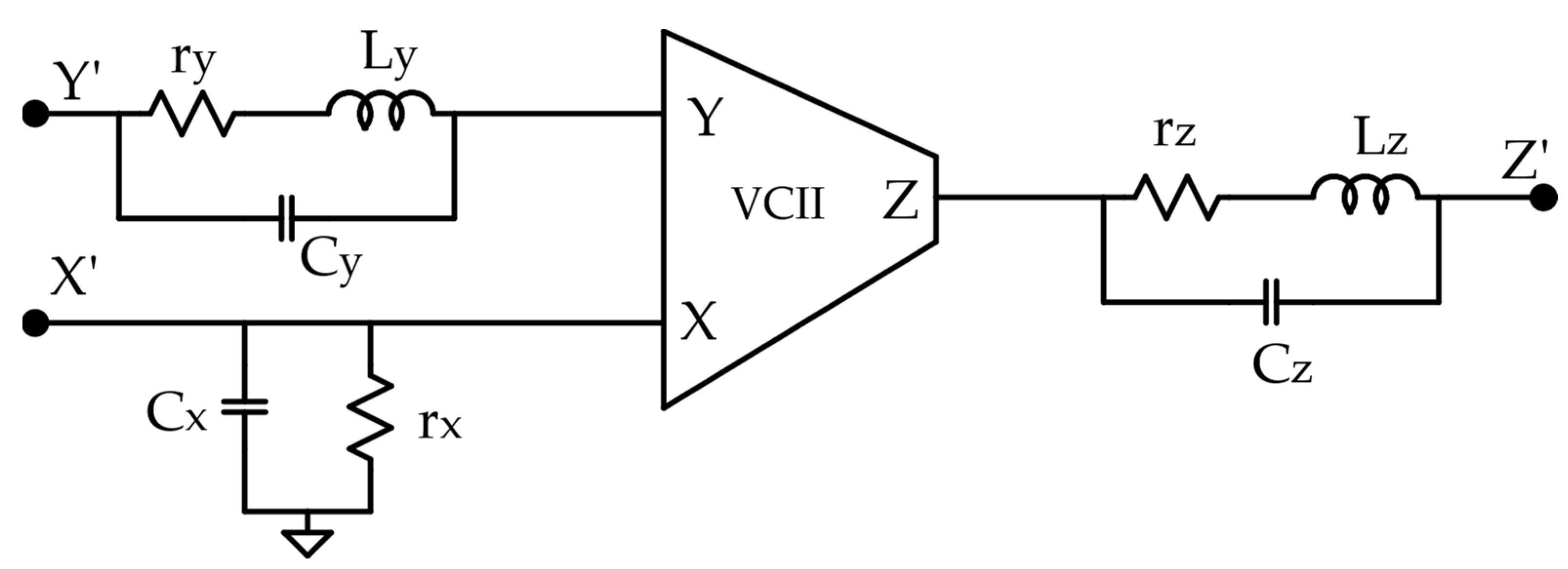
with α and β being ideally unitary gains. Depending on whether iX = +iY or iX = −iY, we classify the device as VCII+ or VCII−, respectively. Given the dual nature of the CCII and VCII, Y and Z terminals of a VCII have RLC-type parasitic impedances, while X parasitic terminal impedance is of the RC type, as shown in Figure 2.
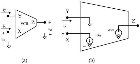
Figure 1.
Second-generation voltage conveyor (a) circuit symbol (b) equivalent circuit.
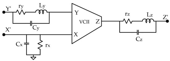
Figure 2.
Second-generation voltage conveyor with typical parasitic components.
3. Proposed VCII
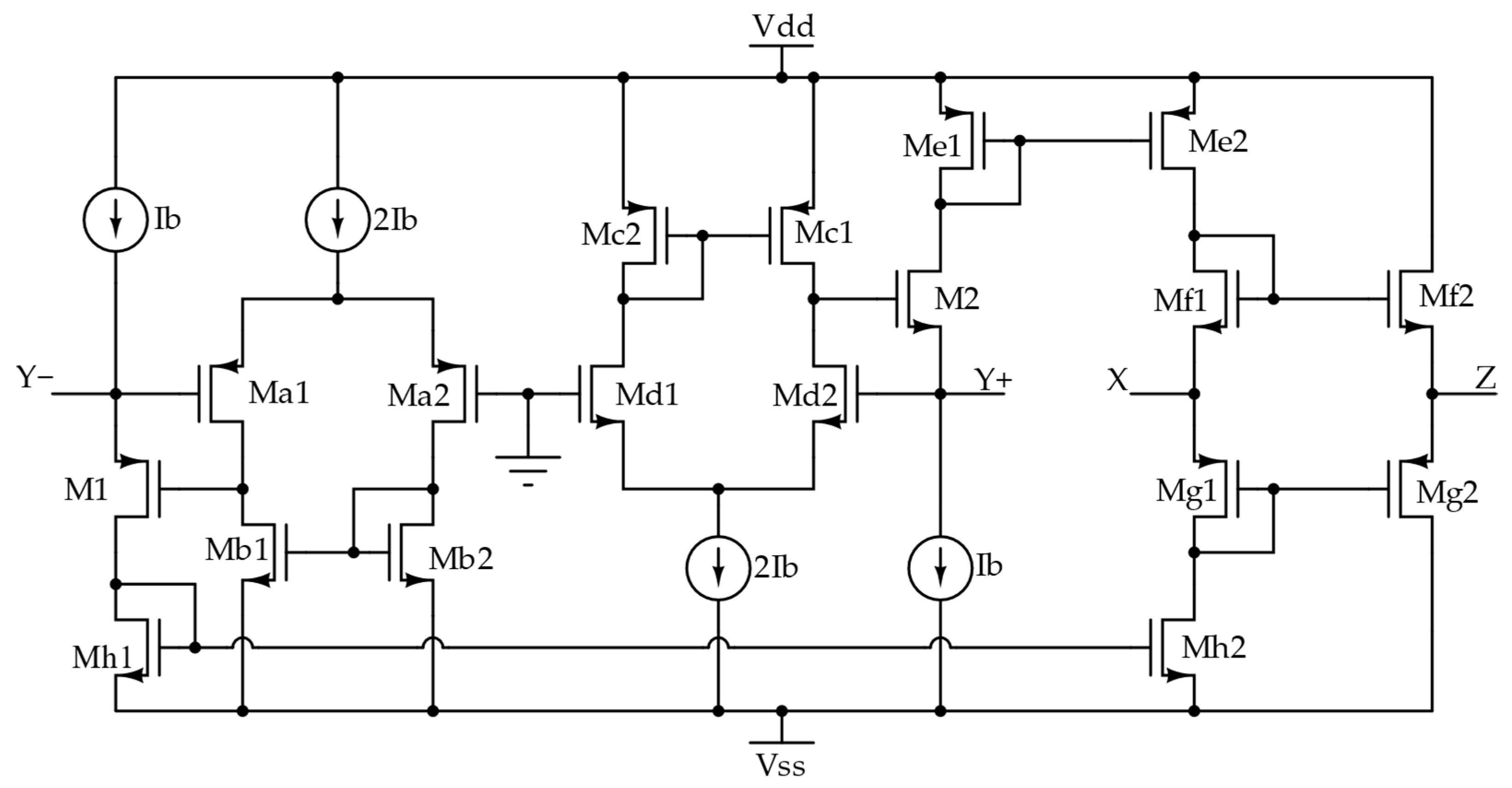
The design presented in this study introduces a transistor-level implementation of a VCII, specifically structured to include a voltage input terminal (X) and a voltage output terminal (Z), together with two current input terminals (Y+ and Y−).
The operation of the proposed VCII circuit is based on its current-mirroring structure, which enables it to output the sum of the input currents at terminal X. Current mirrors connected to Y+ and Y− stabilize terminal X when it is at rest.
When a current is applied to either Y+ or Y−, this current is mirrored onto X, with identical but opposite effects for Y+ and Y−, respectively. When both Y+ and Y− receive equal currents, the current at X doubles the input current on each terminal, representing the sum of the currents from Y+ and Y−.
This summed current at X is used to create an output voltage at terminal Z by taking advantage of the proprieties of the VCII. The output voltage is proportional to the summed current, as shown by
where is used as a gain resistor (in this case with a value of 100 kΩ) placed on terminal X. This relationship allows the VCII to produce a voltage output directly proportional to the sum of the currents on Y+ and Y−, enabling it to serve applications requiring cumulative current sensing. When an overall measurement of several sources is required, this summing function is especially helpful because it offers a practical way to translate summed current data into a corresponding voltage output at Z.
In Figure 3 the symbol of the proposed dual Y VCII is shown, and in (3) the relationships between voltages and current are reported.
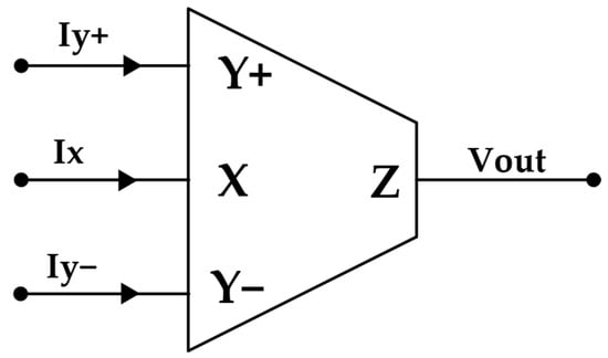
Figure 3.
Proposed dual Y VCII as block scheme.
The proposed circuit is built around a dual differential pair structure. The Y− terminal is defined by the first differential pair, which is made up of NMOS transistors, while the Y+ terminal is defined by the second differential pair, which is made up of PMOS transistors. These differential pairs serve to control the current flow and establish the mirrored behavior that enables the VCII to sum the input currents from Y+ and Y− at the X terminal. In this configuration, each differential pair splits the input current based on the voltage difference applied to its gates. The NMOS differential pair on Y− provides a low-impedance path for current, allowing it to respond quickly to variations in input current, while the PMOS pair on Y+ supplies a high impedance, creating complementary behavior between the two pairs. This complementary action allows the sum of the inputs on Y+ and Y− to be appropriately converted by the mirrored current on X. Transistors M1 and M2 are in a regulated common-gate configuration, so they are biased by the differential pairs voltages, providing the virtual ground at the Y+ and Y− terminals and reducing their impedances.
A voltage follower stage comes just after the differential pairs. Acting as a buffer, this stage keeps the output voltage at the target level without significantly loading the stages that come before it. By limiting the impact of the following stages and lowering the impedance that the remainder of the circuit perceives, the voltage follower stabilizes the output and makes sure that the summed current is accurately converted to a voltage output at terminal Z. Accurate voltage conversion and current summing are made possible by this design, which combines dual differential pairs with a voltage follower to provide exact and reliable input current summation.
The circuit configuration, at the transistor level, is shown in Figure 4.
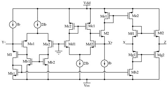
Figure 4.
The proposed dual Y VCII configuration at the transistor level.
4. Simulation Results
Simulations were performed employing 0.35 μm CMOS technology through the LTSpice simulator. Transistor dimensions are shown in Table 1; all transistors are sized for optimization of terminal impedances and mid-dynamic biasing. Supply voltages were set to ±0.9 V, while bias current was set to 3 μA. In the proposed design, the current sources in the original circuit have been replaced in simulation with current mirrors, all with an aspect ratio of 100 μm/1.4 μm, to achieve a more realistic representation of practical circuit behavior. Each differential pair receives double the input bias current thanks to the precise sizing of these current mirrors. This adjustment in mirror sizing maintains the desired operating conditions for both differential pairs, enhancing the accuracy of the simulated performance and reflecting a more practical implementation of the VCII circuit.

Table 1.
Transistor sizes.
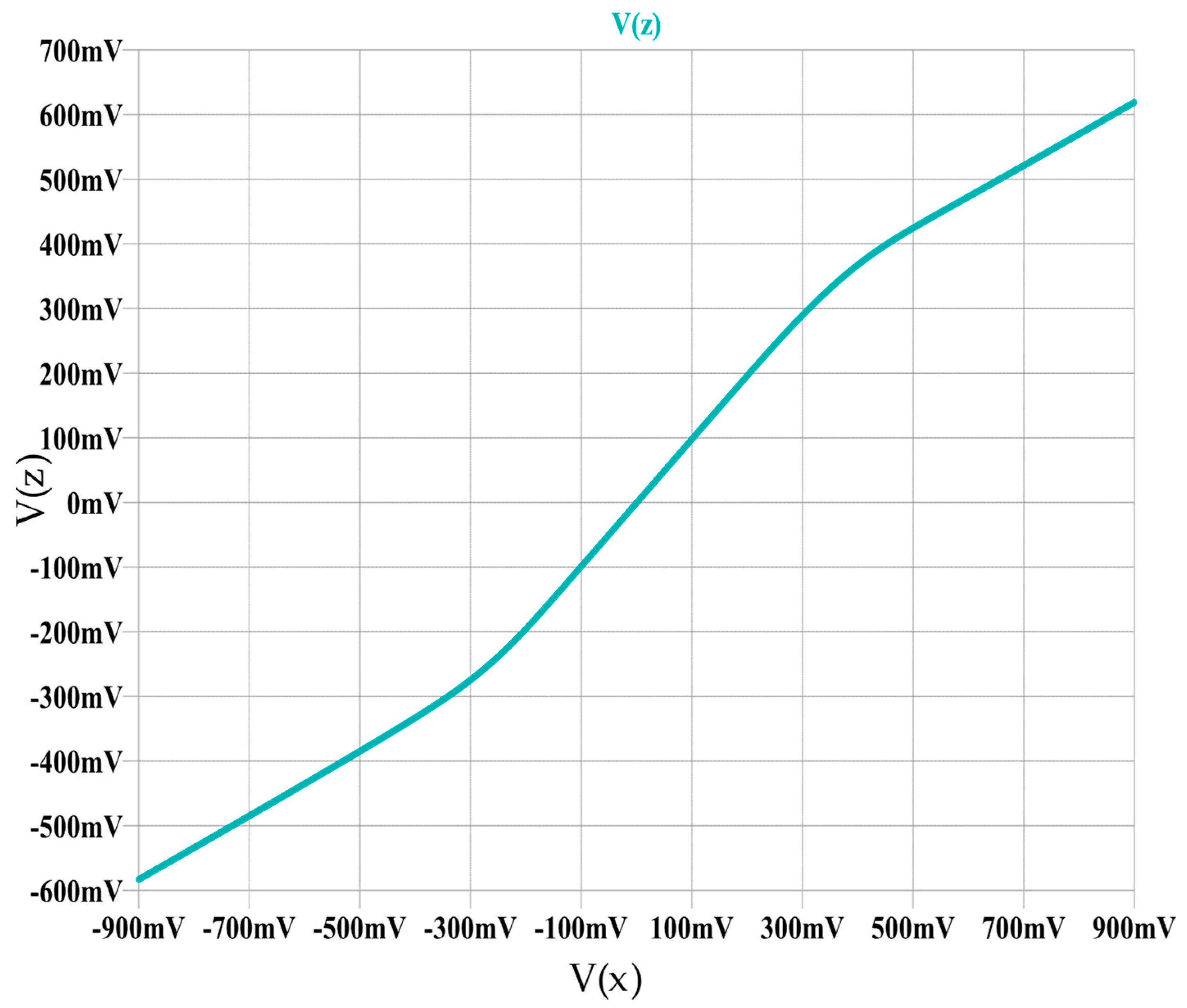
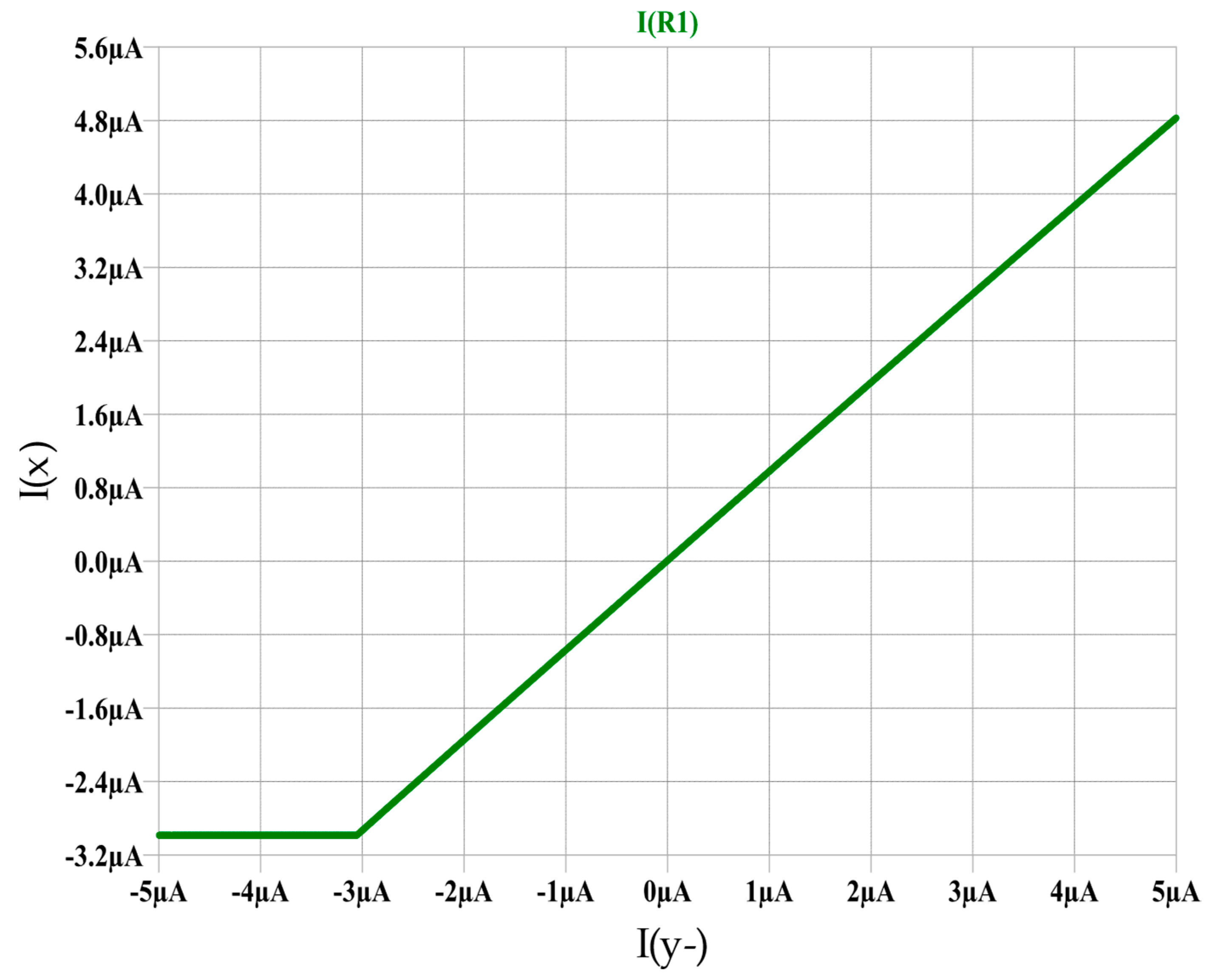
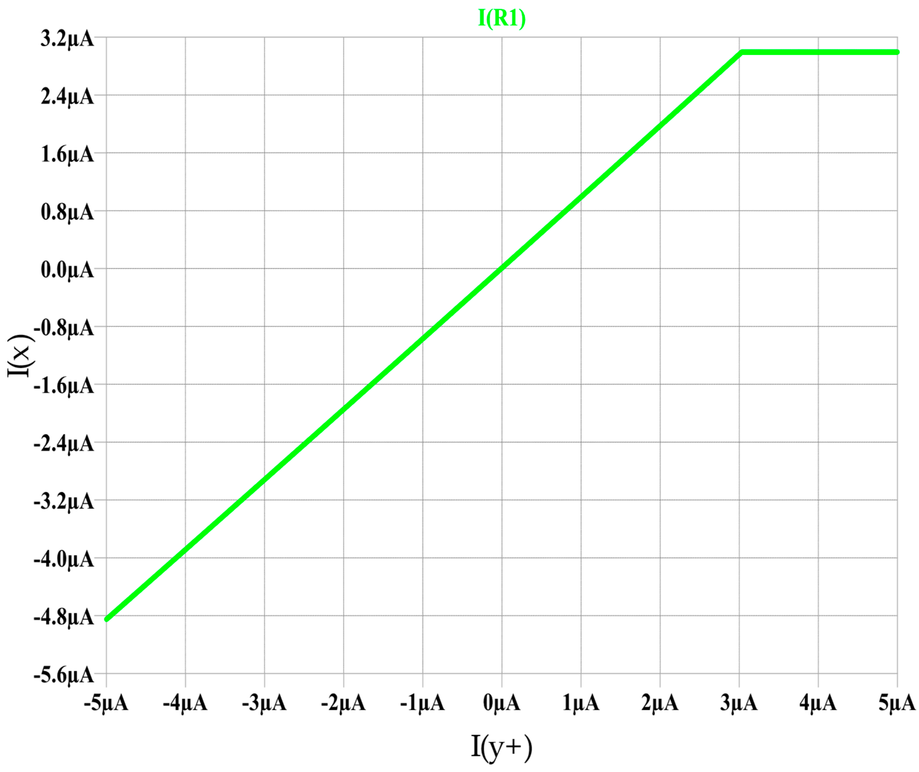
In Figure 5, Figure 6, and Figure 7, the DC performances of , and parameters are shown, respectively. To assess the first parameter, a varying input voltage was applied at the X terminal, oscillating between the negative and positive supply voltages. The results indicate that the parameter α consistently remains linear between −300 mV and +300 mV, determining this range as the output operating range. Similarly, the behavior of the two β parameters was analyzed by applying a current, sweeping between −5 μA and 5 μA, to the Y correspondent port and measuring the resulting current at the X port under different input current conditions.

Figure 5.
DC performances of the α parameter; V(z) vs. V(x).
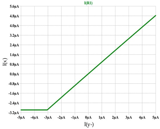
Figure 6.
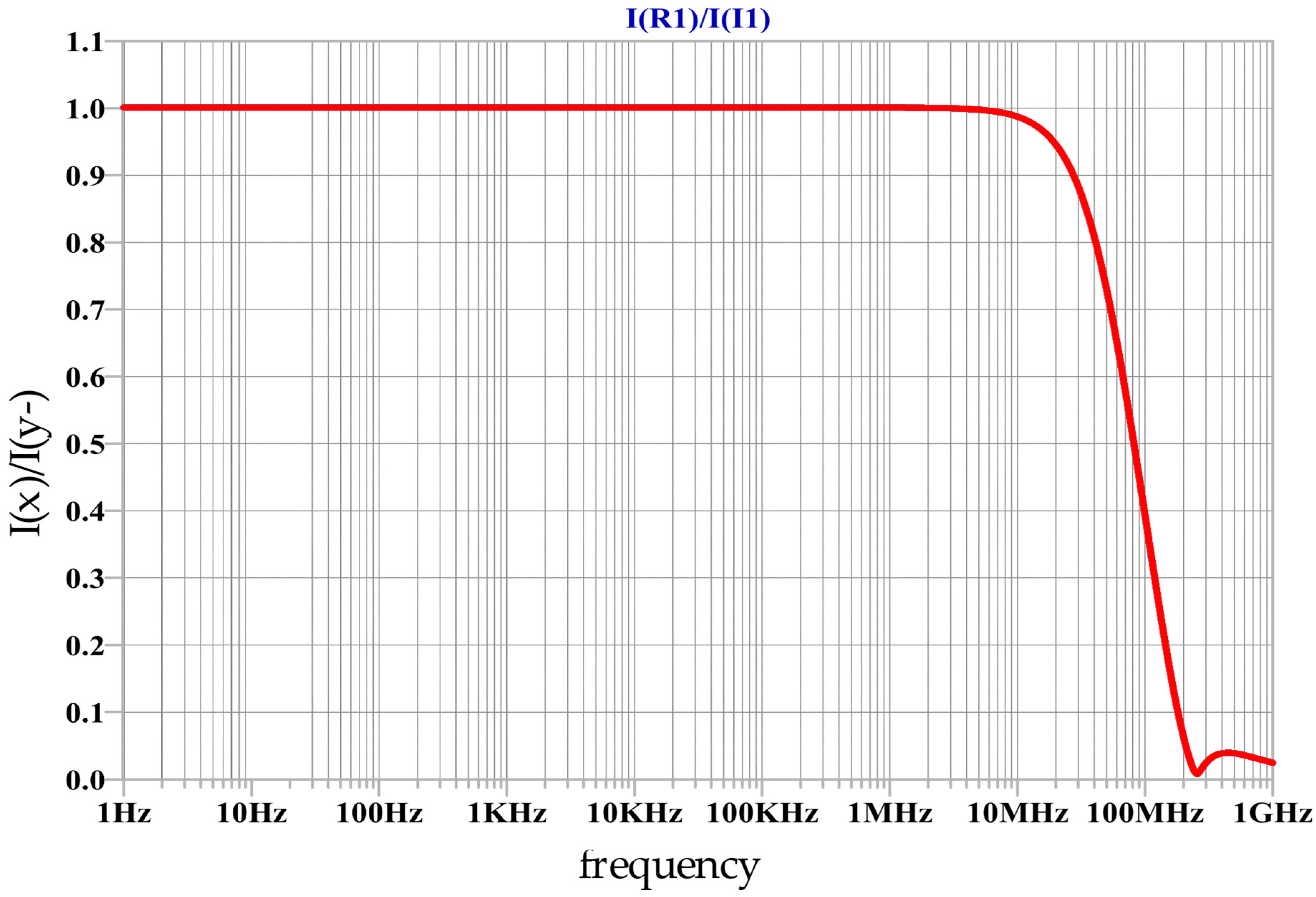
DC performances of the β+ parameter; I(x) vs. I(y−).
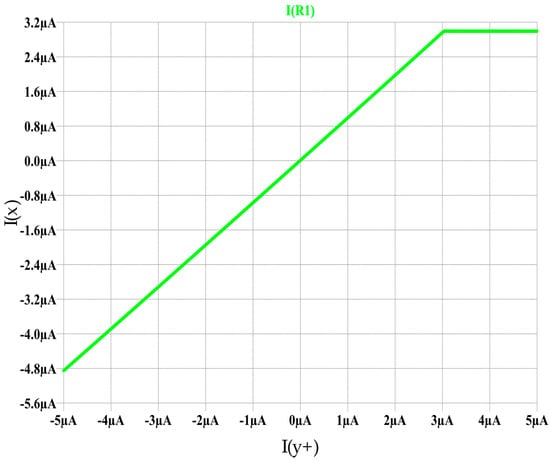
Figure 7.
DC performances of the β− parameter; I(x) vs. I(y+).
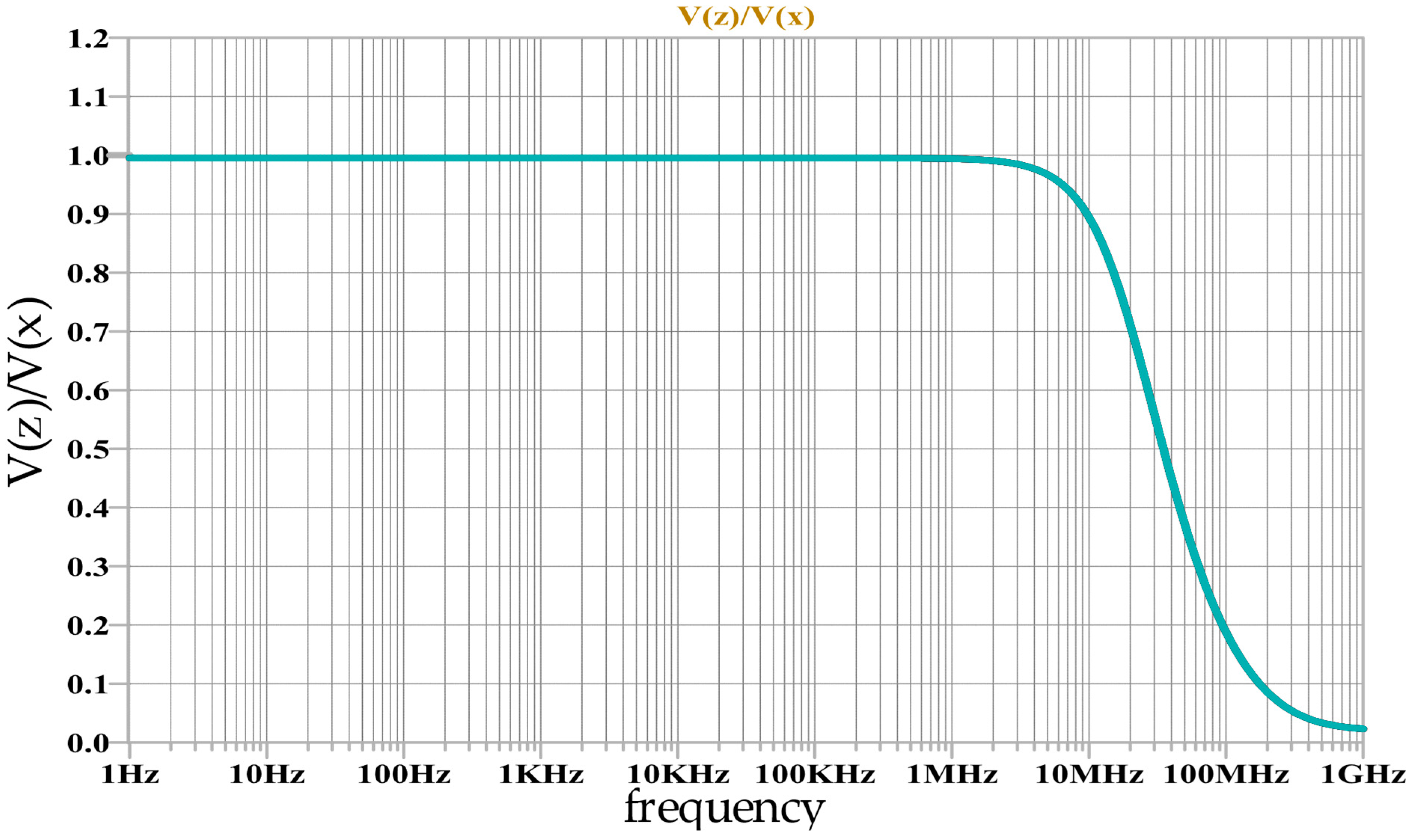
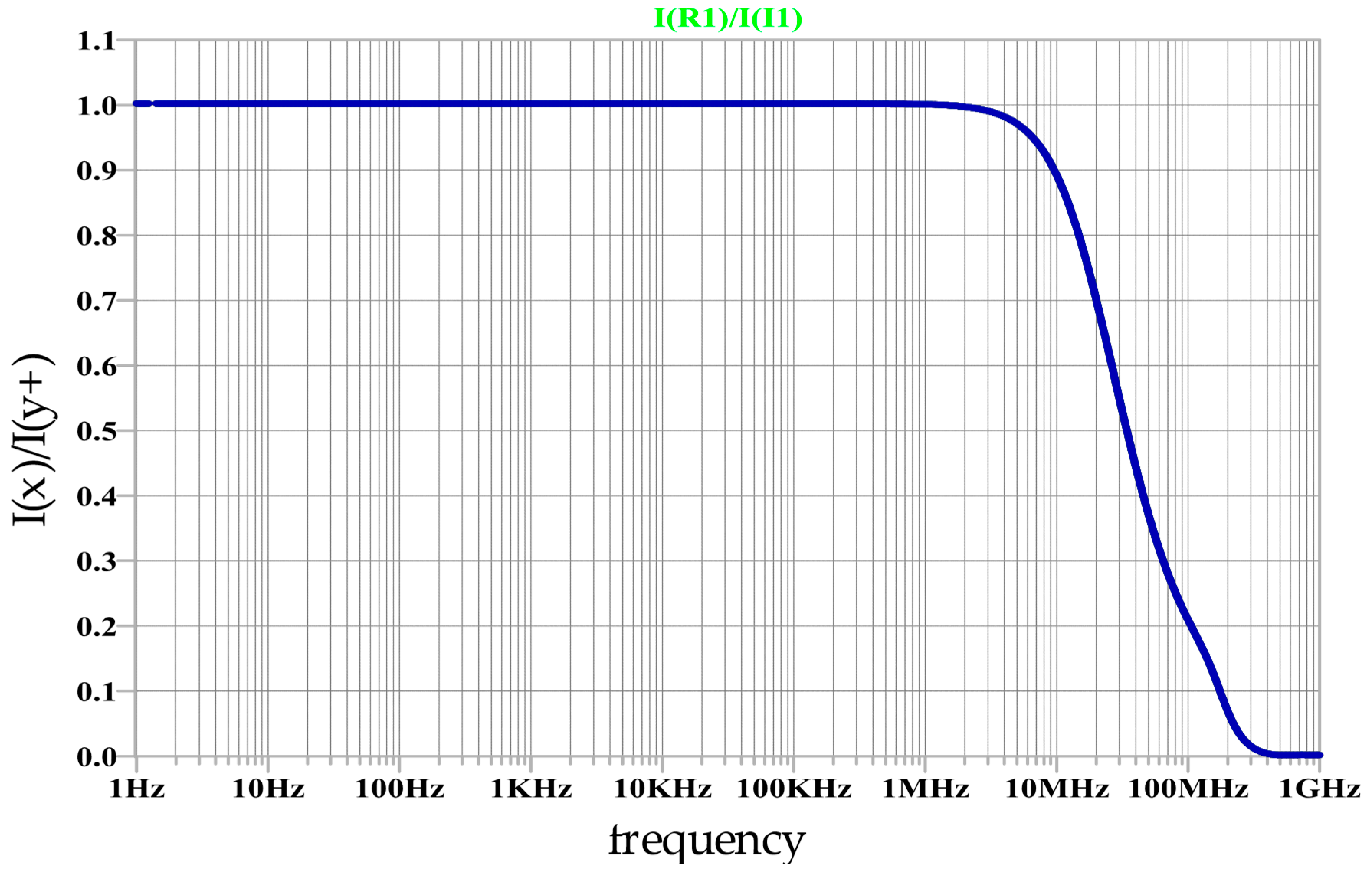
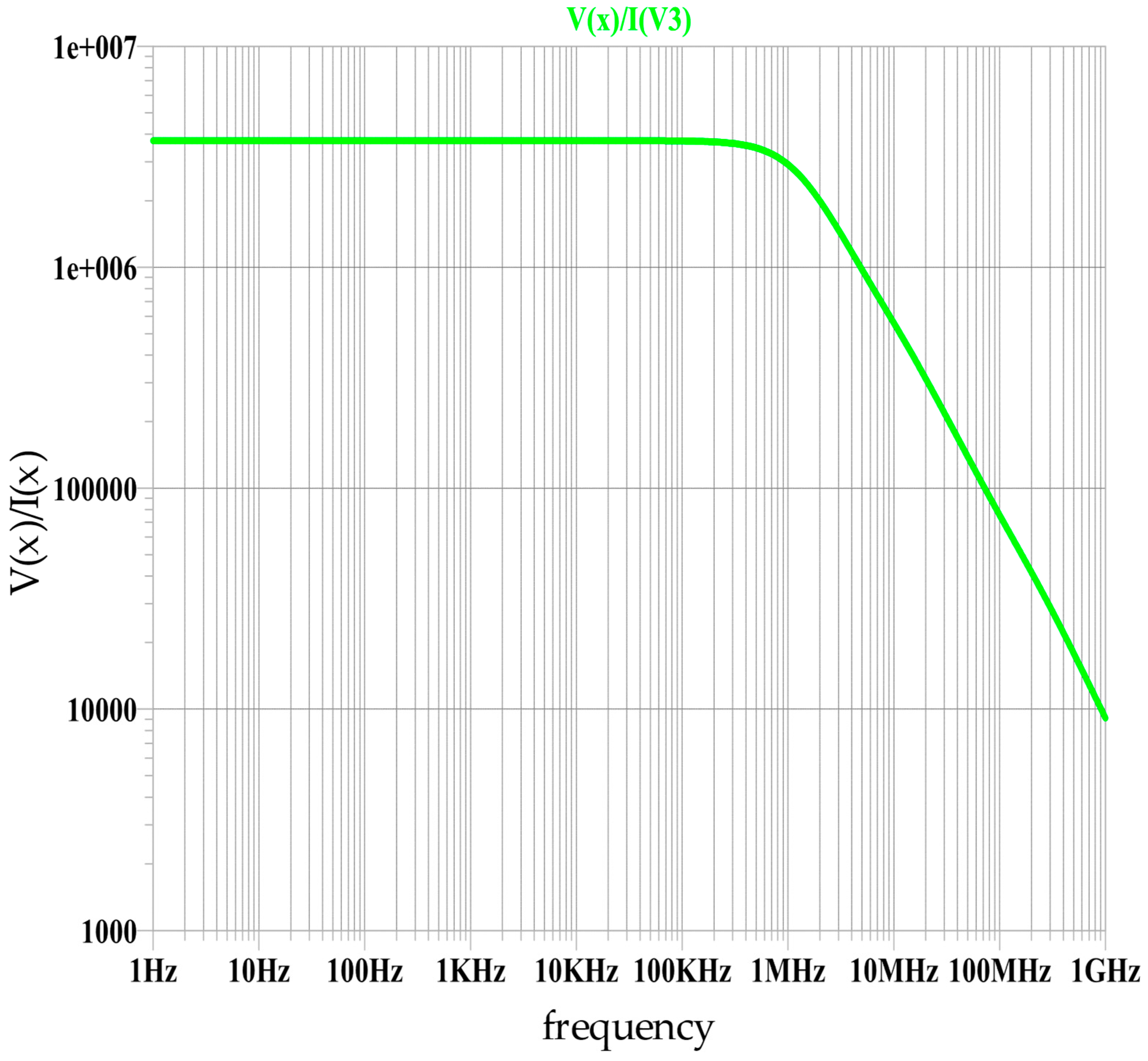
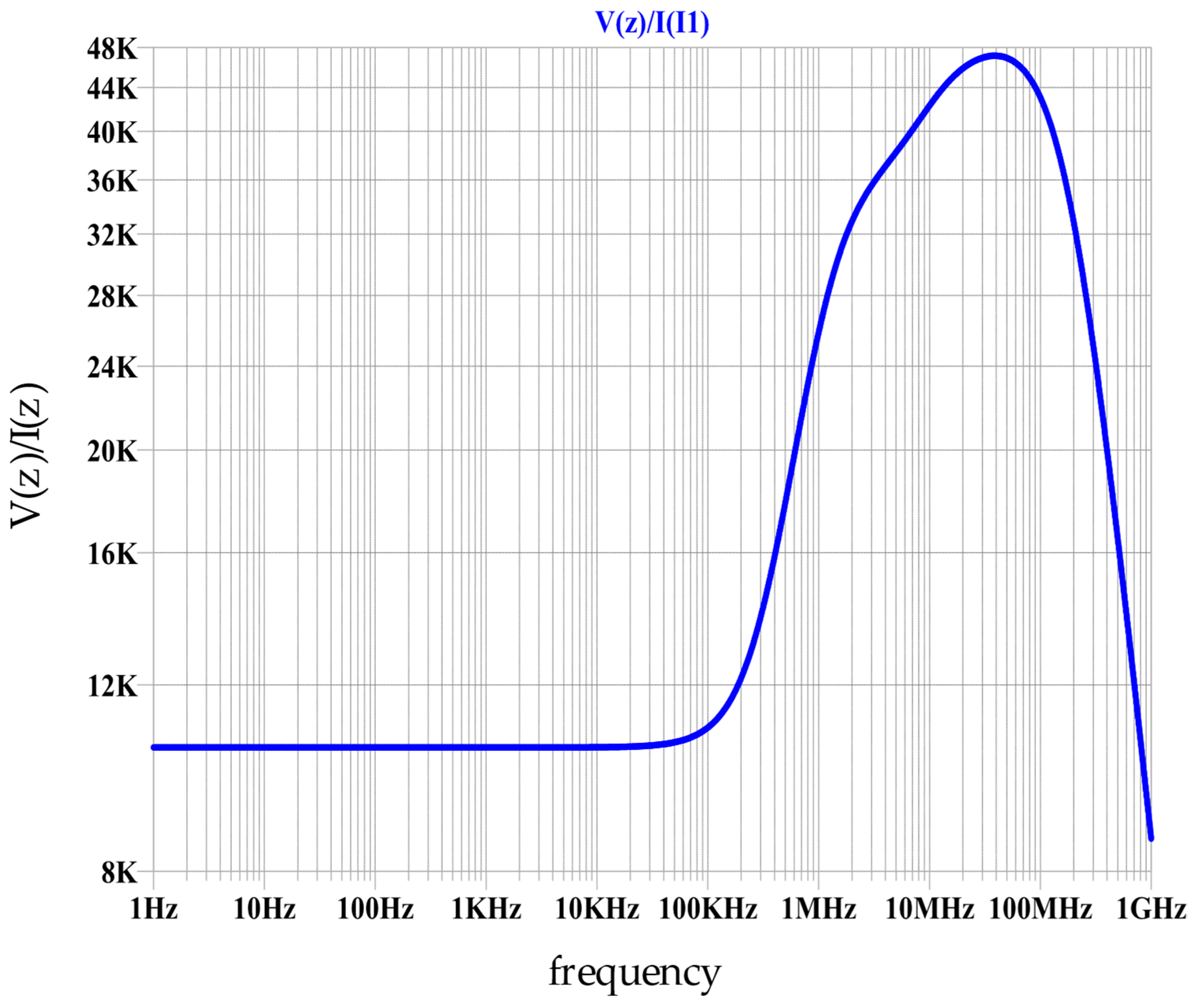
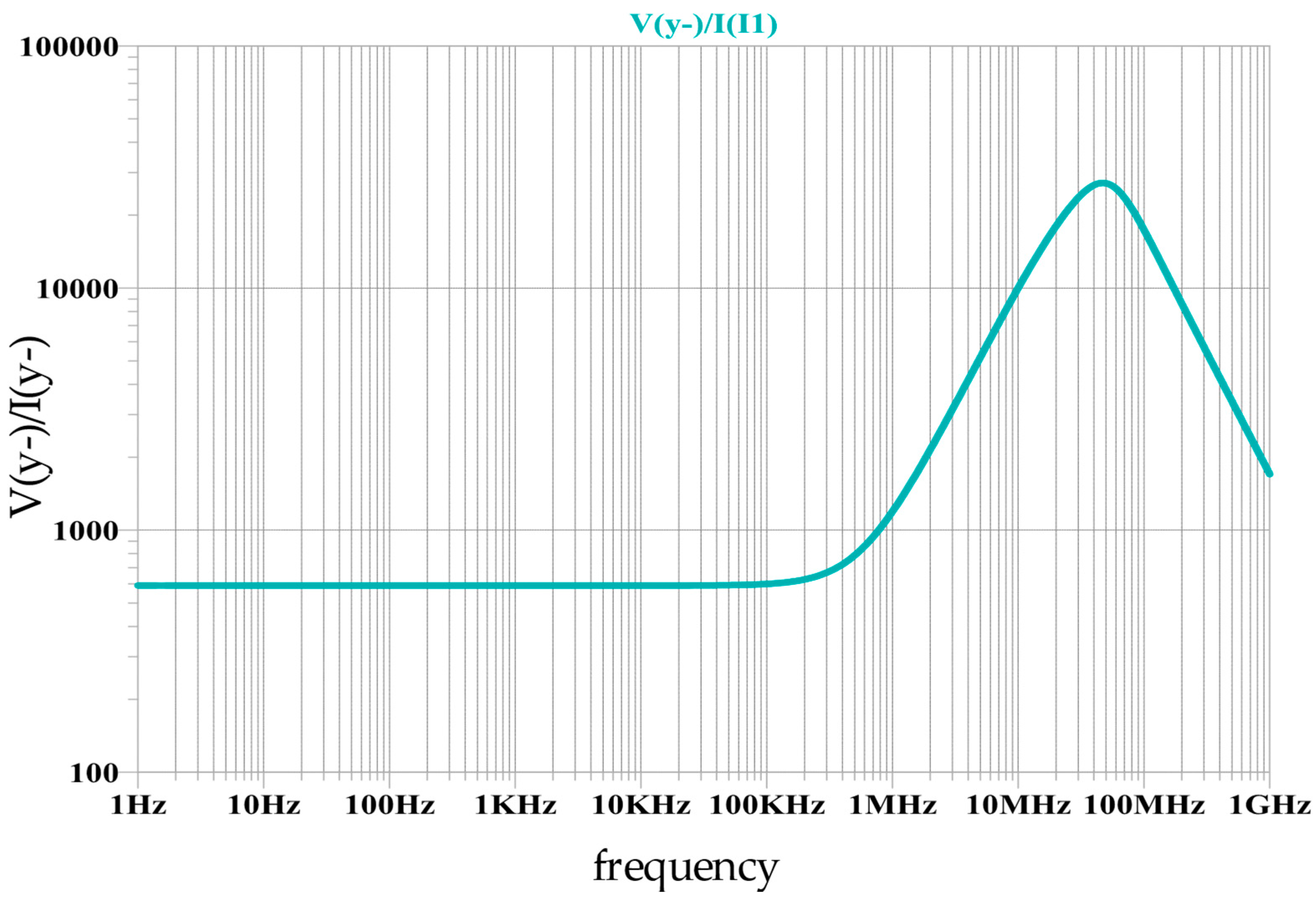
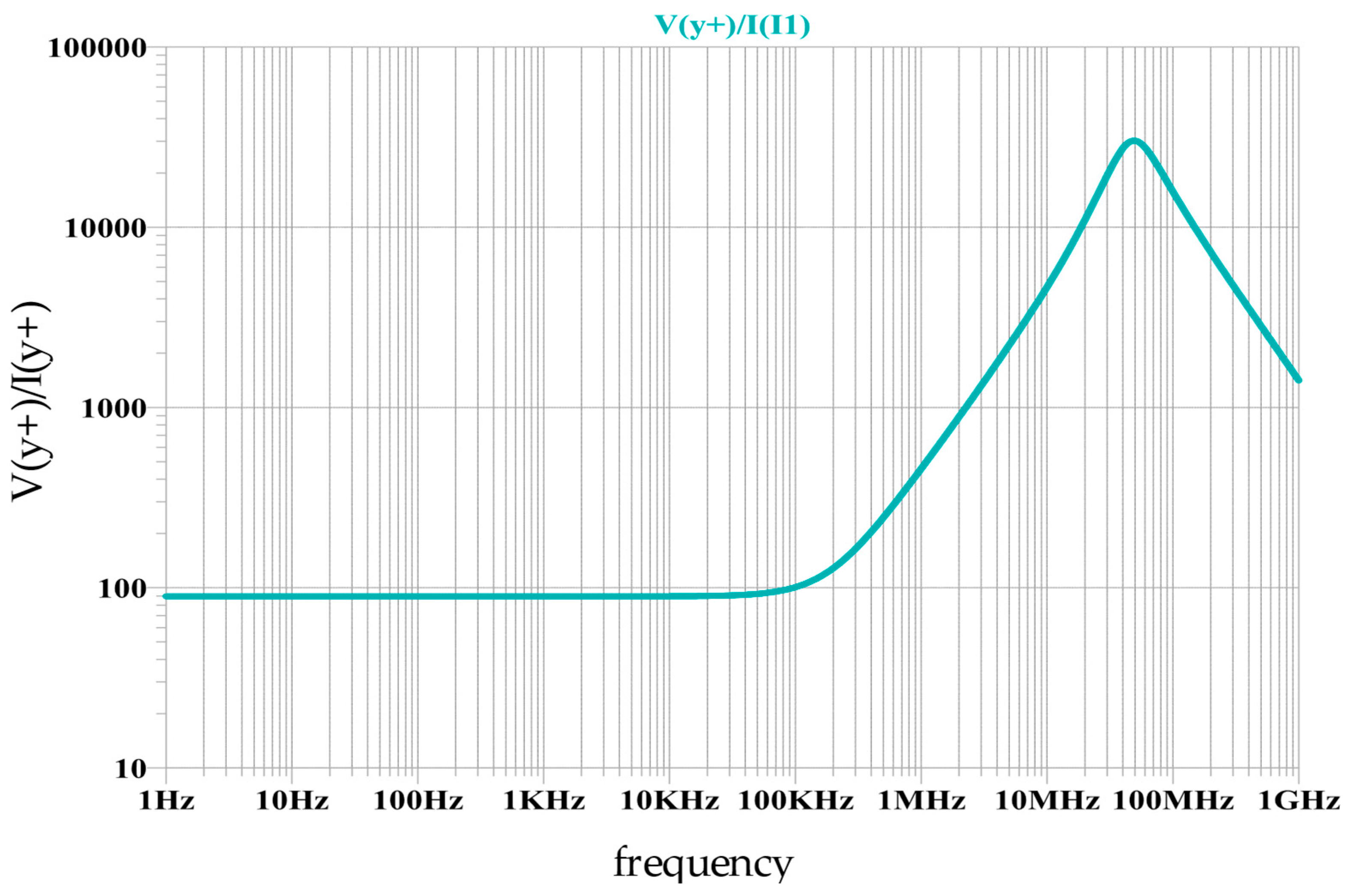
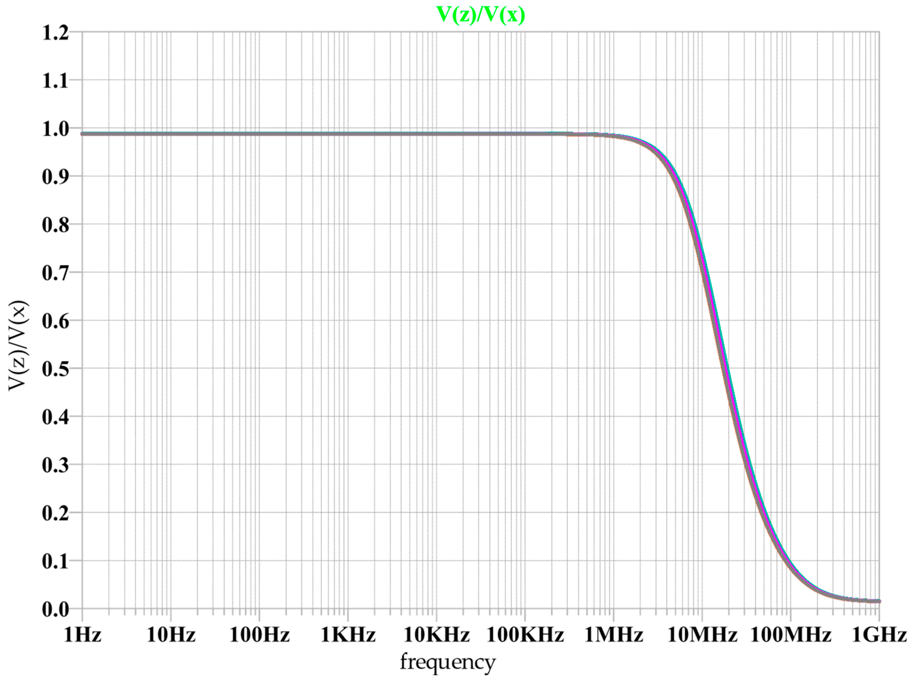
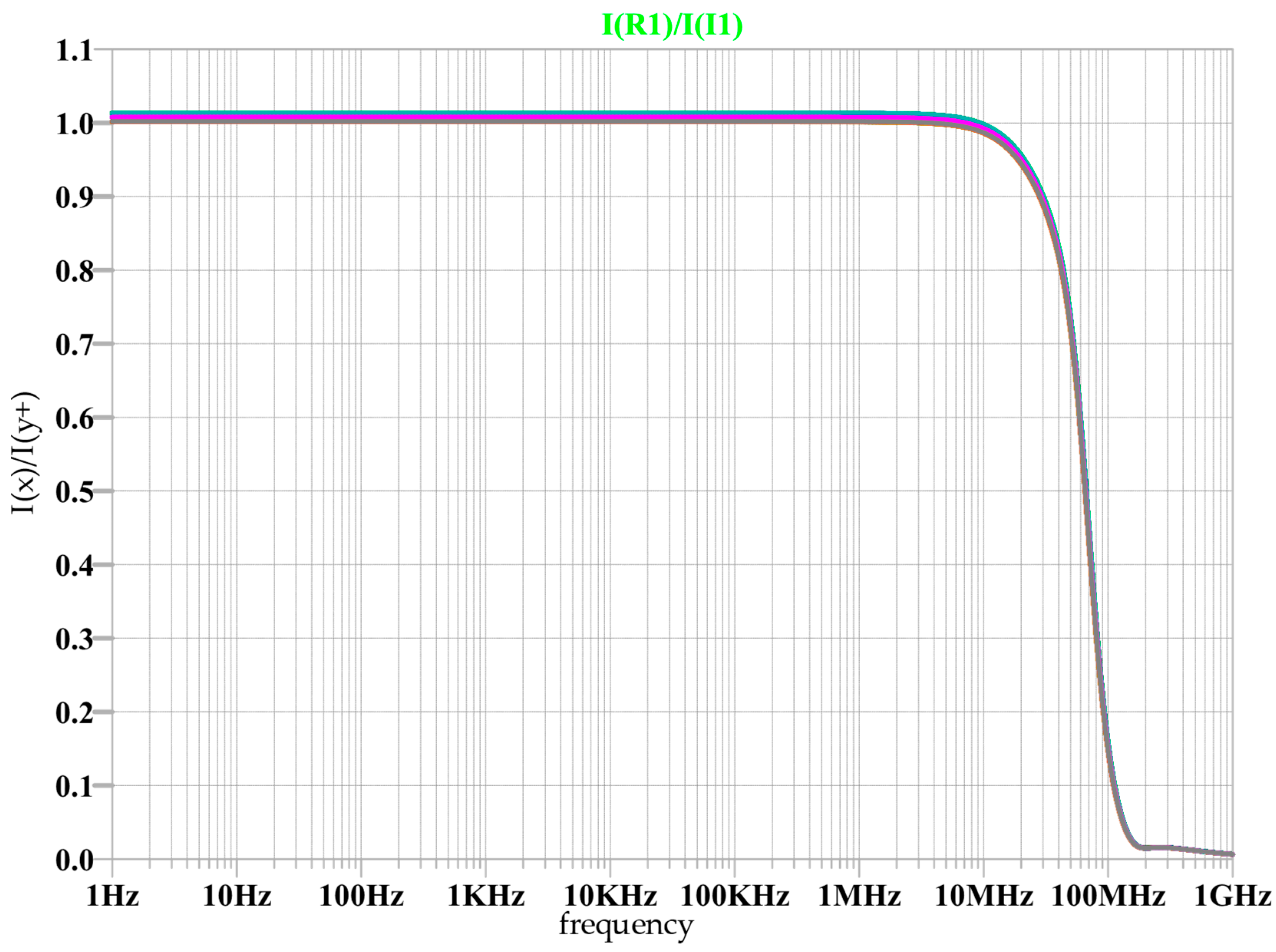
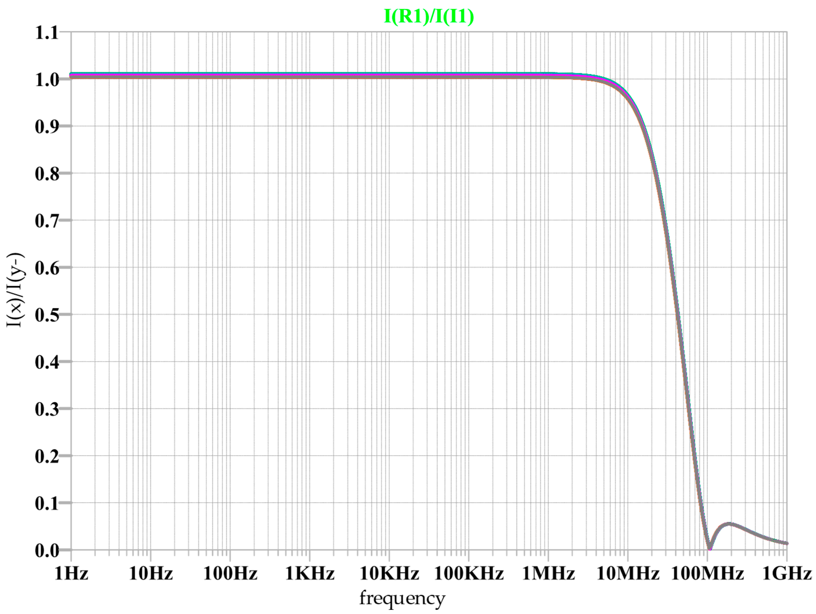
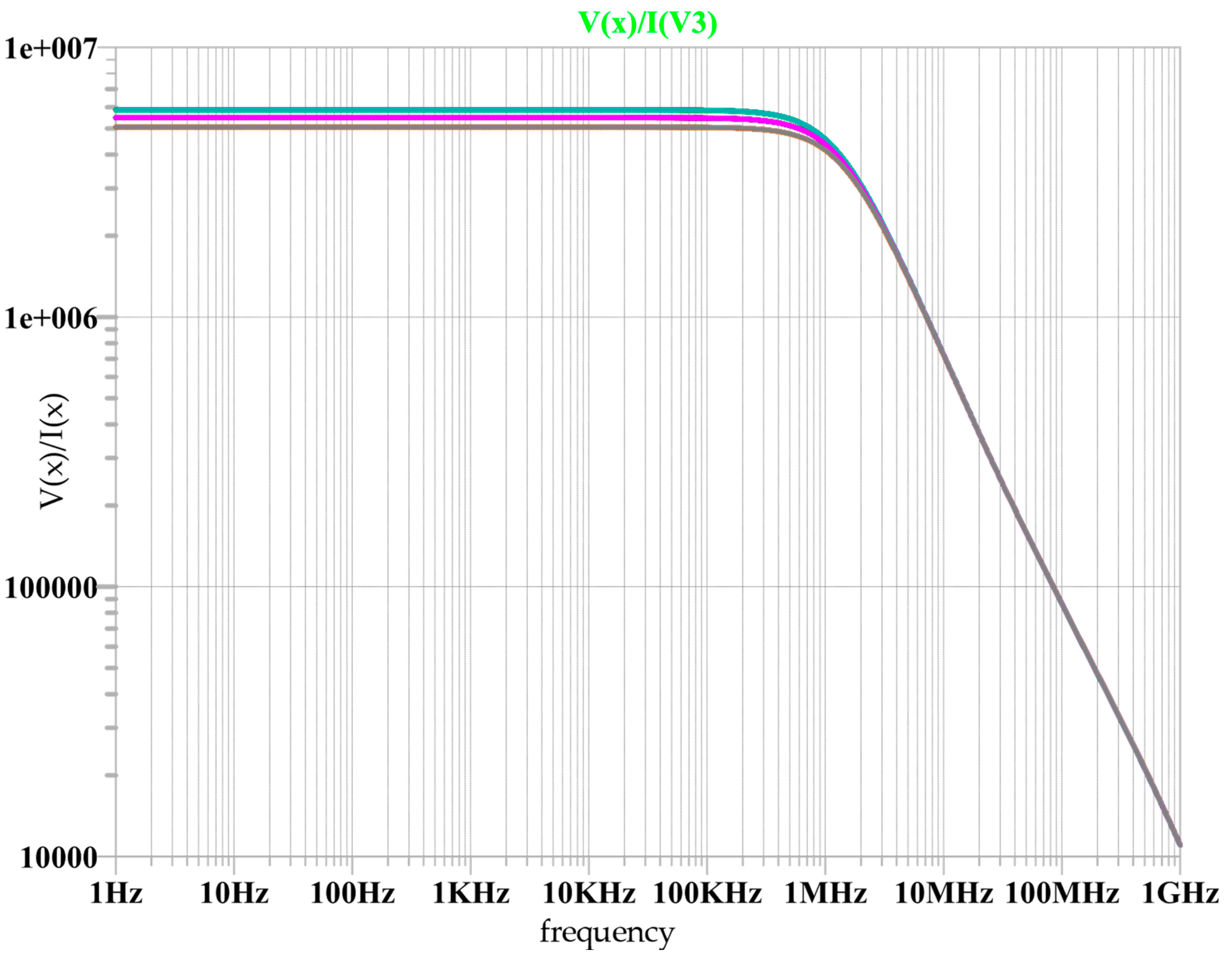
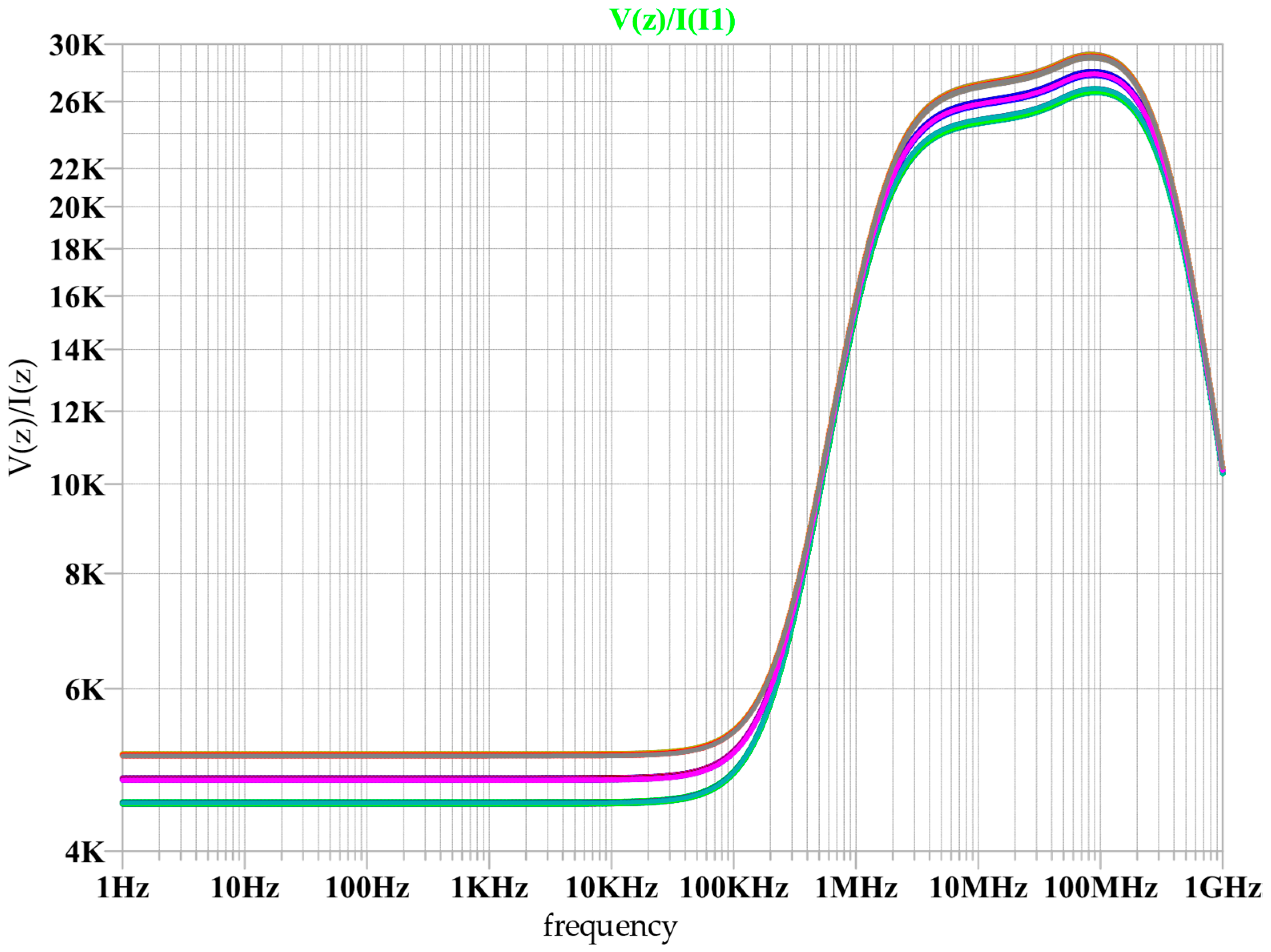
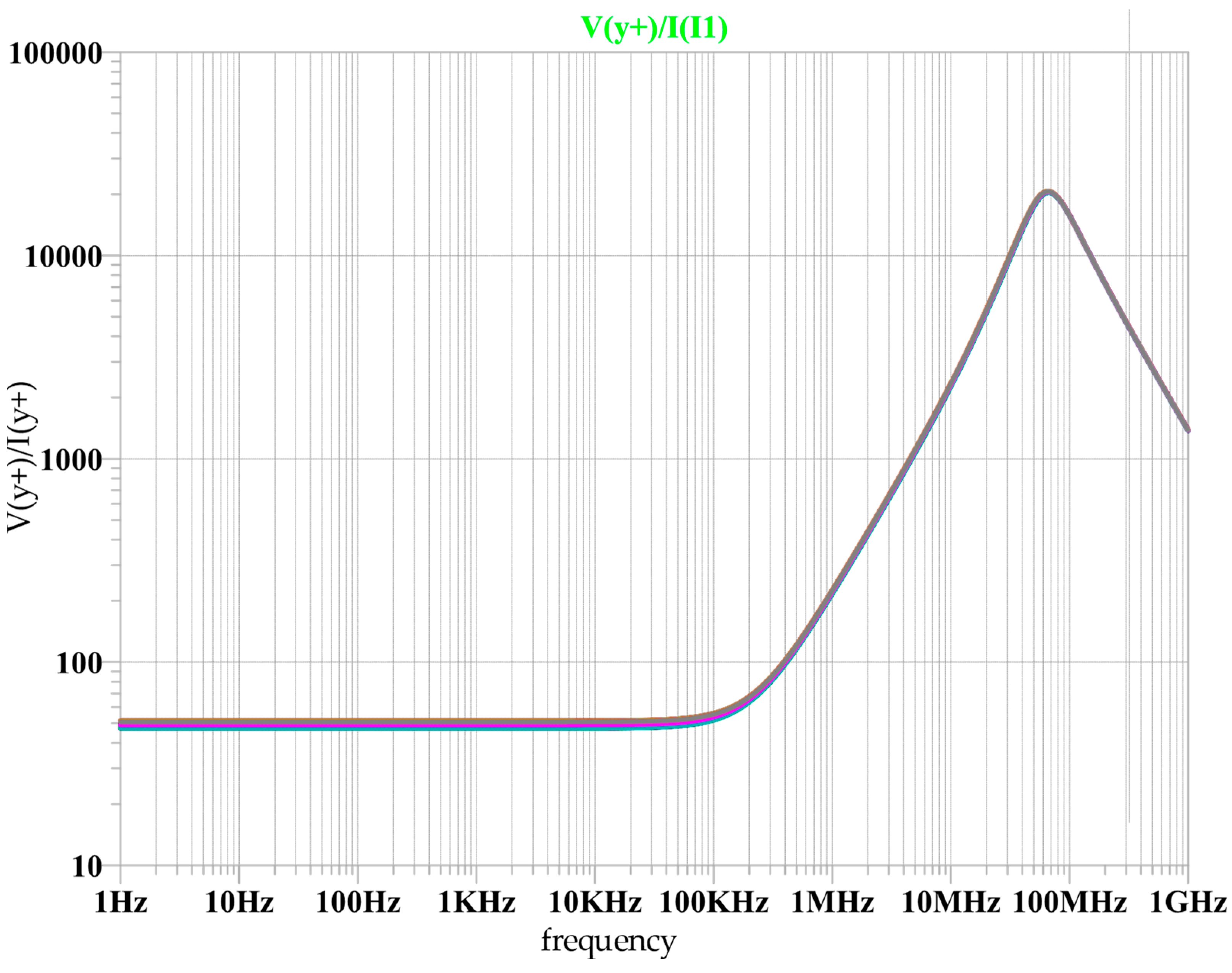
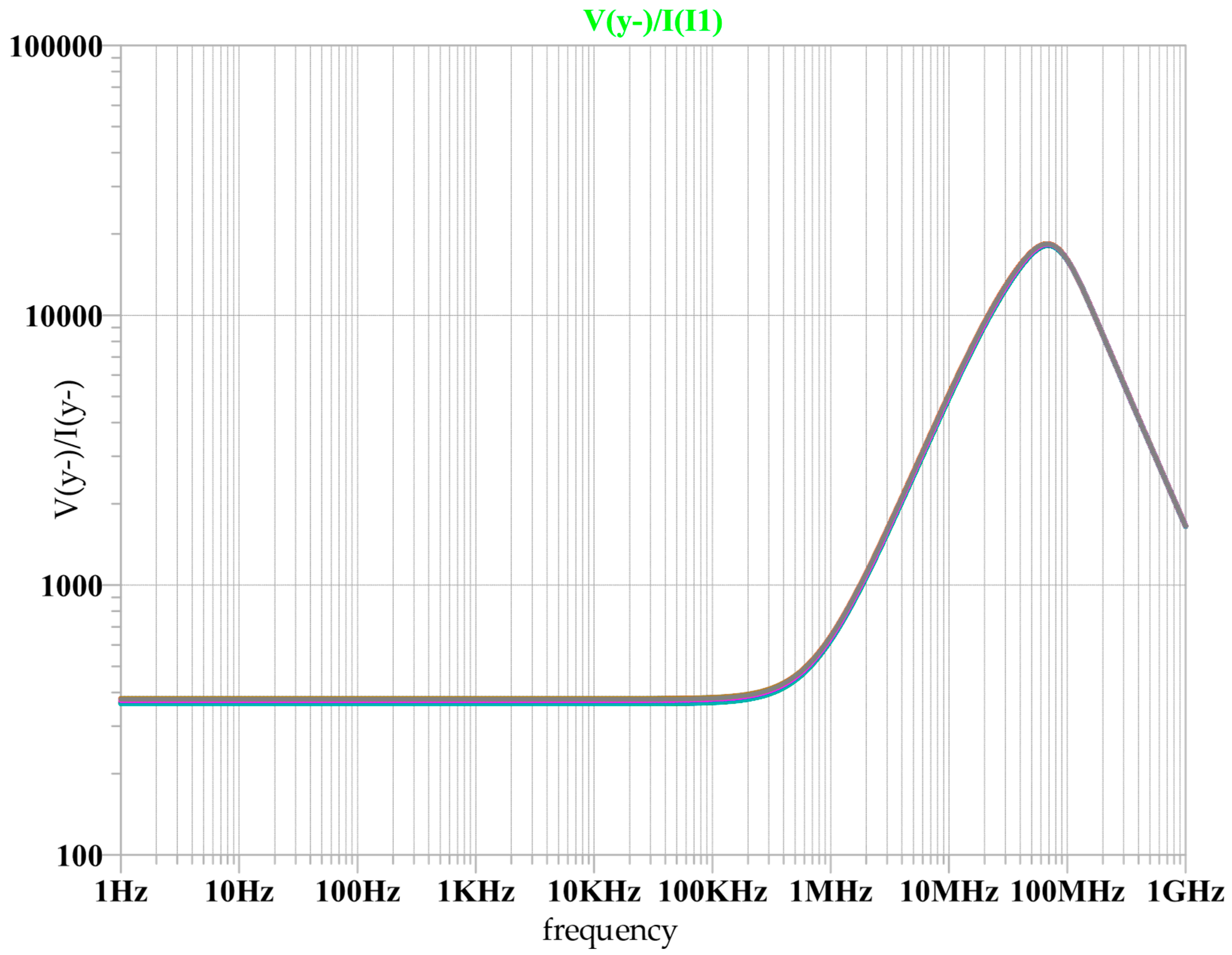
Frequency performances of the voltage conveyor are presented in Figure 8, Figure 9, and Figure 10, respectively. In detail, the transfer function is reported in Figure 8 and was evaluated with a 3 pF load at the output Z terminal; the bandwidth is 20 MHz. The bandwidth for and is, respectively, 51 MHz and 53 MHz. Terminal impedances were also shown in Figure 11, Figure 12, Figure 13 and Figure 14; the resulting impedance values are 3.7 MΩ at the X terminal, 90 Ω at the Y+ terminal, 600 Ω at the Y−, and 10.4 kΩ at Z (all impedances were evaluated at 1 a KHz frequency). All the reported parameters are summarized in Table 2, Table 3 and Table 4.
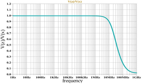
Figure 8.
AC performances of the α parameter with a 3 pF capacitor connected to the Z node; V(z)/V(x) vs. frequency.
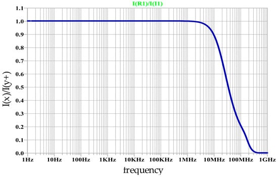
Figure 9.
AC performances of the β+ parameter; I(x)/I(y+) vs. frequency.
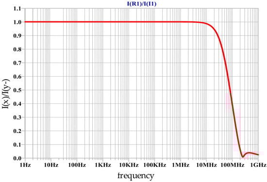
Figure 10.
AC performances of the β− parameter; I(x)/I(y−) vs. frequency.
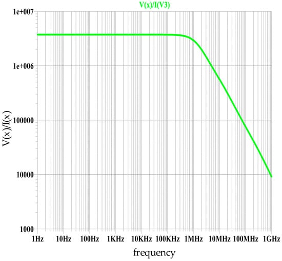
Figure 11.
Proposed VCII X terminal impedance vs. frequency.
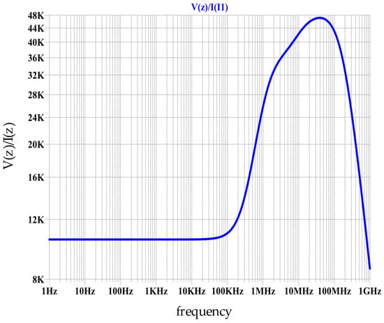
Figure 12.
Proposed VCII Z terminal impedance vs. frequency.
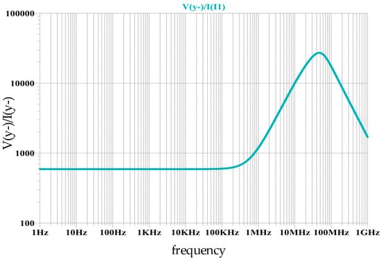
Figure 13.
Proposed VCII Y− terminal impedance vs. frequency.
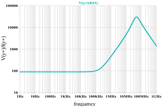
Figure 14.
Proposed VCII Y+ terminal impedance vs. frequency.
Table 2.
Proposed dual Y VCII performance parameters.
Table 3.
Parasitic parameters summary.
Table 4.
Low frequency impedance values of the proposed dual Y VCII.
The parasitic parameters of the proposed VCII were determined and reported in Table 3, considering a capacitance on terminal X, a capacitance and an inductance on the two terminals Y and Z. The terminal impedance values for low frequency are shown in Table 4. Finally, in Table 4 impedance values for low frequency are reported.
In Figure 15, Figure 16, Figure 17, Figure 18, Figure 19, Figure 20 and Figure 21, the corner analyses on the main VCII parameters (α, β+, β−, X impedance, Z impedance, Y+ impedance, and Y− impedance, respectively) are reported.
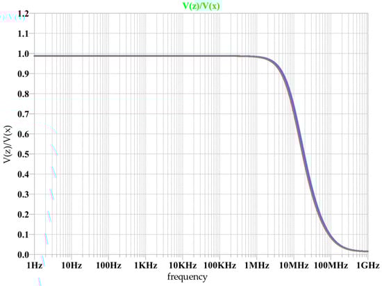
Figure 15.
Corner analysis of AC performances of α parameter.
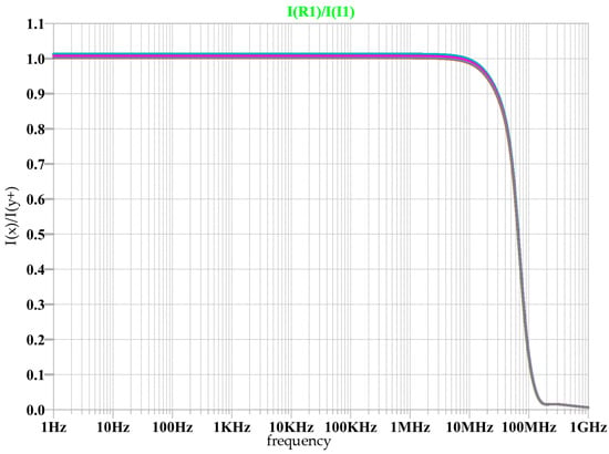
Figure 16.
Corner analysis of AC performances of β+ parameter.
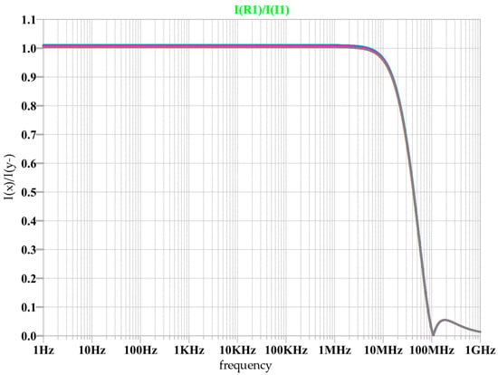
Figure 17.
Corner analysis of AC performances of β− parameter.

Figure 18.
Corner analysis of the proposed VCII X terminal impedance.
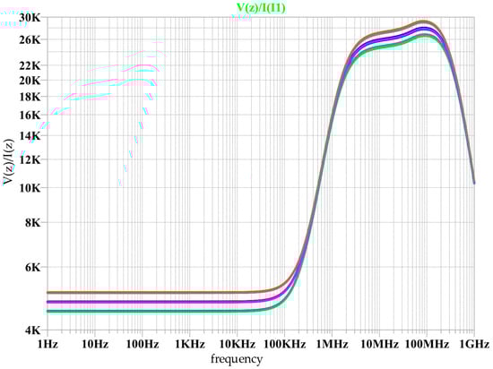
Figure 19.
Corner analysis of the proposed VCII Z terminal impedance.
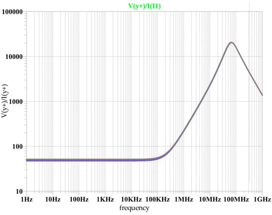
Figure 20.
Corner analysis of the proposed VCII Y+ terminal impedance.
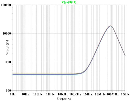
Figure 21.
Corner analysis of the proposed VCII Y− terminal impedance.
The temperature sweep has been (−20 °C, 80 °C), while the supply voltage has been varied by ± 10% from the nominal value. Montecarlo analysis has concerned the threshold voltages and oxide thickness of nMOS and pMOS transistors. In all the corner analyses performed, the variation in VCII parameters is low.
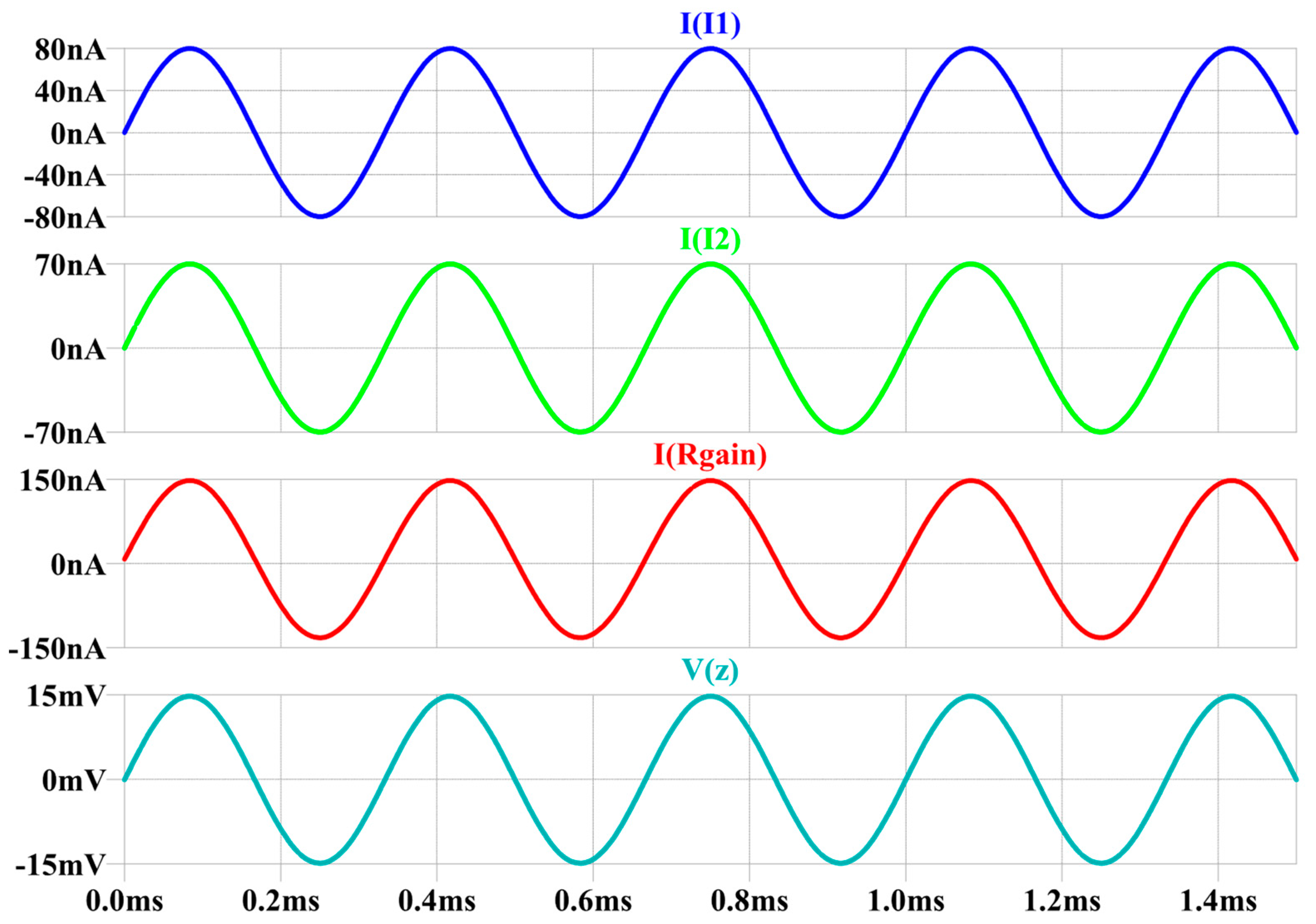
In Figure 22, LTspice simulations for a sample case are reported. Two current generators with input currents of 80 nA and 70 nA peak-to-peak and a 3 kHz frequency are used, connected to terminals Y+ and Y− of the VCII. The sum of the currents of the generators is evaluated on a gain resistor RGAIN, placed on terminal X. The resulting conversion to voltage and the amplification by the resistor RGAIN, chosen in this case to be 100 kΩ, is checked on the output terminal Z.
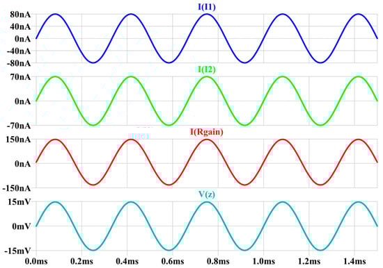
Figure 22.
Summing operation of the proposed dual Y VCII.
The proposed circuit power consumption is about 24.6 µW. This outcome highlights the circuit’s suitability for low-power applications where energy efficiency is essential, like environmental monitoring systems and biomedical devices. The proposed solution can be used also as a floating dual-input amplifier or as a transimpedance amplifier (TIA).
5. Conclusions and Future Works
In applications such as power management systems, sensor array data, and environmental monitoring, where cumulative readings are helpful, this setup provides clear benefits. The proposed dual Y VCII can be successfully included in systems requiring precision and energy efficiency because of its low power consumption, high accuracy, and solid performance. Additionally, the summing capability of the VCII, demonstrated through simulations, highlights its potential to simplify circuit designs for aggregating current measurements. This novel technology is especially well-suited for applications like battery management systems, environmental pollution monitoring, and biomedical devices like glucose biosensors and EEG electrodes because in these applications it is usual to collect signals, for instance currents, from several sensors to monitor various parameters. In order to increase integration into modern electronic systems, future work may concentrate on further optimizing the circuit performance, such as increasing its bandwidth, lowering parasitic effects, and modifying the design for the newest CMOS technology.
Author Contributions
Conceptualization, D.C. and G.B.; validation, G.F.; formal analysis, R.O.; data curation, R.O.; writing—original draft, R.O.; writing—review and editing, R.O., D.C., G.B., V.S., and G.F.; supervision, V.S. and G.F. All authors have read and agreed to the published version of the manuscript.
Funding
This research received no external funding
Data Availability Statement
The original contributions presented in this study are included in the article.
Conflicts of Interest
The authors declare no conflict of interest.
References
- Palumbo, G.; Pennisi, S. A High-performance CMOS CCII. Int. J. Circuit Theory Appl. 2001, 29, 331–336. [Google Scholar] [CrossRef]
- Bhargave, G.; Sheokand, P.; Kaur, J. A New Low Voltage and Low Power Filter Using DTMOS-CCII. In Proceedings of the 2015 Second International Conference on Advances in Computing and Communication Engineering, Dehradun, India, 1–2 May 2015; IEEE: Dehradun, India; pp. 17–20. [Google Scholar]
- Yeo, K.S.; Roy, K. Low-Voltage, Low-Power VLSI Subsystems: New Approaches to Silicon-Level Design for Low-Power Circuitry Pacing Electronics and ICs; Low-Power Solutions for Adders, Multipliers, ROMs, SRAMs, DRAMs, and Signal Processors; McGraw-Hill Professional Engineering Electronic Engineering; McGraw-Hill: New York, NY, USA, 2005; ISBN 978-0-07-143786-8. [Google Scholar]
- Smith, K.C.; Sedra, A. The Current Conveyor—A New Circuit Building Block. Proc. IEEE 1968, 56, 1368–1369. [Google Scholar] [CrossRef]
- El Feki, N.B.; Ben Salem, S.; Masmoudi, D.S.; Derbel, N. Optimization of a Rail to Rail Low Voltage CCII for Active Filter Applications. In Proceedings of the 2008 3rd International Conference on Design and Technology of Integrated Systems in Nanoscale Era, Tozeur, Tunisia, 25–27 March 2008; pp. 1–6. [Google Scholar]
- Safari, L.; Barile, G.; Stornelli, V.; Ferri, G. A Review on VCII Applications in Signal Conditioning for Sensors and Bioelectrical Signals: New Opportunities. Sensors 2022, 22, 3578. [Google Scholar] [CrossRef] [PubMed]
- Prerna; Niranjan, V. Analog Multiplier Using DTMOS-CCII Suitable for Biomedical Application. In Proceedings of the Communication & Automation International Conference on Computing, Greater Noida, India, 15–16 May 2015; pp. 1353–1357. [Google Scholar]
- Veerendranath, P.S.; Sharma, V.; Nithin Kumar, Y.B.; Vasantha, M.H.; Bonizzoni, E. Current Conveyor Based Novel Gyrator Filter for Biomedical Sensor Applications. In Proceedings of the TENCON 2019–2019 IEEE Region 10 Conference (TENCON), Kochi, India, 17–20 October 2019; pp. 658–661. [Google Scholar]
- Kumngern, M.; Khateb, F.; Kulej, T. 0.5 V Current-Mode Low-Pass Filter Based on Voltage Second Generation Current Conveyor for Bio-Sensor Applications. IEEE Access 2022, 10, 12201–12207. [Google Scholar] [CrossRef]
- Verma, V.K.; Ranjan, R.K.; Lekshmi, V.; Azad, A.K.; Appasani, B.; Nath, V. A Second Generation Current Conveyor Based PID Controller Optimized Using a Crossover Improved Genetic Algorithm. Microsyst. Technol. 2020, 26, 1449–1454. [Google Scholar] [CrossRef]
- Anand, A.; Pandey, R. A Novel Dual Output Schmitt Trigger Using Second Generation Voltage Controlled Conveyer. In Proceedings of the 2022 2nd International Conference on Intelligent Technologies (CONIT), Hubli, India, 24–26 June 2022; pp. 1–5. [Google Scholar]
- Ettaghzouti, T.; Hassen, N.; Besbes, K. Novel CMOS Second Generation Current Conveyor CCII with Rail-to-Rail Input Stage and Filter Application. In Proceedings of the 2014 IEEE 11th International Multi-Conference on Systems, Signals & Devices (SSD14), Barcelona, Spain, 11–14 February 2014; pp. 1–6. [Google Scholar]
- Sharan, T.; Gautam, A.K. Design and Applications of Rail-to-Rail FC-OTA and Second-Generation CCII+ Cell. In Electronic Devices, Circuits, and Systems for Biomedical Applications; Elsevier: Amsterdam, The Netherlands, 2021; pp. 275–307. ISBN 978-0-323-85172-5. [Google Scholar]
- Esposito, P.; Barile, G.; Ferri, G.; Stornelli, V. A Rail-to-Rail Second Generation Voltage Conveyor for Low-Power Applications. In Proceedings of the 2024 19th Conference on Ph.D Research in Microelectronics and Electronics (PRIME), Larnaca, Cyprus, 9–12 June 2024; pp. 1–5. [Google Scholar]
- Reda, A.; Ibrahim, M.F.; Farag, F. Input–Output Rail-to-Rail CMOS CCII for Low Voltage–Low Power Applications. Microelectron. J. 2016, 48, 60–75. [Google Scholar] [CrossRef]
- Varun, N. A Novel Low Power FGMOS-CCII Based Fully CMOS Four Quadrant Multiplier. In Proceedings of the 2016 International Conference on Computing, Communication and Automation (ICCCA), Greater Noida, India, 29–30 April 2016; pp. 1377–1381. [Google Scholar]
- Ettaghzouti, T.; Hassen, N.; Besbes, K. A Novel Low-Voltage Low-Power CCII Based on Super Class AB CMOS OTA Cells and Filter Application. In Proceedings of the 2015 IEEE 12th International Multi-Conference on Systems, Signals & Devices (SSD15), Mahdia, Tunisia, 16–19 March 2015; pp. 1–6. [Google Scholar]
- Dash, S.K.; Bakshi, A.; Panda, J.R.; Mishra, S.N. Study of Low Power Techniques in Analog Circuit and Its Application to Design Second Generation Current Conveyors and Voltage Amplifiers. In Proceedings of the 2023 International Conference on Recent Advances in Electrical, Electronics, Ubiquitous Communication, and Computational Intelligence (RAEEUCCI), Chennai, India, 19–21 April 2023; pp. 1–6. [Google Scholar]
- Moustakas, K.; Siskos, S. Improved Low-Voltage Low-Power Class AB CMOS Current Conveyors Based on the Flipped Voltage Follower. In Proceedings of the 2013 IEEE International Conference on Industrial Technology (ICIT), Cape Town, South Africa, 25–28 February 2013; pp. 961–965. [Google Scholar]
- Eldeeb, M.A.; Ghallab, Y.H.; Ismail, Y.; Elghitani, H. Design of Low Power CMOS Subthreshold Current Mode Instrumentation Amplifier Based on CCII. In Proceedings of the 2016 IEEE 59th International Midwest Symposium on Circuits and Systems (MWSCAS), Abu Dhabi, United Arab Emirates, 16–19 October 2016; pp. 1–4. [Google Scholar]
- Safari, L.; Barile, G.; Stornelli, V.; Ferri, G. An Overview on the Second Generation Voltage Conveyor: Features, Design and Applications. IEEE Trans. Circuits Syst. II Express Briefs 2019, 66, 547–551. [Google Scholar] [CrossRef]
- Čajka, J.; Vrba, K. The Voltage Conveyor May Have in Fact Found Its Way into Circuit Theory. AEU-Int. J. Electron. Commun. 2004, 58, 244–248. [Google Scholar] [CrossRef]
- Koton, J.; Herencsár, N.; Vrba, K. KHN-Equivalent Voltage-Mode Filters Using Universal Voltage Conveyors. AEU-Int. J. Electron. Commun. 2011, 65, 154–160. [Google Scholar] [CrossRef]
- Filanovsky, I.M. Current Conveyor, Voltage Conveyor, Gyrator. In Proceedings of the 44th IEEE 2001 Midwest Symposium on Circuits and Systems. MWSCAS 2001 (Cat. No.01CH37257), Dayton, OH, USA, 14–17 August 2001; IEEE: Dayton, OH, USA, 2001; Volume 1, pp. 314–317. [Google Scholar]
- Colaiuda, D.; Leoni, A.; Barile, G.; Horikawa, S.; Kondo, K.; Stornelli, V.; Ferri, G. Characterization of a Novel SiPM Sensor Interface Using an Off-the-Shelf Second-Generation Voltage Conveyor. Lect. Notes Electr. Eng. 2024, 1113, 198–203. [Google Scholar] [CrossRef]
- Siripruchyanun, M.; Theppota, B.; Saksiri, W. A Second Generation Voltage Conveyor (VCII)-Based Transimpedance-Mode Instrumentation Amplifier. In Proceedings of the 2023 Research, Invention, and Innovation Congress: Innovative Electricals and Electronics (RI2C), Bangkok, Thailand, 24–25 August 2023; pp. 254–259. [Google Scholar]
- Anand, A.; Pandey, R. Second Generation Voltage Conveyer Based Comparator and Its Application as Pulse Width Modulator. In Proceedings of the 2022 2nd Asian Conference on Innovation in Technology (ASIANCON), Ravet, India, 26–28 August 2022; pp. 1–5. [Google Scholar]
- Theppota, B.; Siripruchyanun, M. A Simple Transimpedance-Mode Instrumentation Amplifier Based on Only Single Second Generation Voltage Conveyor (VCII). In Proceedings of the 2024 Research, Invention, and Innovation Congress: Innovative Electricals and Electronics (RI2C), Bangkok, Thailand, 8–9 August 2024; pp. 37–41. [Google Scholar]
- Jaikla, W.; Sangyaem, S.; Supavarasuwat, P.; Khateb, F.; Minaei, S.; Kulej, T.; Suwanjan, P. Reconfigurable Voltage-Mode First-Order Multifunction Filter Employing Second-Generation Voltage Conveyor (VCII) With Complete Standard Functions and Electronically Controllable Modification. IEEE Access 2023, 11, 56152–56169. [Google Scholar] [CrossRef]
- Razeto, A.; Acerbi, F.; Camillo, V.; Carlini, M.; Consiglio, L.; Flammini, A.; Galbiati, C.; Ghiano, C.; Gola, A.; Horikawa, S.; et al. Very Large SiPM Arrays with Aggregated Output. J. Instrum. 2022, 17, P05038. [Google Scholar] [CrossRef]
- Dey, S.; Myers, E.; Lewellen, T.K.; Miyaoka, R.S.; Rudell, J.C. A Row-Column Summing Readout Architecture for SiPM Based PET Imaging Systems. In Proceedings of the 2013 IEEE Nuclear Science Symposium and Medical Imaging Conference (2013 NSS/MIC), Seoul, Republic of Korea, 27 October 2013–2 November 2013; pp. 1–5. [Google Scholar]
- Kumar, A.; Kim, H.; Hancke, G.P. Environmental Monitoring Systems: A Review. IEEE Sens. J. 2013, 13, 1329–1339. [Google Scholar] [CrossRef]
- Köck, A.; Wimmer-Teubenbacher, R.; Sosada-Ludwikovska, F.; Rohracher, K.; Wachmann, E.; Herold, M.; van Welden, T.; Min Kim, J.; Ali, Z.; Poenninger, A.; et al. 3D-Integrated Multi-Sensor Demonstrator System for Environmental Monitoring. In Proceedings of the 2019 20th International Conference on Solid-State Sensors, Actuators and Microsystems & Eurosensors XXXIII (TRANSDUCERS & EUROSENSORS XXXIII), Berlin, Germany, 23–27 June 2019; pp. 1136–1139. [Google Scholar]
- Santonico, M.; Zompanti, A.; Sabatini, A.; Vollero, L.; Grasso, S.; Di Mezza, C.; Pennazza, G. CO2 and O2 Detection by Electric Field Sensors. Sensors 2020, 20, 668. [Google Scholar] [CrossRef] [PubMed]
- Barcelo-Ordinas, J.M.; Garcia-Vidal, J.; Doudou, M.; Rodrigo-Muñoz, S.; Cerezo-Llavero, A. Calibrating Low-Cost Air Quality Sensors Using Multiple Arrays of Sensors. In Proceedings of the 2018 IEEE Wireless Communications and Networking Conference (WCNC), Barcelona, Spain, 15–18 April 2018; pp. 1–6. [Google Scholar]
- Santonico, M.; Pennazza, G.; Parente, F.R.; Grasso, S.; Zompanti, A.; Stornelli, V.; Ferri, G.; Bizzarri, M.; D’Amico, A. A Gas Sensor Device for Oxygen and Carbon Dioxide Detection. Proceedings 2017, 1, 447. [Google Scholar] [CrossRef]
- Liu, B.; Zhang, Y.; Liu, Z. Wearable Monitoring System with Multiple Physiological Parameters. In Proceedings of the 2008 5th International Summer School and Symposium on Medical Devices and Biosensors, Hong Kong, China, 1–3 June 2008; pp. 268–271. [Google Scholar]
- Safari, L.; Barile, G.; Ferri, G.; Stornelli, V. Traditional Op-Amp and New VCII: A Comparison on Analog Circuits Applications. AEU-Int. J. Electron. Commun. 2019, 110, 152845. [Google Scholar] [CrossRef]
- Ozenli, D.; Yesil, A. VCII Based Electronically Tunable Multi-Mode Filter Structure with Fourth Order Low-Pass Function for the HF Band Applications. Int. J. Circuit Theory Appl. 2023, 51, 4939–4955. [Google Scholar] [CrossRef]
- Pitaksuttayaprot, K.; Ritnathikul, S.; Jaikla, W. Voltage-Mode Biquad Multifunction Filter Using VCIIs. In Proceedings of the 2022 International Symposium on Intelligent Signal Processing and Communication Systems (ISPACS), Penang, Malaysia, 22–25 November 2022; pp. 1–4. [Google Scholar]

Disclaimer/Publisher’s Note: The statements, opinions and data contained in all publications are solely those of the individual author(s) and contributor(s) and not of MDPI and/or the editor(s). MDPI and/or the editor(s) disclaim responsibility for any injury to people or property resulting from any ideas, methods, instructions or products referred to in the content. |
© 2025 by the authors. Licensee MDPI, Basel, Switzerland. This article is an open access article distributed under the terms and conditions of the Creative Commons Attribution (CC BY) license (https://creativecommons.org/licenses/by/4.0/).