Article

A Power-Efficient 50 MHz-BW 76.8 dB Signal-to-Noise-and-Distortion Ratio Continuous-Time 2-2 MASH Delta-Sigma Analog-to-Digital Converter with Digital Calibration

1
Shenzhen International Graduate School, Tsinghua University, Shenzhen 518055, China
2
School of Integrated Circuits, Sun Yat-sen University, Shenzhen 518107, China
*
Author to whom correspondence should be addressed.
J. Low Power Electron. Appl. 2025, 15(2), 20; https://doi.org/10.3390/jlpea15020020
Submission received: 8 February 2025 / Revised: 28 March 2025 / Accepted: 7 April 2025 / Published: 9 April 2025

Abstract

:
Continuous-time Sigma-Delta (CTSD) Analog-to-Digital Converter (ADC) is widely used in wireless receivers due to its built-in anti-aliasing and resistive input. In order to achieve a wide bandwidth while ensuring low power consumption, this paper proposes a CT 2-2 Multi-stAge Noise-sHaping (MASH) ADC for wireless communication. In order to reduce power consumption, the loop filter adopts a feedforward structure, and the operational amplifier uses complementary differential input pairs and feedforward compensation. The pseudo-random sequence injection and Least Mean Squares (LMS) algorithm are adopted to calibrate the digital noise cancelation filter to match the analog transfer function. The simulation results obtained in 40 nm CMOS show that the presented 2-2 CT MASH ADC achieves a 76.8 dB signal-to-noise-and-distortion ratio (SNDR) at a 50MHz bandwidth (BW) with a 1.6 GHz sampling rate and consumes 29.7 mW power under 1.2/0.9 V supply, corresponding to an excellent figure of merit (FoM) of 169.1 dB.

1. Introduction

With the development of wireless communication, higher requirements have been set to the analog-to-digital converter (ADC) in the RF receiver. For example, in the commonly used long term-evolution advanced (LTE-A) direct conversion receiver, the signal-to-noise ratio (SNR) of ADCs in the baseband needs to reach ~70 dB while considering the impact of out-of-band blockers, and the bandwidth needs to reach ~50 MHz [1]. Portable devices also have strict requirements for the power consumption of ADCs.
Continuous-time Sigma–Delta (CTSD) ADC is widely used in wireless communication receivers due to its inherent anti-aliasing properties and resistive input impedance, and its oversampling and noise shaping characteristics can more easily achieve a high dynamic range. The anti-aliasing feature can relax the design requirements of the anti-aliasing filter (AAF) or even eliminate it directly [2,3,4]. The resistive input impedance means that the input signal and reference voltage no longer see a large switching capacitor, and the driving capacity requirements of the input buffer and reference buffer can be greatly relaxed, thus reducing power consumption. Although the power efficiency of CTSD ADC is lower than that of successive approximation register (SAR) ADC, its signal chain simplification can greatly reduce the power consumption and area of the anti-aliasing filter, input buffer, and reference buffer, thus making the whole receiver system achieve a higher power efficiency [5,6,7]. Meanwhile, continuous-time operation does not require rapid charging or discharging of capacitors, which can relax the requirements for the design of operational amplifiers and reduce power consumption compared to discrete-time (DT) ADCs [8,9,10].
For CTSD ADCs in wireless communication applications, in order to achieve a wide bandwidth while ensuring low power consumption, a relatively low oversampling ratio (OSR) is required to obtain a lower sampling rate. However, in order to ensure equal precision, higher bit resolution of the quantizer or noise shaping order are required. For traditional single-loop CTSD ADCs, increasing the noise-shaping order will damage the stability of the loop, and increasing the number of quantization bits will result in greater mismatch effects on the feedback digital-to-analog converter (DAC). And higher number of quantization bits will increase misalignment, area, and power for the flash quantizer, and increase the conversion time for the SAR quantizer. Moreover, the quantizer based on the voltage-controlled oscillator (VCO) is highly digitized, which benefits from technology scaling in terms of improved timing accuracy and reduced power consumption [11,12,13]. Therefore, it is suitable for high-speed circuits, but its nonlinearity is poor and usually requires additional calibration circuits [14].
Compared with the single-loop structure, the Multi-stAge Noise-sHaping (MASH) structure splits a high-order noise shaping loop filter into multiple cascaded low-order noise-shaping loop filters, making each loop easier to be stabilized while allowing for more aggressive out-of-band gain (OBG) to be used for noise transfer function (NTF) to achieve a higher bandwidth while ensuring equal precision. For example, in ref. [15], a CT 0-3 MASH structure was used to achieve a DR of 88 dB and a bandwidth of 53 MHz. And a CT 1-2 MASH was used to achieve a DR of 72 dB and a bandwidth of 465 MHz in ref. [16]. However, a MASH ADC relies on digital noise cancellation filters (DNCFs) to match the NTF and signal transfer function (STF) of the delta–sigma modulator so as to cancel the quantization noise of the first stage. If the matching process is not complete, the problem of noise leakage will occur, which can seriously affect the signal-to-noise ratio (SNR). The integration coefficient of the CTSD ADC is determined by the absolute value of RC, which is not as stable as the capacitance ratio of the DTSD ADC. In addition, it is difficult to maintain high gain in high-speed operation for operational amplifiers. As a result, the analog transfer function of CT MASH can easily change with PVT variations. There are currently two solutions to this problem. The first method is to use digital calibration to correct the coefficients of the digital noise cancellation filter in real time. In ref. [17], a correlation algorithm was used for noise cancelation logic blind calibration. The method of ref. [18] modified the transfer function of the analog modulator to match the DNCF by automatically tuning the RC time constant. The least mean squares (LMS) algorithm was used in the process of automatically searching for the optimal tuning code of the array. But this method still needs an operational amplifier with good performance. In consideration of energy efficiency, the Multi-Rate LMS-based background calibration was adopted in refs. [19,20], which first filters and decimates the output and then executes the LMS algorithm to reduce the operating frequency of the LMS engine. Since the decimation filter is a part of oversampling ADC, no additional circuit is added to reduce power consumption. The second method is to use a sturdy MASH (SMASH) structure to naturally avoid noise leakage [21,22,23], but the disadvantage is that the complex DAC feedback branch will introduce more DAC errors, and the loop delay is still tight [24]. Therefore, the CT MASH structure with digital calibration is an interesting research direction to reach a higher bandwidth.
This article proposes a broadband high-precision CT 2-2 MASH with digital calibration for noise leakage. The paper is organized as follows: Section 2 introduces the structure of the proposed CT 2-2 MASH ADC with digital calibration. Section 3 describes the implementation of the circuits. Section 4 presents the simulation results and discussion, while Section 5 provides a summary.

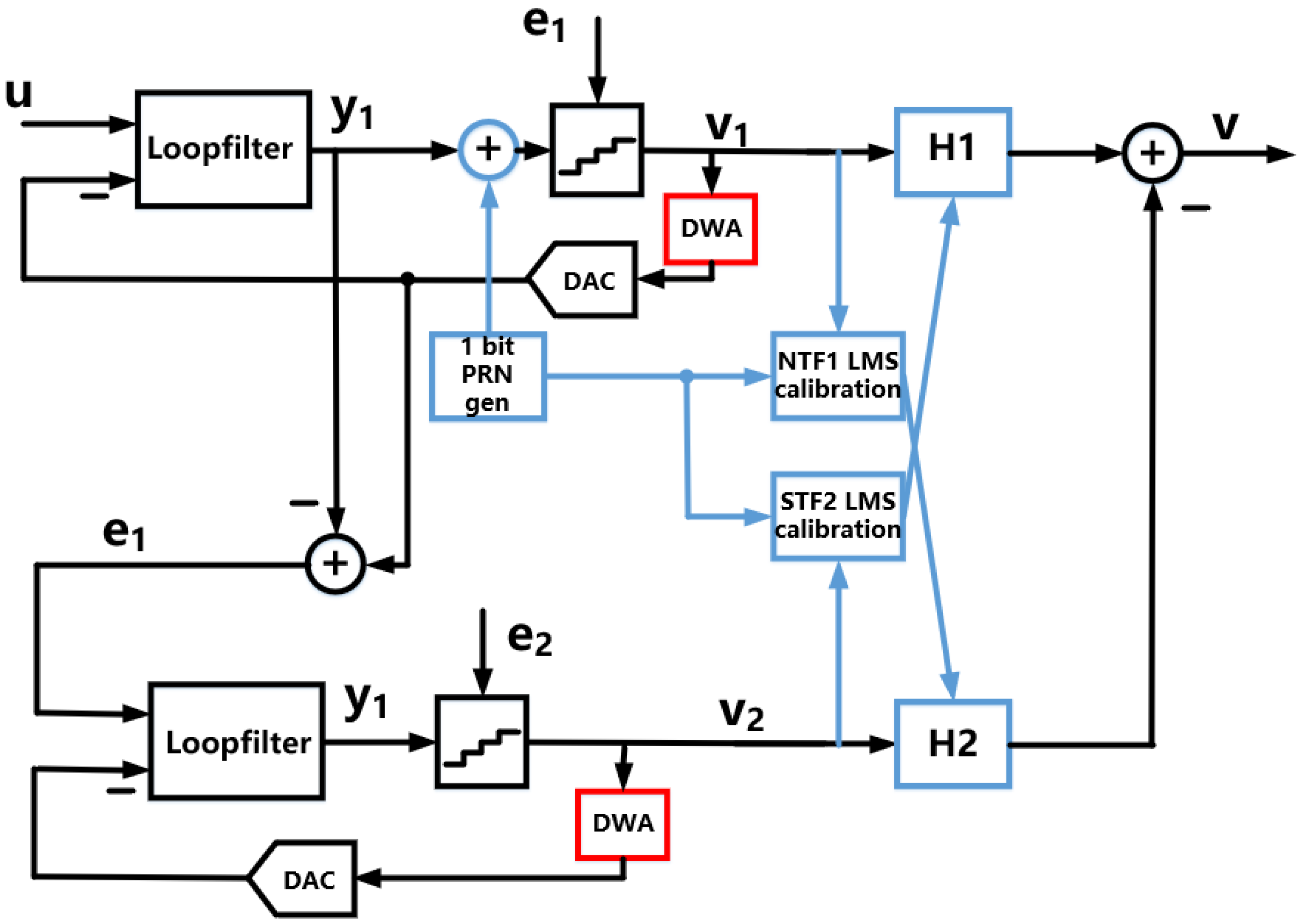
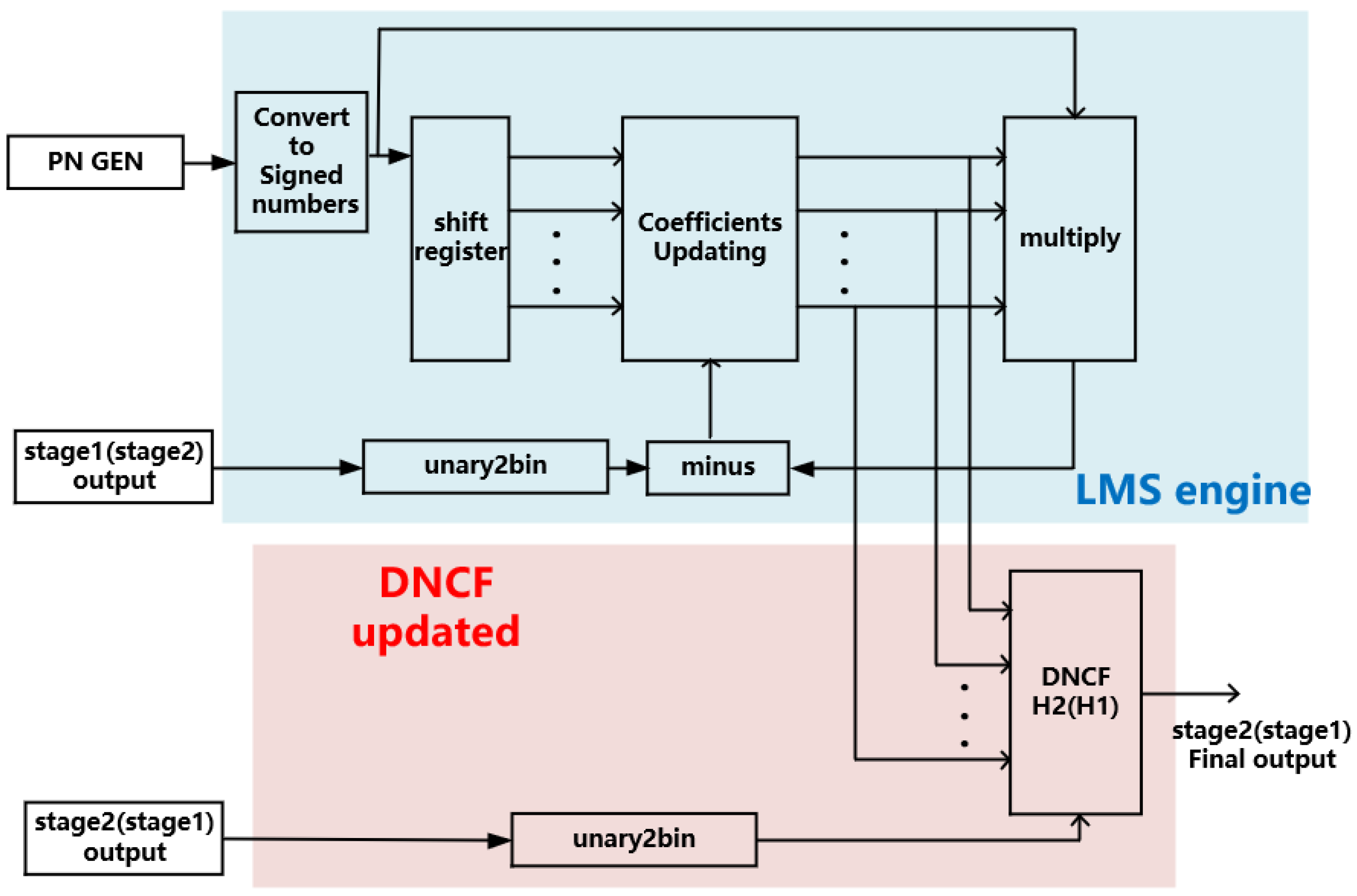
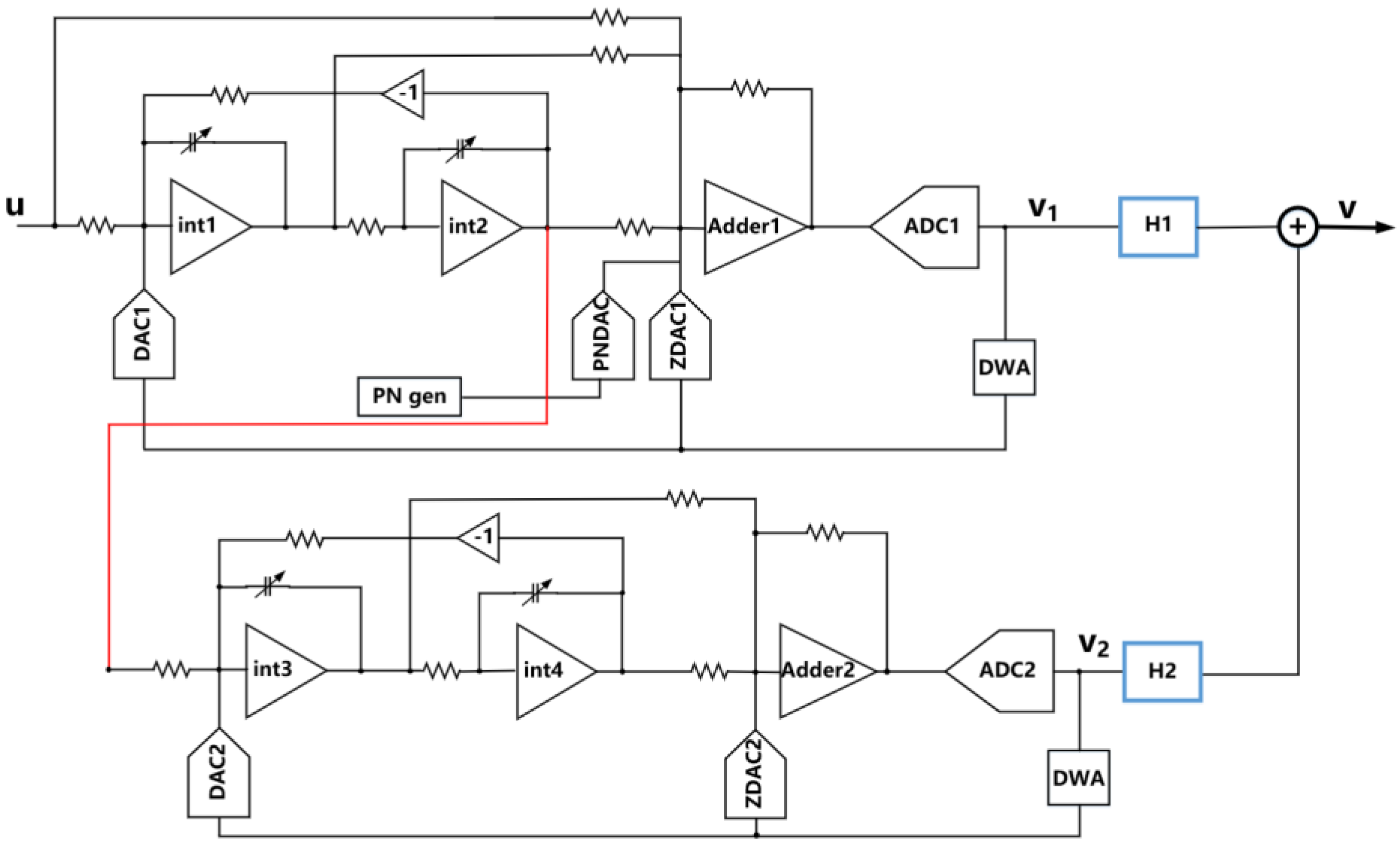
2. Proposed CT 2-2 MASH with Digital Calibration

The circuit diagram and calibration scheme proposed in this article are shown in Figure 1. The quantization noise, e 1 , of the first delta–sigma modulator (DSM) was extracted and fed into the input of the second DSM. Outputs V 1 and V 2 of the two DSMs were processed by DNCFs ( H 1 and H 1 ) and concatenated to obtain the complete output. The output expressions of the two DSMs are as follows:
V 1 s = S T F 1 s U s + N T F 1 s e 1 s
V 2 s = S T F 2 s e 1 ( s ) + N T F 2 ( s ) e 2 ( s )  
where e 1 s and e 2 s represent the quantization error of the two DSMs, S T F 1 s and S T F 2 s represent the input signal transfer functions of the two DSMs, and N T F 1 s and N T F 2 ( s ) represent the quantization noise transfer functions of the two DSMs.
The digital outputs of the two DSMs were concatenated after being processed by DNCFs to obtain the final output digital code as follows:
V s = H 1 s S T F 2 s U s + H 2 ( s ) N T F 2 ( s ) e 2 ( s ) + H 1 s N T F 1 s H 2 s S T F 2 s e 1 s  
V s = S T F 1 s S T F 2 s U s + N T F 1 ( s ) N T F 2 ( s ) e 2 ( s )      
where H 1 s and H 2 ( s ) represent the transfer functions of the two DNCFs.
It can be seen that if H 1 = S T F 2 and H 2 = N T F 1 , then e 1 will be completely eliminated, resulting in (4), which includes the input signal and the quantization noise of the second DSM after being shaped twice. However, high accuracy is required for matching the transfer functions of DNCFs with the transfer functions of an analog loop filter; otherwise, it will cause noise leakage and deteriorate the performance of the ADC.
The red part in Figure 1 is the DWA module, which is used to eliminate errors caused by DAC mismatch. The blue part is the DNCF digital calibration module, which is used to update the coefficients of the DNCF in real time to eliminate noise leakage. The DNCF calibration module includes the generation and injection of a 1-bit pseudo-random sequence (PN code), two LMS engines which are two variable coefficient FIR filters, and an upgradable Finite Impulse Response (FIR) digital filter. The position of the pseudo-random sequence injection is consistent with the quantization noise generation position of the first DSM [19].
When the pseudo-random sequence is injected, the outputs of the first-stage DSM and NTF1 LMS engine are
V 1 = S T F 1 U + N T F 1 e 1 + N T F 1 P N
Y 1 = N T F ^ 1 P N
where P N represents the pseudo-random sequence. S T F 1 and N T F 1 represent the transfer functions of the real circuits. N T F ^ 1 represents the estimated coefficient of N T F 1 .
The error items can be obtained by obtaining the difference between (5) and (6) as follows:
E = V 1 Y 1 = S T F 1 U + N T F 1 e 1 + N T F 1 N T F ^ 1 P N
After performing relevant operations between V 1 and P N , (7) becomes
E P N = S T F 1 U P N + N T F 1 e 1 P N + N T F 1 N T F ^ 1 P N P N
where represents the correlation operator. Formula (8) shows that the N T F ^ 1 closest to the actual N T F 1 can be obtained to minimize E according to the relevant characteristics of P N [25].
According to the LMS algorithm, the updating of N T F ^ 1 filter coefficients is as follows:
ω n + 1 = ω n + μ E n P N n
where ω n represents the updated coefficients of N T F ^ 1 . μ represents the iterative step size of the LMS engine.
Substituting expression (7) into Equation (9) results in the following:
ω n + 1 = ω n + μ S T F 1 U n + N T F 1 e 1 P N n + μ N T F 1 ω T n P N 2 n
Accumulating Equation (9) is equivalent to low-pass filtering, which can filter out irrelevant noise shown in the second term of (9), and the correlated term shown in the third term of (9) tends to be constant. When the algorithm converges, ω T n are the coefficients of N T F ^ 1 closest to the actual N T F 1 value.
The working principle of the STF LMS engine is the same. The coefficients of two DNCFs are updated to eliminate noise leakage. Figure 2 is a schematic diagram of the LMS algorithm, with the blue part representing this structure of the LMS engine and the red part representing the updatable DNCF. For the stability of the calibration algorithm, an 18th-order FIR filter was used as the DNCF in this design rather than an infinite impulse response (IIR) filter.
By using a behavioral-level simulation model for simulation, it was verified that digital calibration reduced the power consumption of the integrator. The simulation results are shown in Table 1. It can be seen that without digital calibration, the operational amplifier requires a DC gain of 60 dB and a gain bandwidth product of 8 GHz to ensure no noise leakage occurs. And with digital calibration, the design specifications of the operational amplifier can be relaxed to a DC gain of 40 dB and a gain bandwidth product of 4.8 GHz.

3. Circuit Implementation

The circuit of the proposed CT 2-2 MASH is shown in Figure 3, where the first stage’s loop filter is a Silva–Steensgaard structure, which facilitates the extraction of the quantization noise of the first DSM from the output of the second-stage integrator. At the same time, a local resonator was added to shift a zero point of the NTF from the zero frequency to the band edge, thereby optimizing the quantization noise within the bandwidth. The feedforward structure also allows for the output of the integrator to only contain the quantization noise component, reducing the requirement for the output swing and lowering operational amplifier power consumption. The integrators all use the active RC structure to achieve better linearity. The operational amplifiers use a two-stage feedforward compensation structure. The first DSM uses a 3-bit quantizer to reduce the quantization noise amplitude, thereby obtaining a higher OBG and more aggressive noise-shaping ability. The use of a 3-bit quantizer in the second DSM is a trade-off between the number of comparators and quantization noise. Although the quantization noise of the second-stage DSM can be shaped by the fourth-order NTF, the OBG of the second-stage DSM also needs to be considered. If the number of quantization bits is too small, a higher OBG cannot be selected, thus weakening the shaping ability of the second NTF. An active adder is used to sum all feedforward branches and the ELD compensation branch while ensuring that the loop gain is not attenuated. Among them, PNDAC is used to complete 1-bit pseudo-random sequence injection. By injecting a pseudo-random sequence at the front-end of the quantizer, the transfer function includes the gain of the quantizer, which can eliminate the impact of PNDAC mismatch [19]. The integration capacitor of each integrator is an adjustable capacitor array to correct the RC coefficient under different PVT variations.

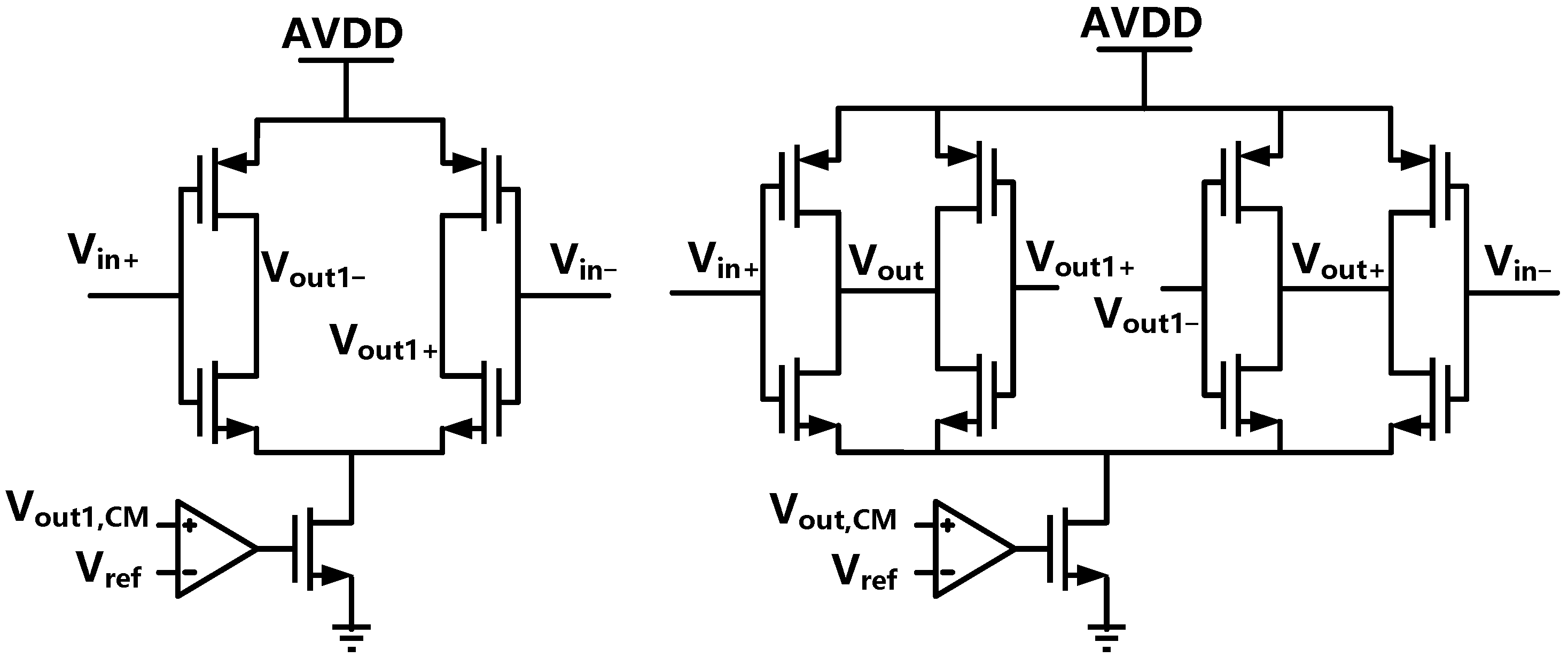
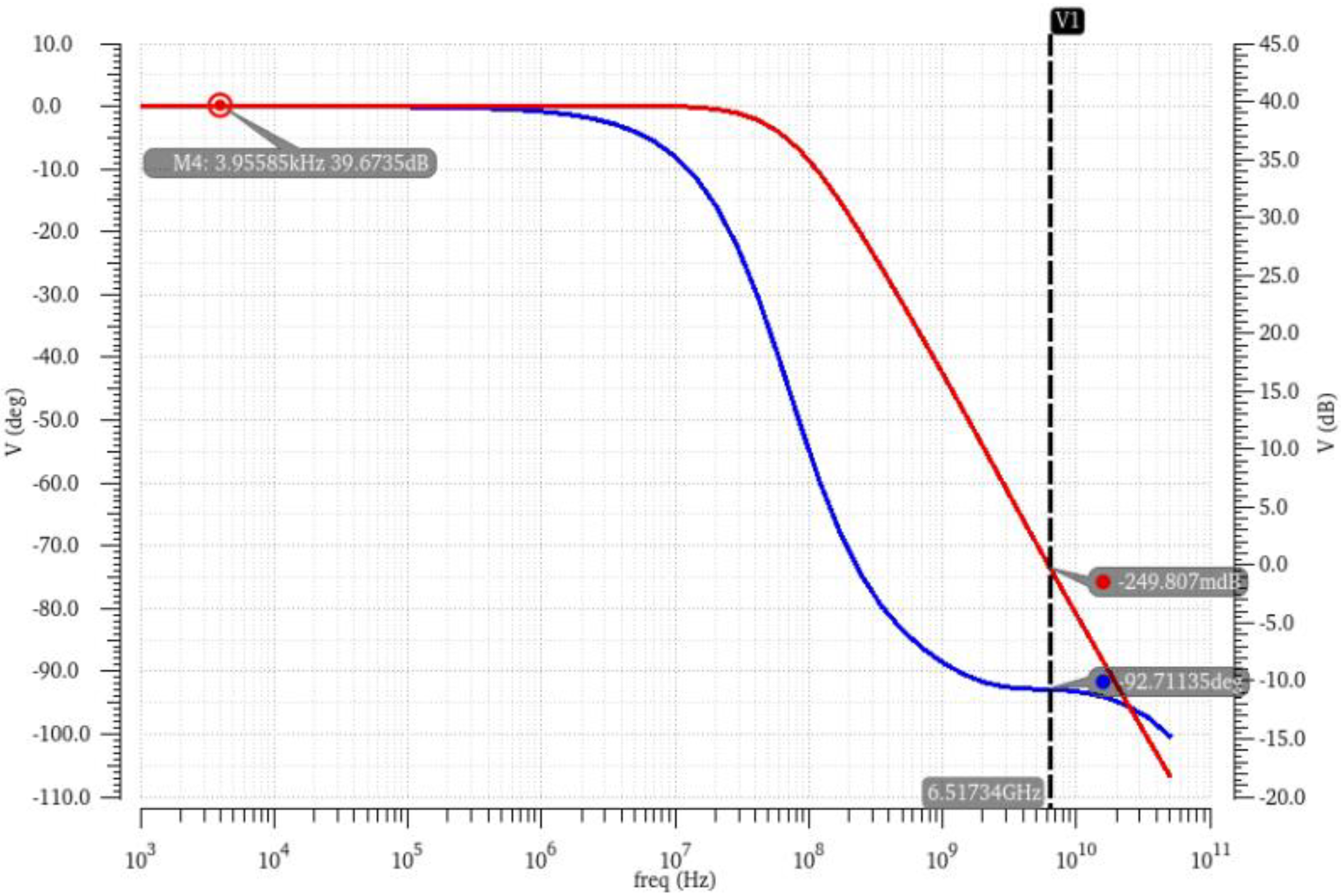
3.1. Operational Amplifier with Feedforward Compensation

The GHz sampling rate requires a high GBW for the operational amplifiers in the integrator. In order to provide sufficient gain with small channel lengths, a multi-stage operational amplifier is needed. This design uses two-stage operational amplifiers and ensures stability using feedforward compensation, as shown in Figure 4. Compared to Miller compensation, feedforward compensation does not require an additional capacitor load for the second stage, thus saving power consumption with the same bandwidth and phase margin [26]. The complementary input pairs can improve transconductance under a certain current [27]. Taking the first integrator operational amplifier as an example, this structure can achieve a DC gain of 39.7 dB and a UGB of 6.5 GHz with a power consumption of 4.19 mW. The frequency response curve of the first operational amplifier is shown in Figure 5.

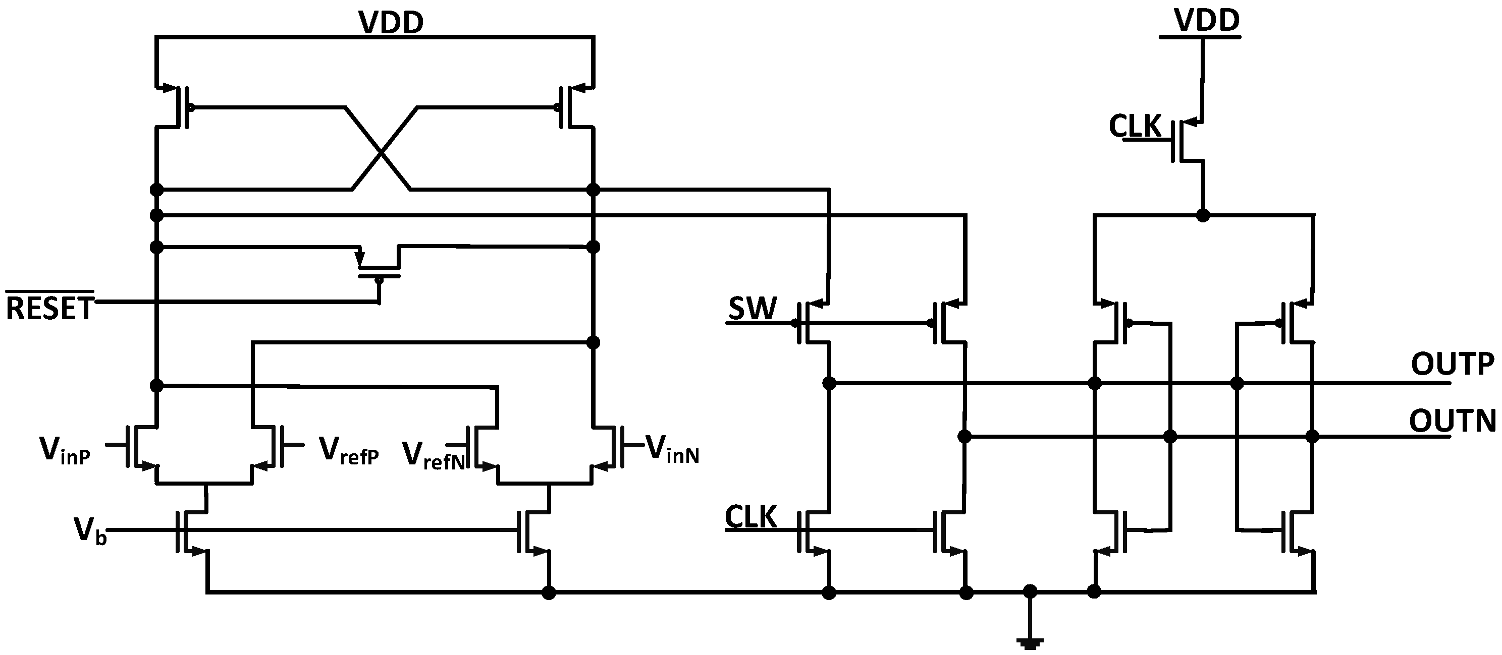
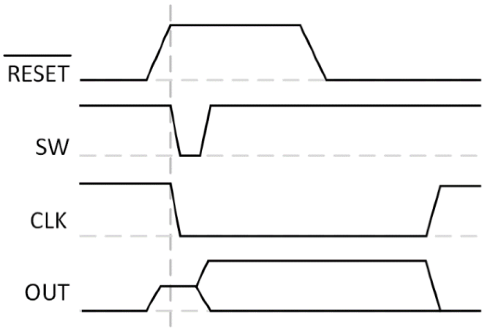
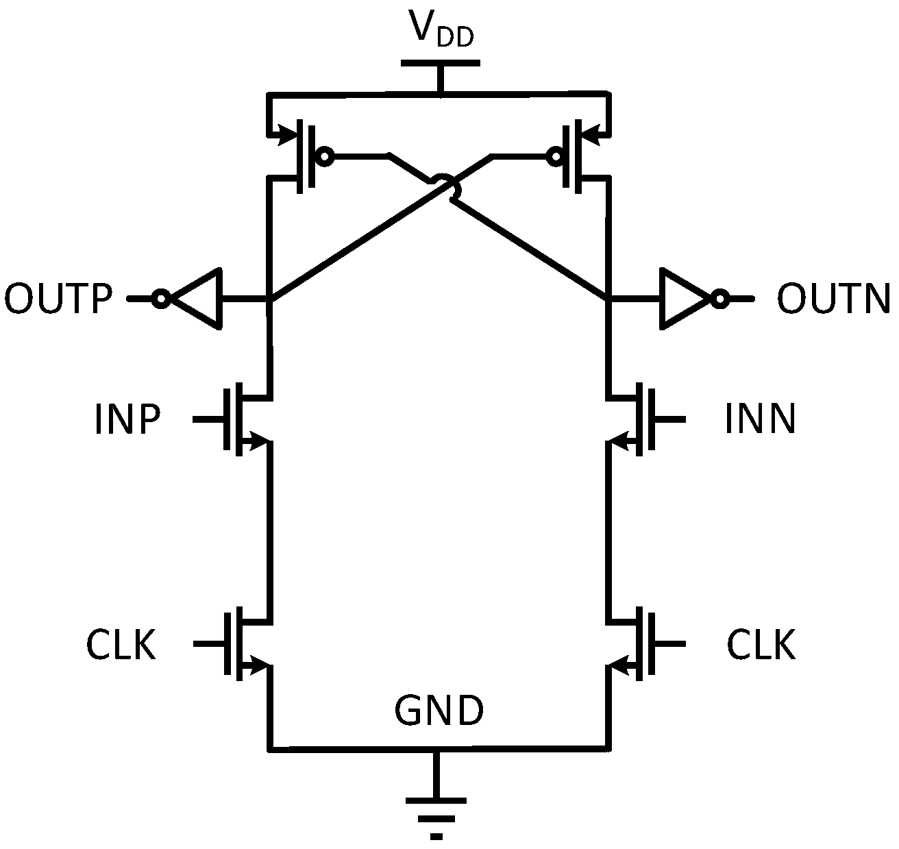
3.2. Flash Quantizer and Comparator

Considering the 1.6 GHz clock frequency and quantization bit count of no more than 4 bits, the quantizer uses a flash ADC for faster speed. The comparator structure is shown in Figure 6 [28]. When the reset signal is 0, the comparator is reset. When the reset signal is 1, the current generated from the input transistor creates a voltage difference across the cross-coupled load transistor.
Immediately thereafter, the switch, SW, is turned on, and the output latch is activated. The output latch has a very small time constant and amplifies small voltage differences to logic levels. To reduce the impact of kickback noise, the switch, SW, disconnects the signal path from the preamplifier to the latch before the latch output voltage reaches a high level, as shown in the timing diagram in Figure 7.

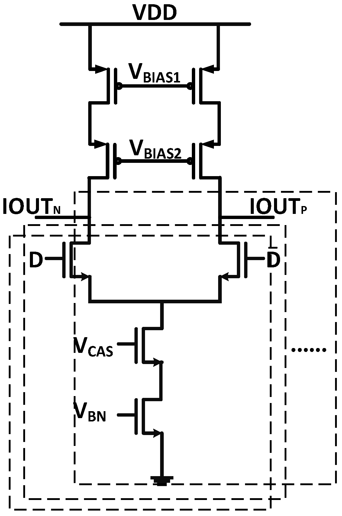
3.3. Current Steering DAC

Feedback DAC is one of the most critical modules in CTSD ADC as it directly outputs to the front-end of the DSM, and any nonidealities will not be shaped. The commonly used types of feedback DAC include switch capacitor DAC, switch resistor DAC, and current steering DAC. Among them, current steering DAC has the fastest establishment speed, does not load the virtual ground node of the integrator, and does not damage anti-aliasing characteristics. Therefore, it is most commonly used in high-speed CTSD ADCs. The circuit schematic of this design is shown in Figure 8. The PMOS cascode current mirror above serves as a common-mode current source, while the NMOS cascode current mirror below serves as a DAC unit controlled by the digital code of the quantizer.
There is a synchronous latch in front of each DAC unit to ensure that the digital signal arrives at the same time. The driving circuit should also achieve the function of a high crossing point to avoid the spike caused by the simultaneous closure of two switch transistors of the NMOS current source. The high-speed latch used in this design is shown in Figure 9, where the stacked NMOS switches are controlled by clock and data signals. The introduction of positive feedback in cross-coupled PMOS transistors allows for the output node’s voltage level to have steep rising and falling edges. By adjusting the size of the transistor, a suitable high crossing point can be obtained. The smaller the energy of the switching spike, the smaller the harmonic distortion caused by DAC switching.
The mismatch current of the current steering DAC cell is simulated 200 times by Monte Carlo, and the simulation results are shown in Figure 10.

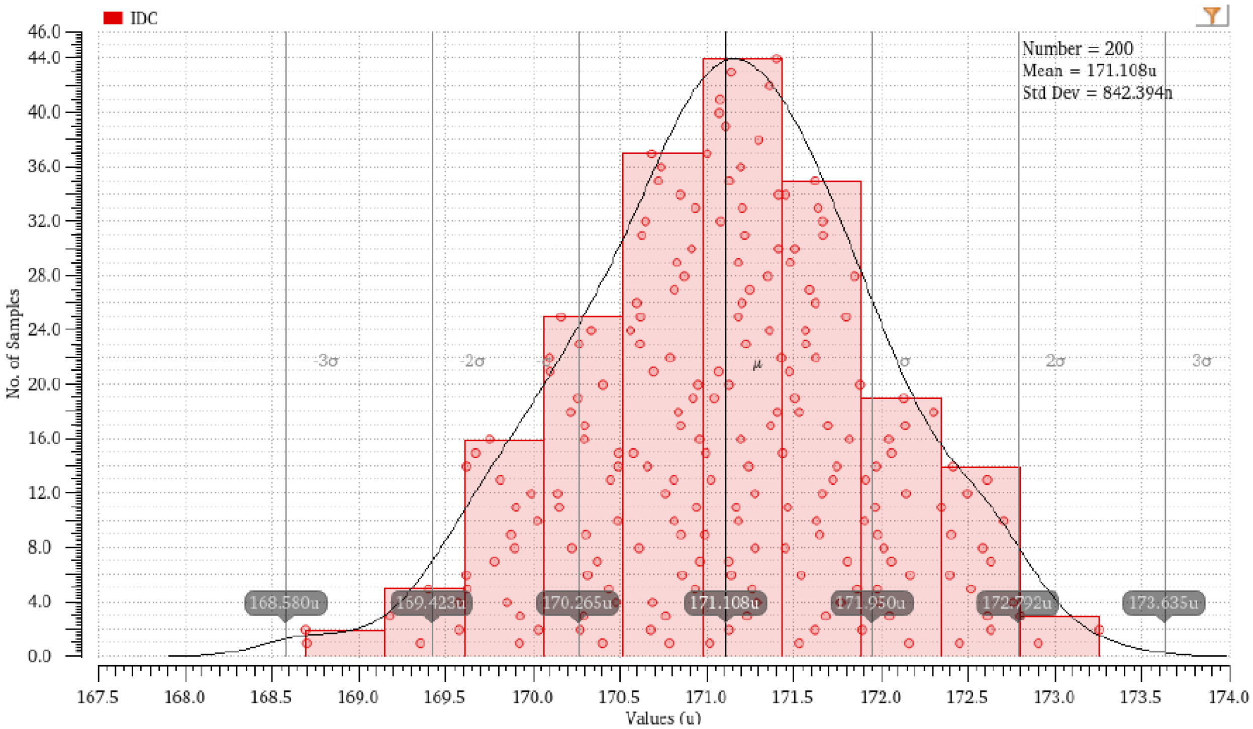
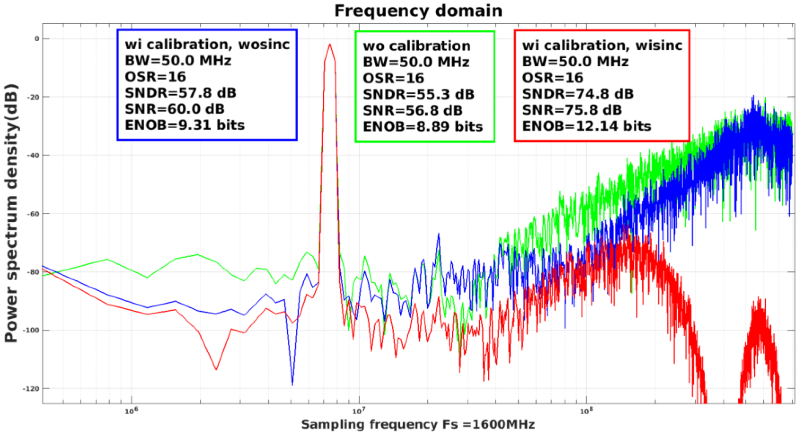
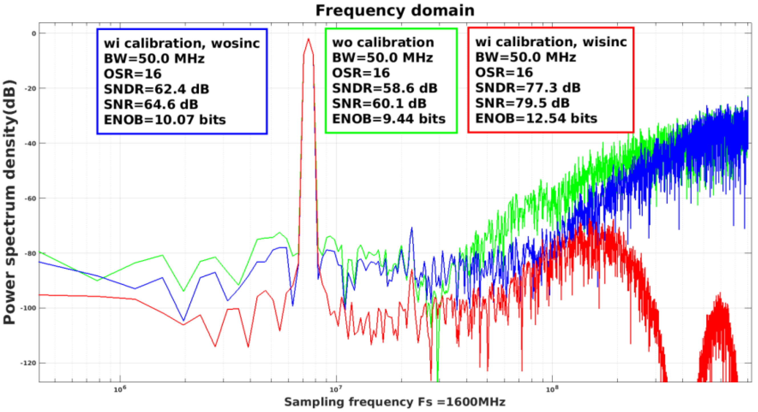
4. Simulation Results and Discussion

The presented CT 2-2 MASH ADC was designed and simulated in 40 nm CMOS with 1.2 V/0.9 V supply voltages. The digital calibration of a DNCF was validated on ZYNQ-7020, as shown in Figure 11.
This calibration algorithm uses limited resources in FPGA, as shown in Table 2. The Processing System (PS) loads the data from Virtuoso stored in the SD card, including the PN code and the output digital codes of the two stages. The Programmable Logic (PL) implements the hardware circuit for the LMS algorithm and DNCF.
Figure 12 shows the transistor-level simulated PSD of the presented ADC with 4096 sampling points, where transient noise is included. The green spectrum shows the uncalibrated result. It can be seen that because the DNCFs do not match the STF and NTF, noise leakage occurred, resulting in a SNR of only 57.6 dB. The blue spectrum is the calibration result obtained by directly searching the transfer function, and the calibration effect is very poor, resulting in a SNR of only 61.4 dB. From the spectrum perspective, although the characteristic of fourth-order noise shaping is also reflected at high frequencies, it can be seen that there is a tendency for the spectrum to rise within the bandwidth, and noise cancelation is not good. This is because the parasitic pole at the input of the quantizer causes the NTF peaking. This peak will have a serious impact on the convergence process of various coefficients in the LMS engine, requiring more taps and calibration points to complete sufficient convergence. Therefore, it is necessary to use a digital low-pass filter to eliminate NTF peaking before calibration. The final calibration result after filtering using an FIR low-pass filter is shown as the red spectrum in Figure 12, achieving a SNDR of 76.8 dB and a SNR of 78.3 dB.
Figure 13 shows the MASH calibration effect, achieving a SNDR of 74.8 dB under the simulation condition of the SS process corner and 100 °C, and Figure 14 shows the MASH calibration effect, achieving a SNDR of 77.3 dB under the simulation condition of the ff process corner and −40 °C.
The power consumption of the entire CT 2-2 MASH is 29.7 mW, with DAC and the operational amplifier occupying the main parts because these two components are the main source of thermal noise. A power distribution diagram is shown in Figure 15. The ADC performance is summarized and compared with state-of-the-art designs in Table 3.
The simulation results show that the CT 2-2 MASH ADC proposed in this paper achieves competitive SNDR and SFDR values after calibration. Compared with [22], the use of digital calibration instead of low-precision analog calibration reduces power consumption even at a higher clock frequency. Compared with [19], this paper removes the complex SAR logic embedded with ELD compensation and achieves a higher bandwidth using the same MASH calibration. The advantages of the MASH structure in broadband application were fully demonstrated in ref. [24], but the accuracy was lower than the proposed MASH ADC. In [12], due to the noise shaping order being lower than that of the proposed MASH ADC, a higher OSR was used, resulting in excessive power consumption. Although the work presented in this article is based on simulation results, it confirms that the selected circuit architecture and digital calibration scheme have certain advantages.

5. Conclusions

In this article, a CT 2-2 MASH ADC with digital calibration is proposed. The loop filter adopts the Silva-Steensgaard structure, which facilitates the extraction of the quantization error of the first stage while reducing the power consumption of the integrator. A two-stage feedforward compensation operational amplifier with complementary input pairs was adopted to reduce power consumption while ensuring high GBW. The mismatch error of DAC was eliminated by DWA. The coefficients of the DNCF were calibrated using the LMS algorithm to suppress noise leakage. Simulated in 40 nm CMOS, the proposed MASH ADC achieved a 76.8 dB SNDR and 50 MHz bandwidth with a 1.6 GHz sampling clock. The modulator consumes about 29.7 mW of power, with a competitive figure of merit (FoM) of 169.1 dB. And the calibration algorithm was run on a FPGA.

Author Contributions

Research methodology, X.S.; circuit design, X.S.; calibration algorithm design, X.S. and Z.L.; writing—original draft preparation, Z.L.; supervision, X.X. and H.F. All authors have read and agreed to the published version of the manuscript.

Funding

This work was supported and funded in part by the Guangdong Key Area Research and Development Program, China (2019B010143003); the Shenzhen Science and Technology innovative committee, China (GJHZ20200731095609029); and the Natural Science Foundation of Guangdong Province, China (Grant No. 2024A1515010997).

Institutional Review Board Statement

Not applicable.

Informed Consent Statement

Not applicable.

Data Availability Statement

The original contributions presented in this study are included in the article. The data presented in this study are available in this paper.

Conflicts of Interest

The authors declare no conflicts of interest.

References

  1. Loeda, S.; Harrison, J.; Pourchet, F.; Adams, A. A 10/20/30/40 MHz feedforward FIR DAC continuous-time ∆Σ ADC with robust blocker performance for radio receivers. IEEE J. Solid State Circuits 2016, 51, 860–870. [Google Scholar]
  2. de la Rosa, J.M.; Schreier, R.; Pun, K.-P.; Pavan, S. Next-Generation Delta-Sigma Converters: Trends and Perspectives. IEEE J. Emerg. Sel. Top. Circuits Syst. 2015, 5, 484–499. [Google Scholar] [CrossRef]
  3. Xing, K.; Wang, W.; Zhu, Y.; Chan, C.-H.; Martins, R.P. A Single-Opamp Third Order CT ΔΣ Modulator with SAB-ELD-Merged Integrator and Three-Stage Hybrid Compensation Opamp. IEEE Trans. Circuits Syst. I Regul. Pap. 2022, 69, 64–74. [Google Scholar] [CrossRef]
  4. Breems, L.J.; Bolatkale, M.; Liu, Q.; Cenci, P. High-Speed and High-Performance Continuous-Time ADCs for Automotive Re-ceivers. IEEE Open J. Solid-State Circuits Soc. 2023, 3, 174–184. [Google Scholar] [CrossRef]
  5. Ucar, A.; Cetin, E.; Kale, I. A Continuous-Time Delta-Sigma Modulator for RF Subsampling Receivers. IEEE Trans. Circuits Syst. II Express Briefs 2012, 59, 272–276. [Google Scholar] [CrossRef]
  6. Lai, W.-C. Continuous-time Sigma-Delta Modulator with RF Receiver for Wireless Respiratory Detection. In Proceedings of the 2021 IEEE International Symposium on Radio-Frequency Integration Technology (RFIT), Hualien, Taiwan, 25–27 August 2021; pp. 1–3. [Google Scholar]
  7. Wang, C.-Y.; Tsai, J.-H.; Su, S.-Y.; Tsai, J.-C.; Chen, J.-R.; Lou, C.-H. 20.6 An 80MHz-BW 31.9fJ/conv-step Filtering ΔΣ ADC with a Built-In DAC-Segmentation/ELD-Compensation 6b 960MS/s SAR-Quantizer in 28 nm LP for 802.11ax Applications. In Proceedings of the 2019 IEEE International Solid—State Circuits Conference—(ISSCC), San Francisco, CA, USA, 17–21 February 2019; pp. 338–340. [Google Scholar]
  8. Shibata, H.; Kozlov, V.; Ji, Z.; Ganesan, A.; Zhu, H.; Paterson, D.; Pavan, S. A 9-GS/s 1.125-GHz BW Oversampling Continuous-Time Pipeline ADC Achieving −164-dBFS/Hz NSD. IEEE J. Solid-State Circuits 2017, 52, 3219–3234. [Google Scholar] [CrossRef]
  9. Caldwell, T.; Shibata, H. High-speed oversampled continuous-time analog-to-digital converters. In Proceedings of the 2017 IEEE 60th International Midwest Symposium on Circuits and Systems (MWSCAS), Boston, MA, USA, 6–9 August 2017; pp. 1001–1004. [Google Scholar]
  10. Bolatkale, M.; Breems, L.J.; Rutten, R.; Makinwa, K.A.A. A 4 GHz Continuous-Time ΔΣ ADC with 70 dB DR and—74 dBFS THD in 125 MHz BW. IEEE J. Solid State Circuits 2011, 46, 2857–2868. [Google Scholar] [CrossRef]
  11. Park, M.; Perrott, M.H. A 78 dB SNDR 87 mW 20 MHz Bandwidth Continuous-Time ΔΣ ADC with VCO-Based Integrator and Quantizer Implemented in 0.13 μm CMOS. IEEE J. Solid State Circuits 2009, 44, 3344–3358. [Google Scholar] [CrossRef]
  12. Mukherjee, A.; Gandara, M.; Yang, X.; Shen, L.; Tang, X.; Hsu, C.K.; Sun, N. A 74.5-dB Dynamic Range 10-MHz BW CT-ΔΣ ADC with Distributed-Input VCO and Embedded Capacitive-π Network in 40-nm CMOS. IEEE J. Solid State Circuits 2021, 56, 476–487. [Google Scholar] [CrossRef]
  13. Huang, S.-J.; Egan, N.; Kesharwani, D.; Opteynde, F.; Ashburn, M. 28.3 A 125MHz-BW 71.9dB-SNDR VCO-based CT ΔΣ ADC with segmented phase-domain ELD compensation in 16nm CMOS. In Proceedings of the 2017 IEEE International Solid-State Circuits Conference (ISSCC), San Francisco, CA, USA, 5–9 February 2017; pp. 470–471. [Google Scholar]
  14. Taylor, G.; Galton, I. A Mostly-Digital Variable-Rate Continuous-Time Delta-Sigma Modulator ADC. IEEE J. Solid State Circuits 2010, 45, 2634–2646. [Google Scholar] [CrossRef]
  15. Dong, Y.; Yang, W.; Schreier, R.; Sheikholeslami, A.; Korrapati, S. A Continuous-Time 0–3 MASH ADC Achieving 88 dB DR with 53 MHz BW in 28 nm CMOS. IEEE J. Solid State Circuits 2014, 49, 2868–2877. [Google Scholar] [CrossRef]
  16. Dong, Y.; Zhao, J.; Yang, W.W.; Caldwell, T.; Shibata, H.; Li, Z.; Gealow, J.C. A 72 dB-DR 465 MHz-BW Continuous-Time 1–2 MASH ADC in 28 nm CMOS. IEEE J. Solid State Circuits 2016, 51, 2917–2927. [Google Scholar] [CrossRef]
  17. Zhang, J.Z.; Steensgaard, G.; Temes, C.; Wu, J.-Y. A Split 2-0 MASH with Dual Digital Error Correction. In Proceedings of the 2007 IEEE Symposium on VLSI Circuits, Kyoto, Japan, 14–16 June 2007; pp. 242–243. [Google Scholar] [CrossRef]
  18. Shu, Y.-S.; Kamiishi, J.; Tomioka, K.; Hamashita, K.; Song, B.-S. LMS-Based Noise Leakage Calibration of Cascaded Continuous-Time ΔΣ Modulators. IEEE J. Solid-State Circuits 2010, 45, 368–379. [Google Scholar] [CrossRef]
  19. Fukazawa, M.; Oshima, T.; Fujiwara, M.; Tateyama, K.; Ochi, A.; Alsubaie, R.; Matsui, T. A CT 2–2 MASH ΔΣ ADC with Multi-Rate LMS-Based Background Calibration and Input-Insensitive Quantization-Error Extraction. IEEE J. Solid State Circuits 2021, 56, 2943–2955. [Google Scholar] [CrossRef]
  20. Fukazawa, M.; Oshima, T.; Fujiwara, M.; Tateyama, K.; Raed, A.; Ito, M.; Matsui, T. 9.7 Background Multi-Rate LMS Calibration Circuit for 15MHz-BW 74dB-DR CT 2–2 MASH ΔΣ ADC in 28nm CMOS. In Proceedings of the 2020 IEEE International Solid-State Circuits Conference—(ISSCC), San Francisco, CA, USA, 16–20 February 2020; pp. 166–168. [Google Scholar]
  21. Yoon, D.-Y.; Ho, S.; Lee, H.-S. A Continuous-Time Sturdy-MASH ΔΣ Modulator in 28 nm CMOS. IEEE J. Solid State Circuits 2015, 50, 2880–2890. [Google Scholar] [CrossRef]
  22. Qi, L.; Jain, A.; Jiang, D.; Sin, S.-W.; Martins, R.P.; Ortmanns, M. A 76.6-dB-SNDR 50-MHz-BW 29.2-mW Multi-Bit CT Sturdy MASH with DAC Non-Linearity Tolerance. IEEE J. Solid State Circuits 2020, 55, 344–355. [Google Scholar] [CrossRef]
  23. Park, B.; Han, C.; Maghari, N. Correlated Dual-Loop Sturdy MASH CT ΔΣ ADC with Indirect Signal Feedforward. In Proceedings of the 2021 IEEE Asian Solid-State Circuits Conference (A-SSCC), Busan, Republic of Korea, 7–10 November 2021; pp. 1–3. [Google Scholar]
  24. Han, C.; Park, B.; Maghari, N. Can SMASH Smash MASH? In Proceedings of the 2018 IEEE International Symposium on Circuits and Systems (ISCAS), Florence, Italy, 27–30 May 2018; pp. 1–5. [Google Scholar]
  25. Ali, A.M.; Dinc, H.; Bhoraskar, P.; Dillon, C.; Puckett, S.; Gray, B.; McShea, M. A 14 Bit 1 GS/s RF Sampling Pipelined ADC with Background Calibration. IEEE J. Solid State Circuits 2014, 49, 2857–2867. [Google Scholar] [CrossRef]
  26. Ho, S.; Lo, C.-L.; Ru, J.; Zhao, J. A 23 mW, 73 dB Dynamic Range, 80 MHz BW Continuous-Time Delta-Sigma Modulator in 20 nm CMOS. IEEE J. Solid State Circuits 2015, 50, 908–919. [Google Scholar] [CrossRef]
  27. Liu, H.; Xing, X.; Gielen, G. A 0-dB STF-Peaking 85-MHz BW 74.4-dB SNDR CT ΔΣ ADC with Unary-Approximating DAC Calibration in 28-nm CMOS. IEEE J. Solid State Circuits 2021, 56, 287–297. [Google Scholar] [CrossRef]
  28. Mitteregger, G.; Ebner, C.; Mechnig, S.; Blon, T.; Holuigue, C.; Romani, E. A 20-mW 640-MHz CMOS Continuous-Time ΣΔ ADC with 20-MHz Signal Bandwidth, 80-dB Dynamic Range and 12-bit ENOB. IEEE J. Solid State Circuits 2006, 41, 2641–2649. [Google Scholar] [CrossRef]
  29. Edward, A.; Liu, Q.; Briseno-Vidrios, C.; Kinyua, M.; Soenen, G.E.; Karsilayan, I.A. A 43-mW MASH 2-2 CT ΣΔ Modulator Attaining 74.4/75.8/76.8 dB of SNDR/SNR/DR and 50 MHz of BW in 40-nm CMOS. IEEE J. Solid State Circuits 2017, 52, 448–459. [Google Scholar] [CrossRef]
  30. Honarparvar, M.; de la Rosa, J.M.; Sawan, M. A 10-MHz BW 77.3-dB SNDR 640-MS/s GRO-Based CT MASH ΔΣ Modulator. IEEE Trans. Circuits Syst. II Express Briefs 2020, 67, 1519–1523. [Google Scholar]
  31. Liu, Q.; Breems, L.J.; Bajoria, S.; Bolatkale, M.; Rutten, R.; Radulov, G. A 158-mW 360-MHz BW 68-dB DR Continuous-Time 1-1-1 Filtering MASH ADC in 40-nm CMOS. IEEE J. Solid State Circuits 2022, 57, 3781–3793. [Google Scholar] [CrossRef]
Figure 1. Circuit and calibration diagram of proposed CT 2-2 MASH.
Jlpea 15 00020 g001
Figure 2. LMS algorithm implementation diagram in FPGA.
Jlpea 15 00020 g002
Figure 3. Overall schematic of proposed CT 2-2 MASH.
Jlpea 15 00020 g003
Figure 4. Two-stage feedforward compensation operational amplifier.
Jlpea 15 00020 g004
Figure 5. The frequency response of the operational amplifier in the first integrator.
Jlpea 15 00020 g005
Figure 6. Circuit implementation of two-stage comparator.
Jlpea 15 00020 g006
Figure 7. Timing diagram of comparator.
Jlpea 15 00020 g007
Figure 8. Circuit implementation of current steering DAC.
Jlpea 15 00020 g008
Figure 9. Circuit implementation of high-speed latch.
Jlpea 15 00020 g009
Figure 10. Monte Carlo simulation of current steering DAC mismatch.
Jlpea 15 00020 g010
Figure 11. FPGA verification platform.
Jlpea 15 00020 g011
Figure 12. Simulated spectrum with/without calibration at tt process corner, 27 °C.
Jlpea 15 00020 g012
Figure 13. Simulated spectrum with/without calibration at ss process corner, 100 °C.
Jlpea 15 00020 g013
Figure 14. Simulated spectrum with/without calibration at ff process corner, -40 °C.
Jlpea 15 00020 g014
Figure 15. Power distribution.
Jlpea 15 00020 g015
Table 1. Comparison of calibration performance of different operational amplifiers.
Opamp 1-1 A D C   ( dB ) ,
GBW (Hz)
Opamp 1-2 A D C   ( dB ) ,
GBW (Hz)
Opamp 2-1 A D C   ( dB ) ,
GBW (Hz)
Opamp 2-2 A D C   ( dB ) ,
GBW (Hz)
Wo Calibration
ENOB
(bit)
Foreground Calibration
ENOB
(bit)
Background Calibration
ENOB
(bit)
160,
8 G
60,
8 G
60,
8 G
60,
8 G
14.1813.9014.05
240,
4.8 G
40,
4.8 G
40,
4.8 G
40,
4.8 G
12.5414.3313.87
334,
3.2 G
34,
3.2 G
34,
3.2 G
34,
3.2 G
11.7614.0813.25
430,
1.6 G
30,
1.6 G
30,
1.6 G
30,
1.6 G
10.7513.5012.78
Table 2. Digital calibration resources in FPGA.
CharacteristicThis Work
FamilyZynq-7020
Devicexc7z020clg400-2
Number of LUTs13,512/53,200 (25.4%)
Number of registers3753/106,400 (3.5%)
Frequency50 M
Number of sampling
points required
2 × 10 5
Table 3. A performance summary and comparison with state-of-the-art designs.
This Work *[12][18][29][30][31]
ArchitectureMASH 2-2MASH 0-3SMASH 3-1MASH 2-2MASH 3-1MASH 1-1-1
Process (nm)402828406540
Supply (V)1.2/0.91.8/0.9/−1.01.2/1.51.1/1.15/2.51.01.8/1.1/1
BW (Hz)50 M53 M50 M50 M10 M360 M
Fs (Hz)1.6 G3.2 G1.8 G1.0 G0.64 G5 G
SNDR (dB)76.871.474.974.477.365
SNR (dB)78.383.176.875.879.865
Power (mW)29.723580.443.012158
FOMs (dB) **169.1155162.8165.1167.8159
* Simulation results. ** F O M s = S N D R + 10 l o g B W P o w e r .
Disclaimer/Publisher’s Note: The statements, opinions and data contained in all publications are solely those of the individual author(s) and contributor(s) and not of MDPI and/or the editor(s). MDPI and/or the editor(s) disclaim responsibility for any injury to people or property resulting from any ideas, methods, instructions or products referred to in the content.

