1. Introduction
Low-power applications that require a certain amount of security such as passive Radio Frequency IDentification (RFID) and smart cards feature loose constraints in terms of speed performance, but are highly challenging in terms of power consumption and chip area [
1,
2,
3,
4,
5]. Hence, to reduce the power consumption, designers either reduce the power supply or the operating frequency or both. For example, in passive RFID tags, the operating frequency of the digital blocks can be as low as 100 kHz [
6]. For smart cards, the operating frequency is in the MHz range, for example in contactless smart cards such as [
4,
7], the clock frequency is 13.56 MHz compliant with the ISO/IEC 14443 standard [
8]. Another important aspect of such applications is the security level of the implementation [
6,
9,
10]. To obtain a secure chip, a combination of light-weight low-power secure protocol, algorithm and hardware should be implemented.
Currently, static CMOS logic is widely used in digital circuit design for low-power (LP) applications due to its inherent low power, small size (compared to dynamic differential logic styles (DDL)), robustness to voltage scaling and scalability with technology. It is also highly automated in CAD tools which makes it an ideal choice for logic functions. However for secure applications, static CMOS logic is not suitable, since its dynamic power consumption is highly correlated to the processed data. Such a deficiency leads to leaking information about the secured data through analyzing the instantaneous power consumption. Resulting deciphering is called power-analysis (PA) attacks [
11]. There exist many solutions (protocol-level, e.g., [
12], algorithm-level, e.g., [
13], implementation-level, e.g., [
14]) which allows improving security against such attacks. However, these solutions cause significant performance degradations. An important research goal is to determine the best security
versus performance tradeoff. In this paper we consider implementation-level solutions, in particular DDL styles that are intuitively attractive as they tackle the problem directly where it lies.
Several logic styles are proposed in the literature, such as sense amplifier based logic (SABL) [
14], wave dynamic differential logic (WDDL) [
15], charge-recycling SABL [
16], dynamic current mode logic (DyCML) [
17], MOS current-mode logic (MCML) [
18] and dynamic differential swing-limited logic (DDSLL) [
19]. Most of these logic styles share the fact that they are dynamic and differential. Indeed, as explained in [
14], a DDL style is crucial to hide, to a first order, information about the processed data. Yet, the implementation of complex logic functions causes asymmetries in the gate if care is not taken during the design phase [
14]. These asymmetries are the result of unbalanced intrinsic differential output capacitances.
Unfortunately, previous work have shown that such solutions were much less efficient than static CMOS, making them unattractive for low-cost, low-power applications. For example, implementing an SABL Kasumi S-box results in an area increase by a factor of 1.8× and an increase in energy per cycle by a factor of 2× compared to static CMOS using a 0.18
µm 1.8 V CMOS technology [
14]. WDDL style [
15] is another example where the implementation of a WDDL AES coprocessor in 0.18
µm
1.8 V CMOS technology costs a 3× increase in area and a 3.7× increase in power consumption at 50 MHz, also compared to static CMOS [
20]. It is worth mentioning that both SABL and WDDL are full-custom full-swing styles. On the other hand, DyCML [
17] which is a low-swing, self-timed logic, shows 18% less power consumption compared to static CMOS using the Khazad S-box as a test case and implemented using 0.13
µm 1.2 V CMOS partially depleted (PD) SOI technology [
21]. Although MCML is not a DDL style, it is a strong candidate for secure applications [
18,
22,
23]. However, its main drawbacks are the area increase which can reach a factor of 2 compared to static CMOS and the power consumption increase at low frequencies. Again, it is a semi-custom low-swing logic.
On the other hand, DDSLL [
19] is an interesting option as simulation results of a Khazad S-box using
µm 1.2 V CMOS PD SOI technology show that DDSLL consumes comparable power to that of DyCML while having a reduction in delay ranging from a factor of 2.2–5.2, depending on the output swing of the DyCML [
19]. Consequently, we investigate the performance of DDSLL style with the aim to:
have performances (speed and power) in the range of standard CMOS, with significant security improvement,
achieve a security level similar to previously introduced DDL styles, with significant perfor- mance improvement.
With CMOS scaling, another important aspect is to consider the increasing process variations. Variability is thought to improve the security performance of static CMOS logic against PA attacks as it makes a successful attack more difficult [
24]. In this paper we address, for the first time to the authors’ knowledge, the effect of variability on the power consumption of the DDSLL style and compare it to the static CMOS for the sake of the completeness of the research. Indeed, static CMOS is well known for its vulnerability to variability as its delay and leakage power are deeply affected by process variations specially in the subthreshold regime [
25,
26,
27]. In addition, another new impact of process variations on static CMOS, which appears in sub 65 nm CMOS technology, is the variability of the dynamic power [
28]. This might jeopardize power closure (supply rail sizing, decap insertion, regulator design) in wireless secure applications such as RFIDs which are highly power- and cost-constrained. Dynamic power variability is thus another pitfall of static CMOS for these types of applications. In this context, this paper extends the study of the effect of variability on the dynamic energy of static CMOS logic and offers a solution by adopting the DDSLL as a glitch-free style having a deterministic
αF which results in a constant, glitch-independent variability.
Generally, variability can be classified either:
spatially as within-die (WID), die-to-die (D2D), wafer-to-wafer (W2W) and lot-to-lot (L2L) [
26,
29].
or according to their nature as random (due to random dopant fluctuation (RDF), line edge roughness (LER),
etc.) , environmental (such as supply and temperature variations) and systematic (for example well proximity effects and wire thickness variation) [
26].
In this paper we consider two different types of variability, namely WID variability which incorporates uncorrelated random variations that affect each transistor independently and D2D variability of the systematic nature that affects all transistors on a die in the same way. Environmental variations are beyond the scope of this paper.
Consequently, this paper extends the work of Hassoune
et al. [
19] on the DDSLL style to further design details and optimizations. Also, a thorough analysis is conducted to compare the performance of the DDSLL style in terms of power and delay to that of the static CMOS using a more advanced technology node than the one in [
19], namely the 65 nm LP technology which is not far from being used in RFID and smart cards. In addition, to enhance the power-area efficiency, a new technique is adopted to share the redundant blocks of the DDSLL style. As for the security analysis against PA attacks, we illustrate, using the perceived information metric [
30], that security of the DDSLL style is indeed significantly improved with respect to the static CMOS and other DDL styles. Furthermore, detailed analysis of the DDSLL security performance is described in [
31], where template attacks [
32] are conducted and using the “measurements to disclosure“ (MTD) metric, the DDSLL S-box shows about an order of magnitude security improvement over its static CMOS counterpart. Both extensive simulations and measurements of a test chip, where an advanced encryption standard (AES) S-box is implemented using both CMOS and DDSLL styles, are conducted. With regards to variability, only that of the power consumption is studied in this paper as the variability of the delay has been well addressed in literature and is not critical here. Also as the dynamic power of the DDSLL is inherently dominating, this paper focuses for the first time to the authors knowledge on how it is affected by process variability. This paper is organized as follows.
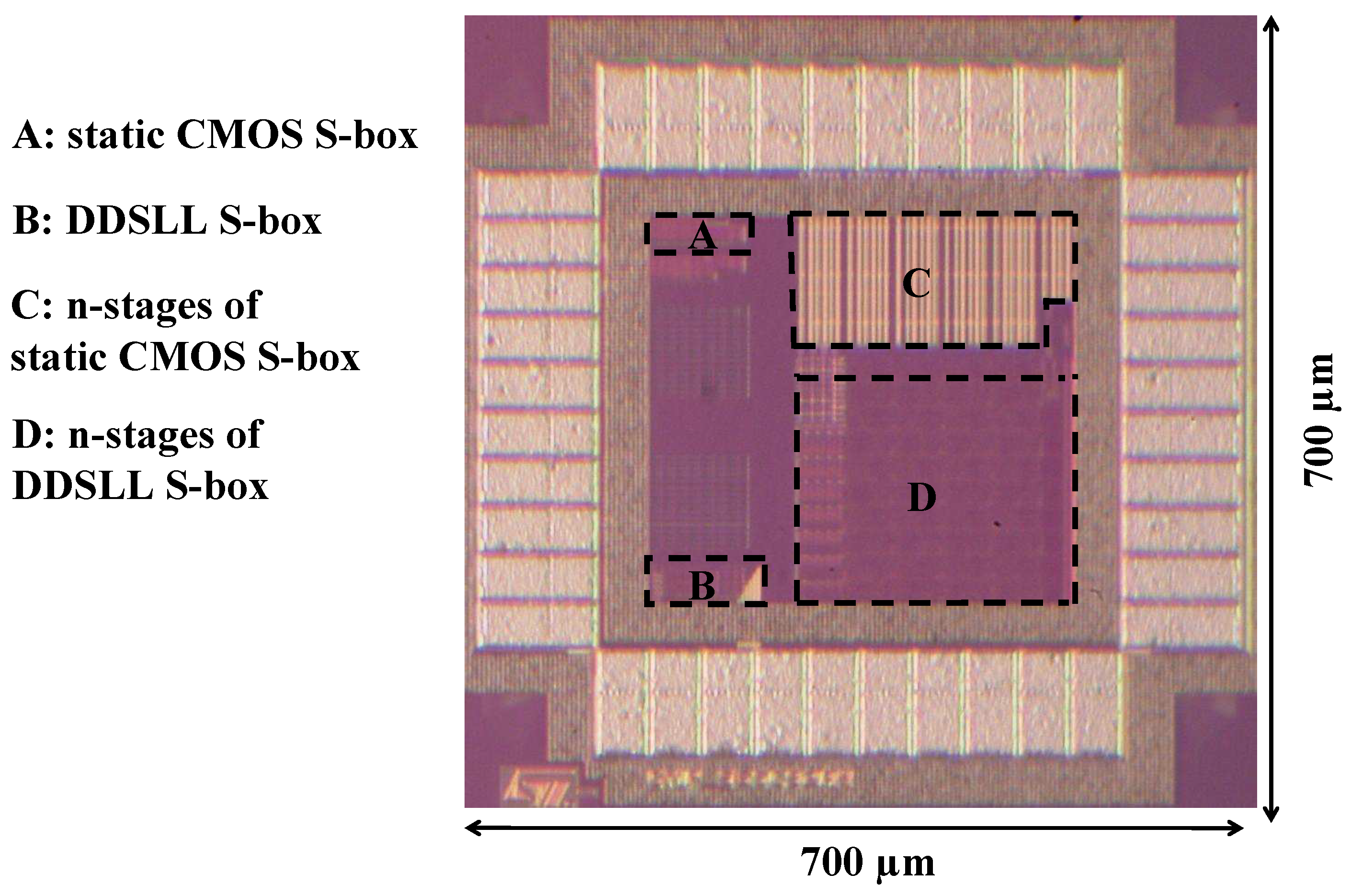
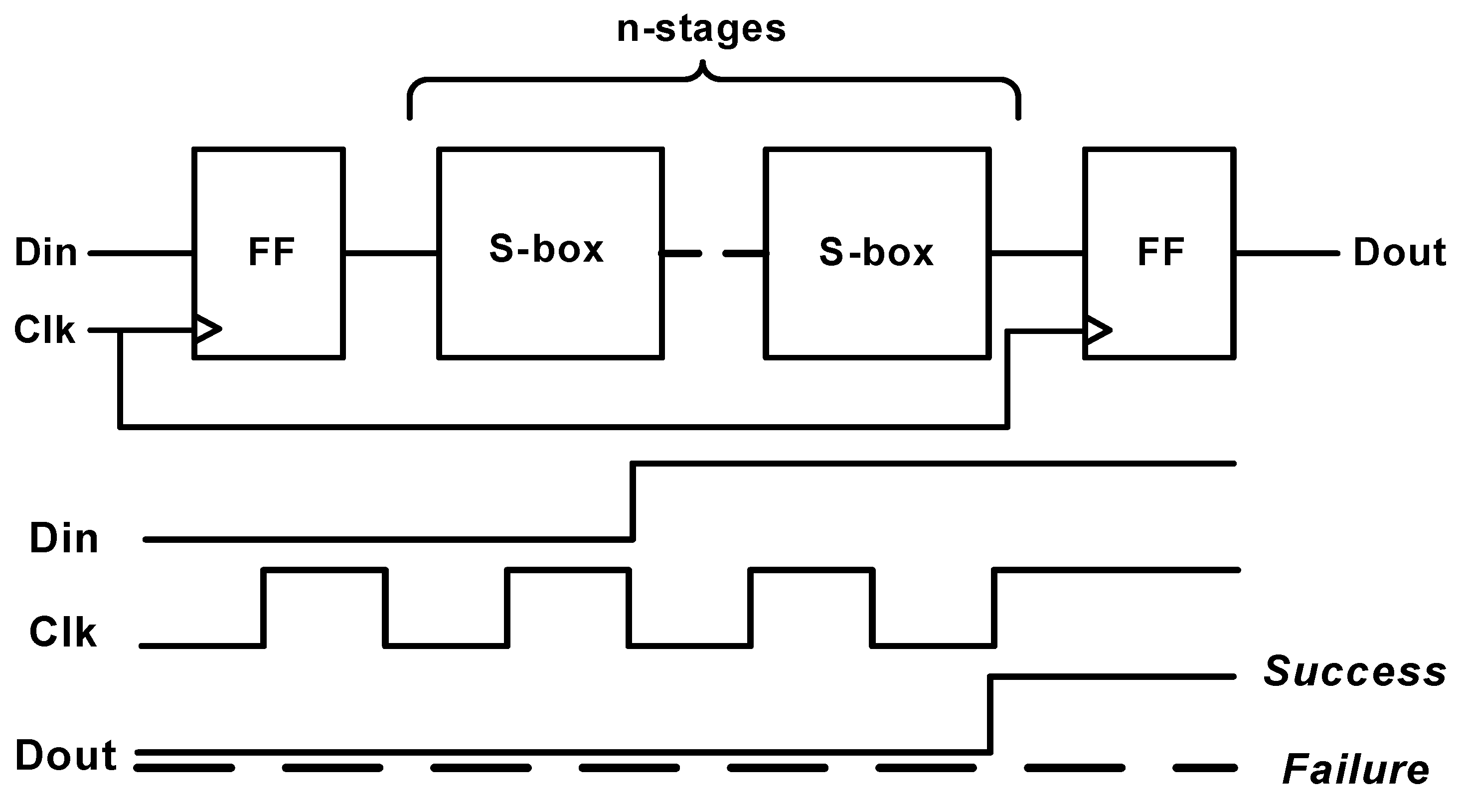
Section 2 describes the DDSLL topology, functionality and circuit design we developed. Simulation results of power, delay, security and dynamic power variability of DDSLL compared to static CMOS are presented in
Section 3. The test chip followed by the measurement results of both DDSLL and static CMOS AES S-boxes are described in
Section 4.
2. Dynamic Differential Swing Limited Logic (DDSLL)
The DDSLL style is one of several DDL self-timed styles developed by [
19] for secure low-power applications. It features a precharge phase where all differential outputs are charged to
VDD. Similar to the DyCML style, DDSLL operates in a self-timing scheme. It employs a dynamic current source to eliminate the static power consumption associated with regular current-mode logic styles. The cut-off of this current source is performed when a feed-back loop detects the completion of the evaluation. If operated with a self-time scheme, the completion signal denoted by ENO (
i.e., ENd of Operation) is propagated to the next logic stage to start its evaluation phase.
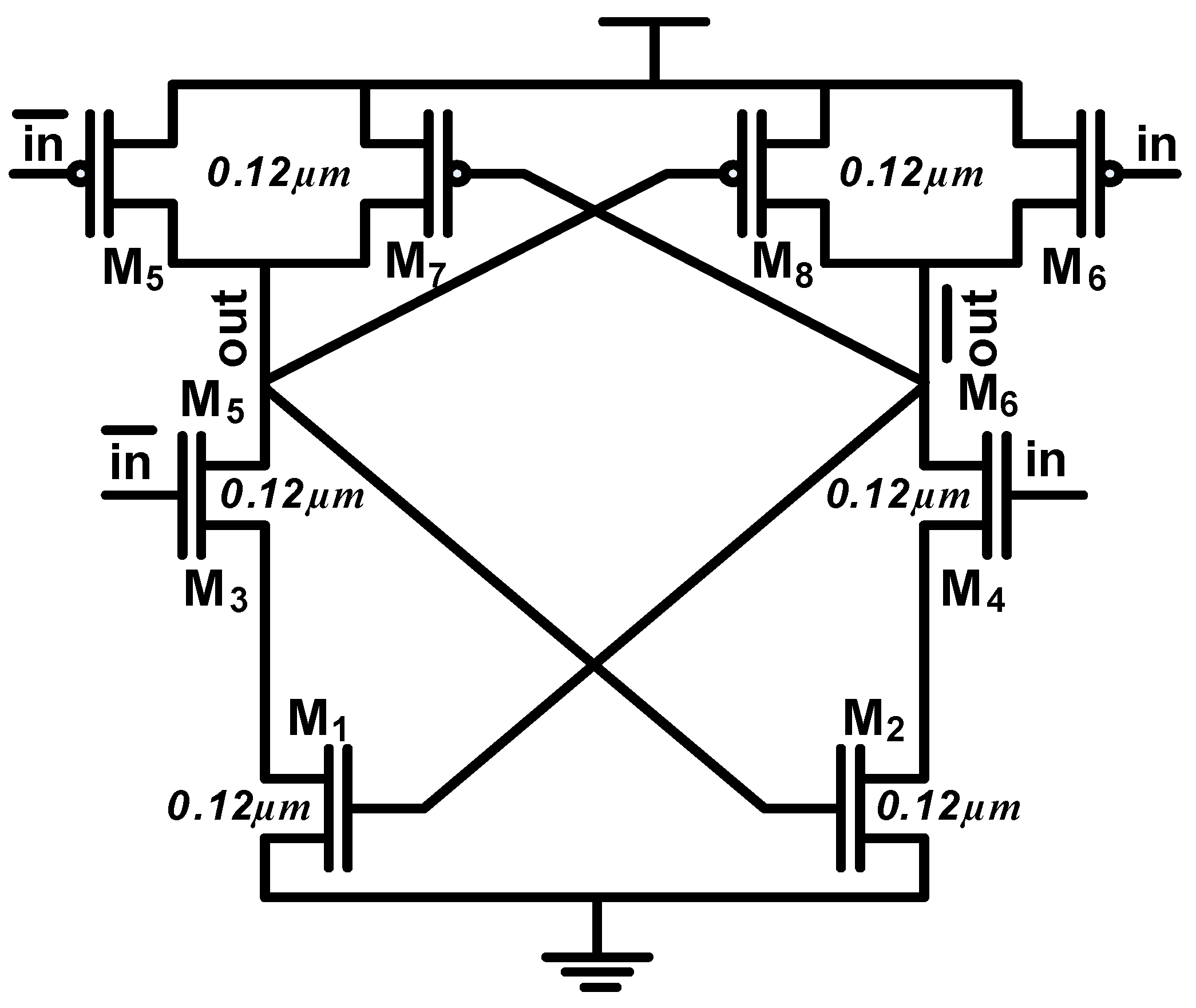
2.1. DDSLL Circuit Topology
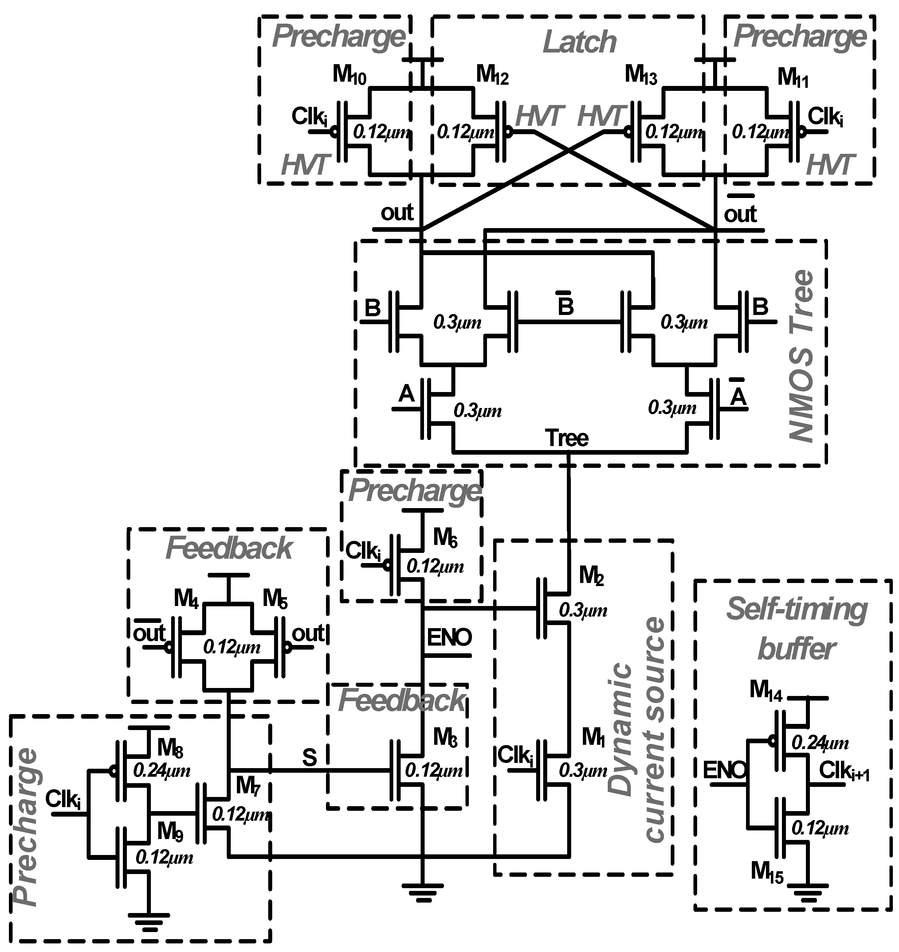
Figure 1 shows the schematics of a simple XOR gate implemented using DDSLL. It uses the same NMOS tree as DyCML to evaluate the function at hand. Transistors
M1 and
M2 operate as the dynamic current source, while transistors
M3–
M5 perform the feed-back operation necessary for cutting off the current after evaluation. Transistors
M6–
M11 form the precharge circuit, and transistors
M12 and
M13 function as a latch. The self-timing buffer used for the DDSLL is a simple inverter as shown in
Figure 1.
2.2. DDSLL Functional Operation
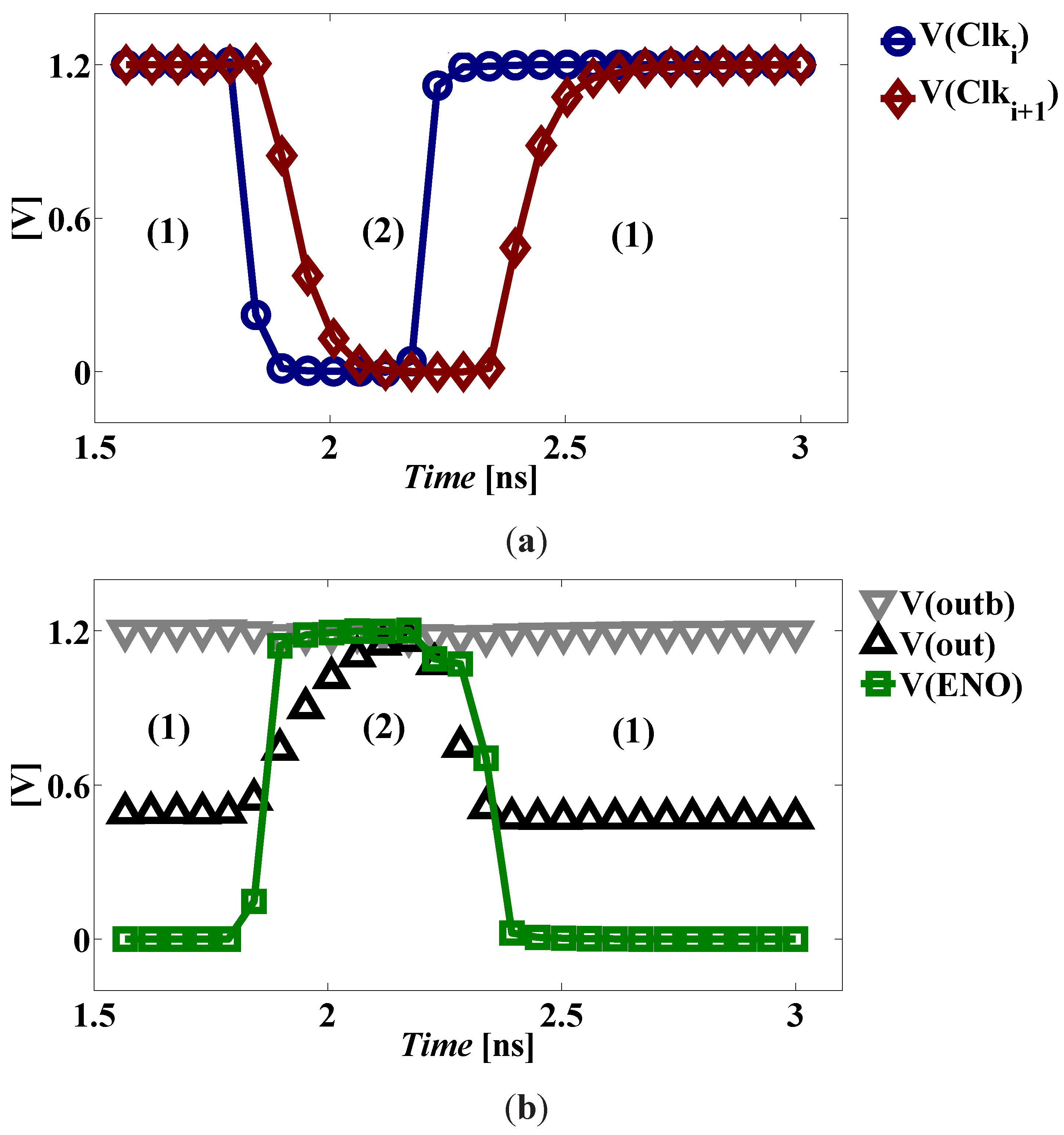
The operation of the DDSLL is quite simple. It consists of two phases: precharge and evaluation.
Figure 2 shows how the precharge and evaluation phases function. During the precharge phase, the input clock signal
Clki is low, discharging node
S to
GN D and charging node
EN O to
VDD. However, there is no current path from
VDD to
GN D as
M1 is switched off. Meanwhile, both output nodes
out and
are precharged to
VDD via transistors
M10 and
M11.
During the evaluation phase, the input clock signal Clki is high, allowing current to flow through the dynamic current source (M1, M2), as node EN O was previously charged to VDD, in order to provide a discharge path for one of the precharged output nodes. Depending on the logic function and the inputs, there will be a single low impedance path from one of the output nodes to GN D. As soon as one of the output nodes falls below VDD − VtP |F B, where VtP |F B is the threshold voltage of the feed-back PMOS transistors, node S will be charged to VDD turning on the feedback transistor M3, which in turn discharges node EN O to GN D switching off the dynamic current source. Meanwhile, one of the latch transistors (M12, M13) turns on as the output node connected to its gate falls below VDD − VtP |L, where VtP |L is the threshold voltage of the latch PMOS transistors, preserving the voltage of the other output node at VDD. The self-timing buffer acts as the interface between cascaded stages of the DDSLL style, as it delivers a slightly shifted version of the input clock indicating the termination of the evaluation phase of the current block.
2.3. DDSLL Circuit Design
As was previously shown in [
33], the choice of the technology node with the appropriate class (either general purpose (GP) or low-power (LP)) and device type greatly affects the circuit delay and power consumption performance. As a result, the LP 65 nm technology node is selected not only because of its economical impact, but also to reduce both the dynamic power and leakage power without sacrificing the performance.
With respect to the sizing of the transistors, all are designed with minimum gate length (Lg = 0.06 µm). As for the transistors width:
The precharge, latch, feed-back circuits and the self-timing buffer are designed using minimum feature size transistors (W = 0.12 µm) to reduce the power consumption except for the PMOS transistors in the inverters of the precharge circuit and self-timing buffer (W = 0.24 µm) to maintain the duty cycle of the input clock.
The dynamic current source uses wider transistors (W = 0.3 µm) in order to drive sufficient current from the NMOS tree during the evaluation period providing the desired output voltage swing.
The NMOS tree is also designed with wider transistors (W = 0.3 µm) for two reasons; the first is to increase the output voltage swing and the second to reduce the effect of WID variability on the output voltage swing.
Regarding the choice of the devices, this technology offers three different threshold-voltages (Vt) devices, low-Vt (LVT), standard-Vt (SVT) and high-Vt (HVT). Most DDSLL devices are chosen to be SVT devices to limit the leakage power without great loss of performance. Contrarily, the latch and transistors M10–M11 of the precharge circuit use HVT devices in order to reduce the leakage that charges the low-voltage output nodes during the evaluation phase especially at higher temperatures.
2.4. NMOS Trees Creation
Since the DDSLL style is developed as a countermeasure against power analysis attacks [
19,
34], special care has to be taken while designing the NMOS trees, especially since large NMOS trees can be used to implement complex functions with even three or four inputs in order to save area.
The NMOS tree representing a certain function can be easily created from the binary decision diagram (BDD) [
36] used to define this function [
37,
38]. Accordingly, a tool based on BDD is proposed in [
38] to explore different implementations of the targeted NMOS trees in order to predict the most secure structure.
From the layout point of view, [
39,
40] propose a technique that employs standard place and route tools to route the differential signals guaranteeing the matching of the interconnect capacitances within a few percent. However in the test chip of this paper, NMOS trees creation and layout are done in a full-custom manner. Although all three above mentioned items are equally important to guarantee input-independent power consumption, only items (1) and (3) are taken into consideration in this test chip. The main reason behind this design choice is to reduce both the power consumption and the area of the DDSLL gates. That is, if the number of series transistors in each branch of an NMOS tree is equalized, then the number of transistors per gate would increase leading to a higher power consumption and an enlarged area. As a result, we decided to implement the most compact NMOS tree considering items (1) and (3) only as a tradeoff between power consumption/area and security performance in this test chip.
2.5. Sharing Principle
The sharing of common blocks is generally used to reduce the power consumption overhead of these blocks and also to reduce the die size. It is applicable to differential current mode logic styles which are either dynamic such as DyCML or static as in MCML [
41,
42,
43]. For example, in subthreshold MCML [
41] the feedback bias circuit, which defines the gate voltage of the PMOS load devices, can be shared among several logic gates. Also in [
43] the replica bias in the subthreshold source coupled logic (STSCL), which biases both the PMOS load devices and the tail current source, can be shared. However, sharing in these cases causes the design to be vulnerable to WID variability as the feedback bias/replica bias should be well matched to the MCML/SCL gates in order to minimize the deviation of the output voltage swing. As a result, a deviation of 40 mV in STCL for minimum size devices using 0.18
µm technology is reported by [
43].
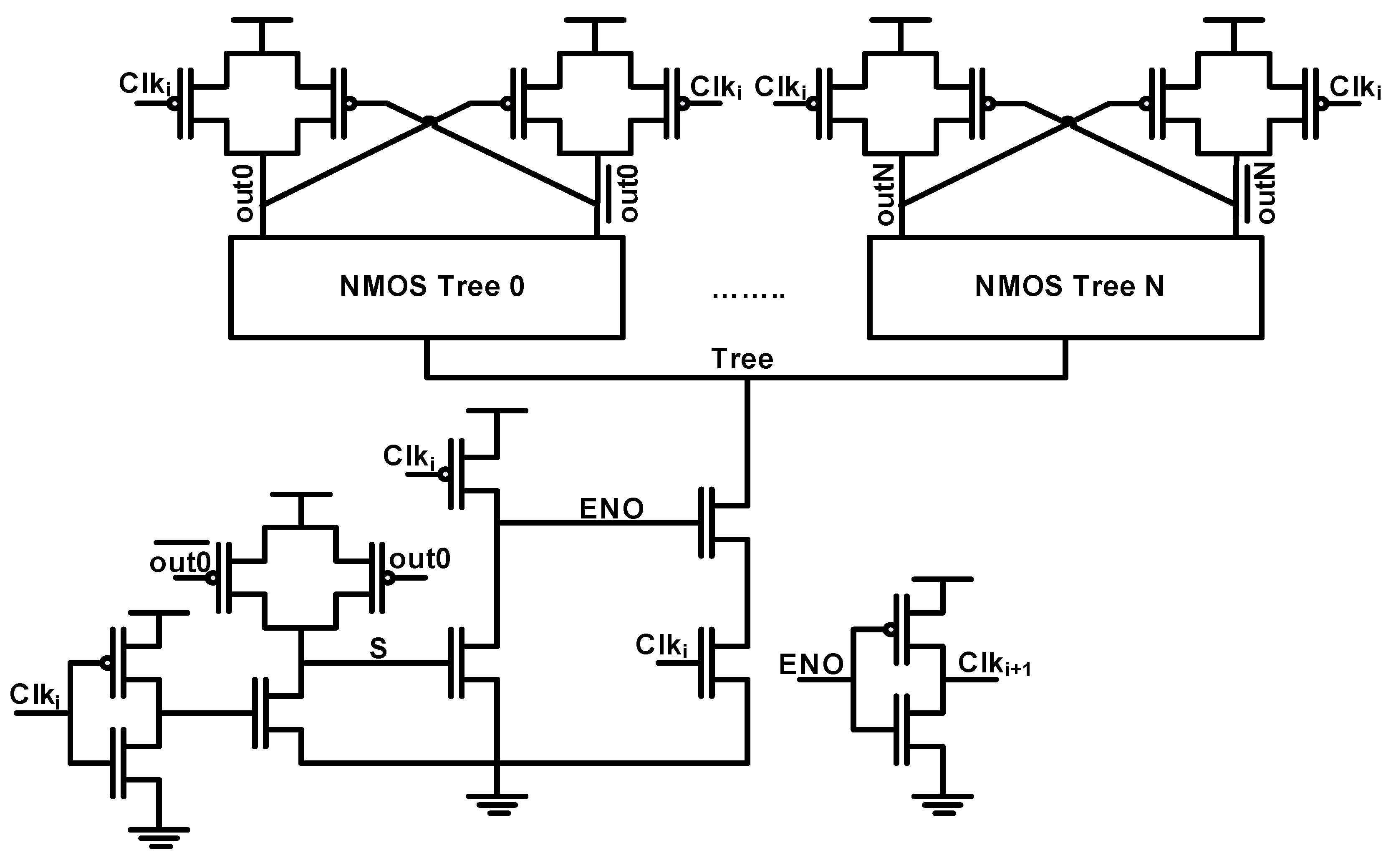
On the other hand, the principle of sharing in DDSLL is quite different.
Figure 3 depicts the technique we introduce so that several NMOS trees can share the same feed-back, dynamic current source, self-timing buffer, and part of the precharge circuit. However, the latch transistors connected to the output nodes cannot be shared as they are needed for each output of the NMOS trees. Also the output precharge transistors are not shared, although they can be, because of the excess complexity that would be added at the layout phase. Accordingly, sharing is useful among gates whose operations can be performed at the same time, since in this case these functions will terminate their evaluation process at the same time. Therefore, they need a single dynamic source and a single self-timing buffer.
Finally, the out/ of the NMOS tree that derive the shared feed-back circuit should be chosen to be the most loaded outputs. This way, the output clock Clki+1 of these shared functions is generated after the slowest output is evaluated which guarantees successful operation. In addition, this will increase the output voltage swing of the shared blocks as the slowest output will cut off the current of the dynamic current source after a longer period.
2.6. Interface with Static CMOS Logic
To interface the output of the DDSLL with the input of the static CMOS, a special buffer is needed to convert the DDSLL low-swing clocked signal to a full-swing non-clocked signal. Low-swing to full-swing buffers exist in literature, for example in [
17]. However, it does not take into account the fact that the differential outputs are both precharged to
VDD every clock cycle, while in static CMOS this is not the case. Therefore, the buffer interface needs not only to convert the low-swing signal to a full-swing signal, but also to preserve the evaluated output during the precharge phase of the clock.
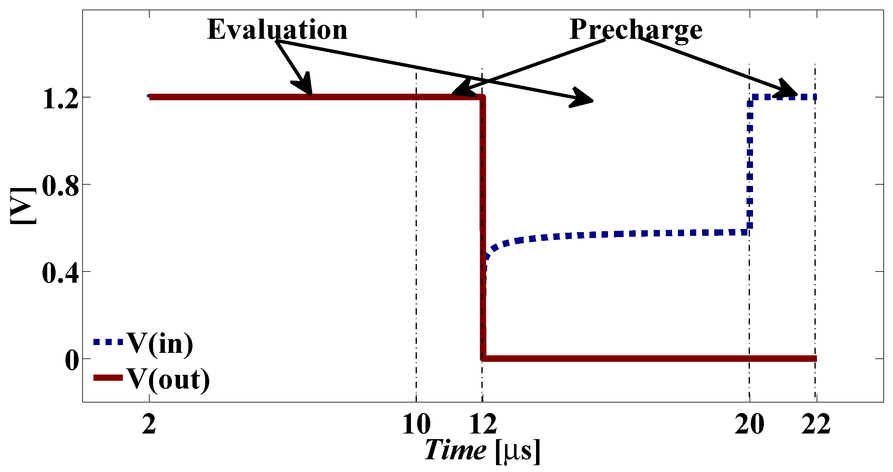
Figure 4 shows the schematic of the proposed output buffer to interface the DDSLL with the static CMOS. All transistors are SVT devices with minimum feature size. The input signals
in and
are the differential low-swing outputs of the DDSLL style, while the
out and
signals are the input signals to the static CMOS. In order to explain the functionality of the output buffer let us assume that during evaluation
in is the low signal and
is the high signal. During the evaluation phase, transistor
M6 is on, charging node
to
VDD, which in turn will switch on transistor
M1. Now the two series NMOS transistors
M1 and
M3 are on discharging node
out to
GN D. During the precharge phase, both
in and
signals are high, turning on transistors
M3 and
M4. As a consequence, the output buffer acts as a latch preserving the voltages of the differential full-swing previously evaluated outputs. The operation of the output buffer is shown in
Figure 5.
On another hand, the interface between the output of the static CMOS and the input of the DDSLL does not require special buffers, it is sufficient to directly connect the output of the static CMOS to the input of the DDSLL similar to [
17].
5. Conclusions
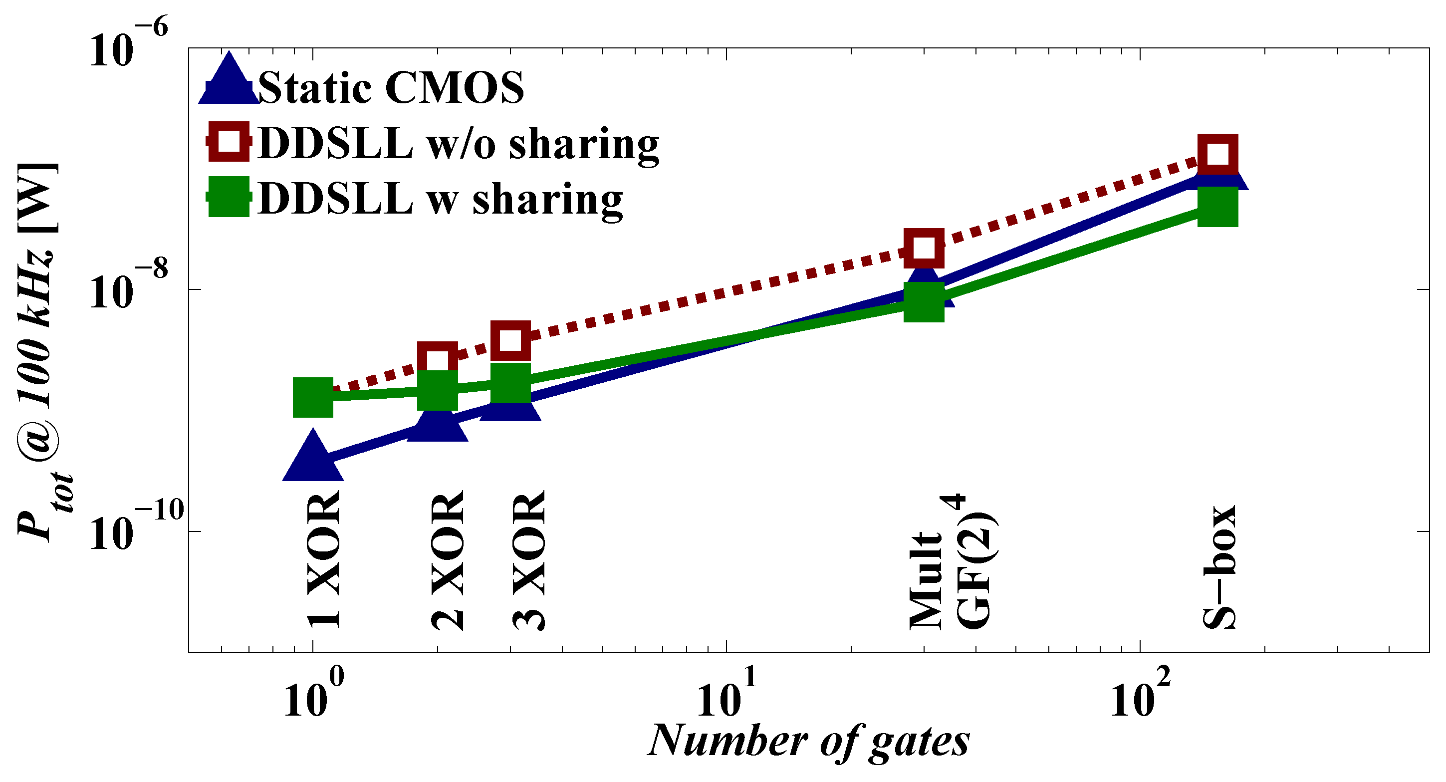
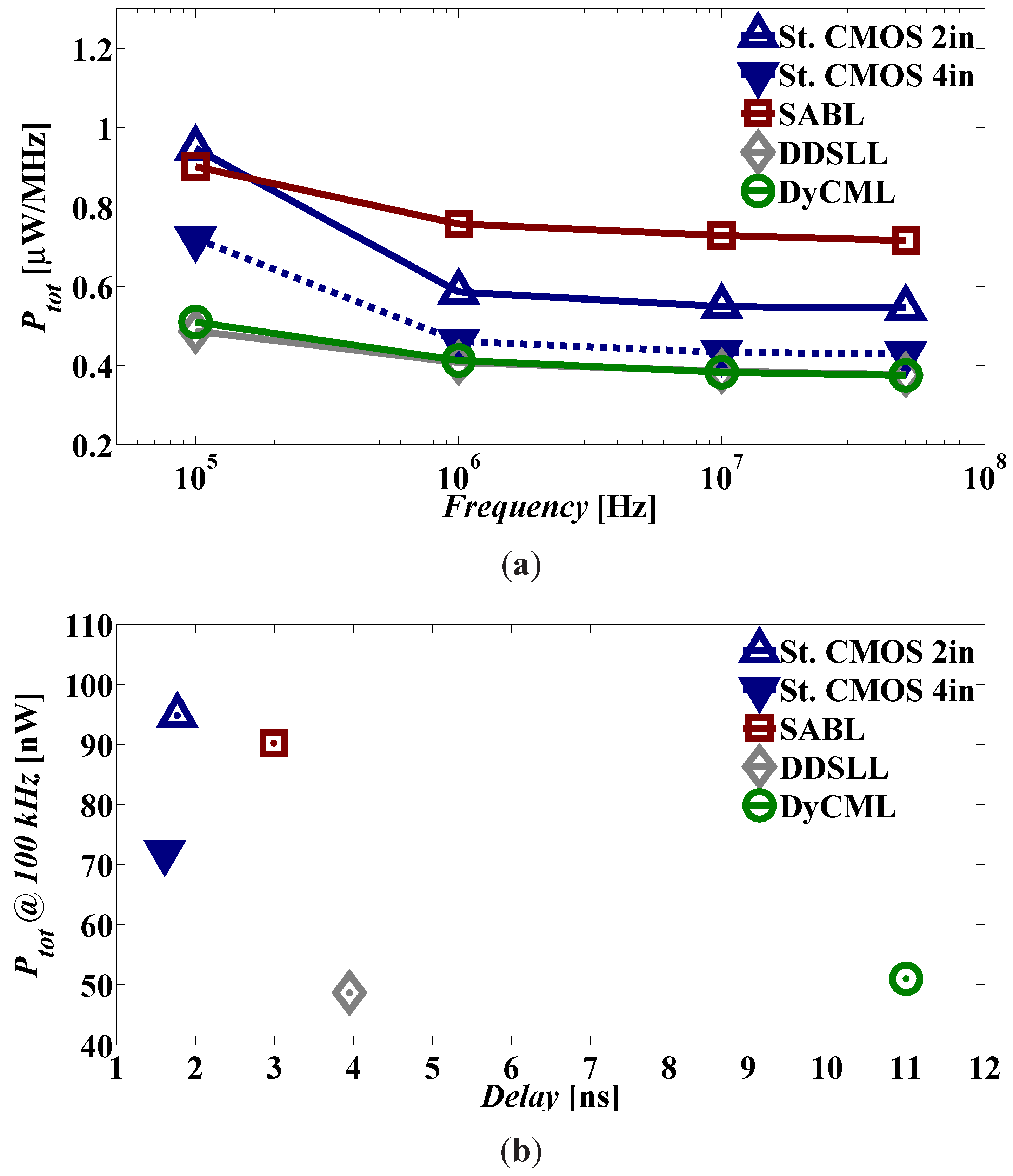
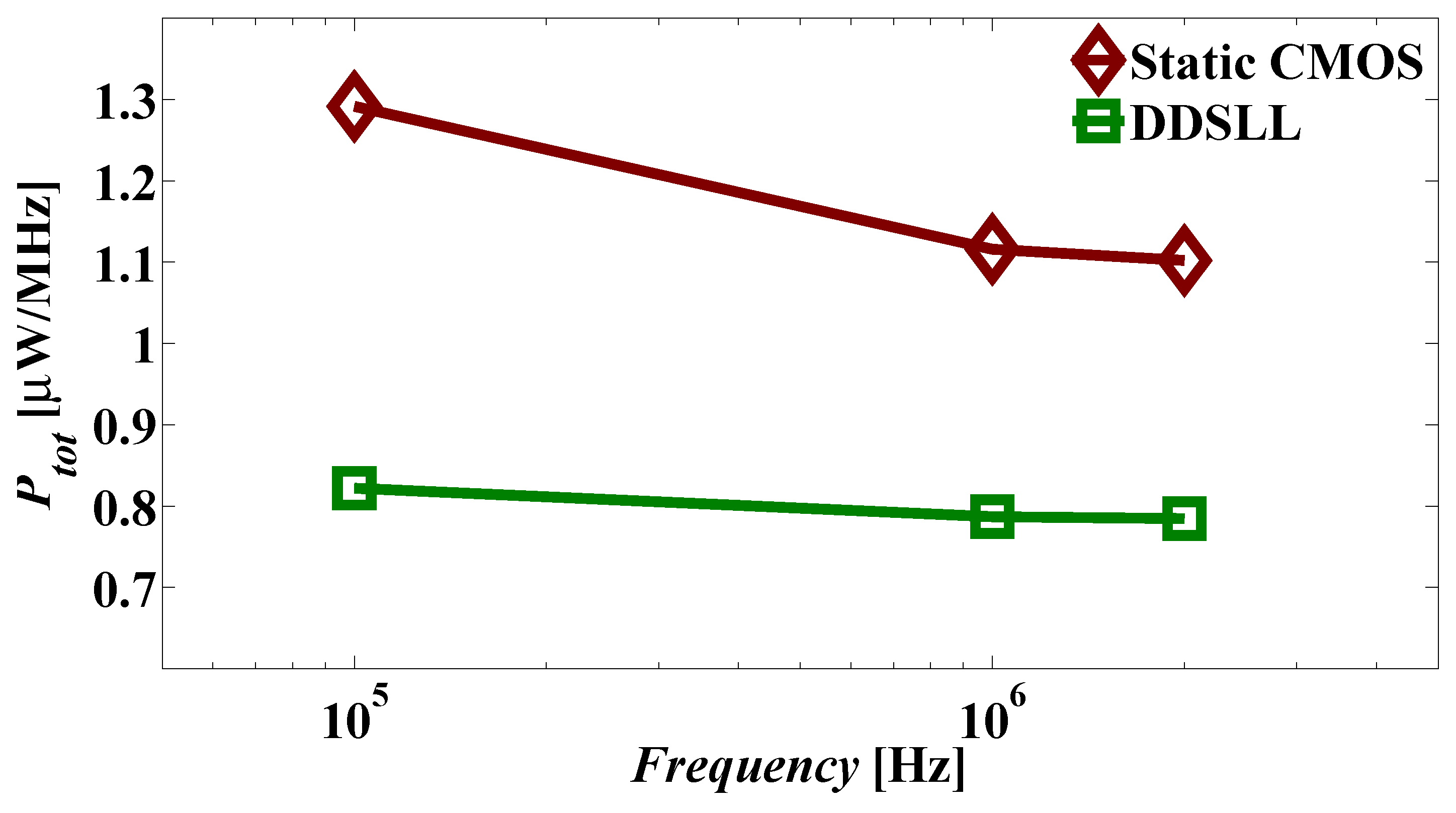
Although static CMOS features low-power operation and small chip area, it fails to comply with the basic requirement of secure applications which is to hide the secure information. Therefore DDL styles were proposed to mitigate this deficiency, among which the DDSLL style. Taking into consideration the two main challenges of low-power secure applications, namely the power consumption and the chip area, DDSLL presents an interesting option as its measured power consumption is 35% less than static CMOS (implemented using 2-input gates). On the other hand, simulation results show that SABL consumes the same power compared to 2-input static CMOS and 31% more power compared to 4-input static CMOS at 100 kHz. It is clearly seen that DDSLL is more power efficient than SABL. Furthermore, the chip area of the DDSLL S-box is only 12% larger than static CMOS. However, the main drawback of DDSLL is the delay penalty which is 2.5×, but for relaxed timing constraint applications such as RFIDs and smart cards this is not an issue. In this work we also emphasize the importance of sharing the common blocks as it reduces the power consumption of the S-box 63%.
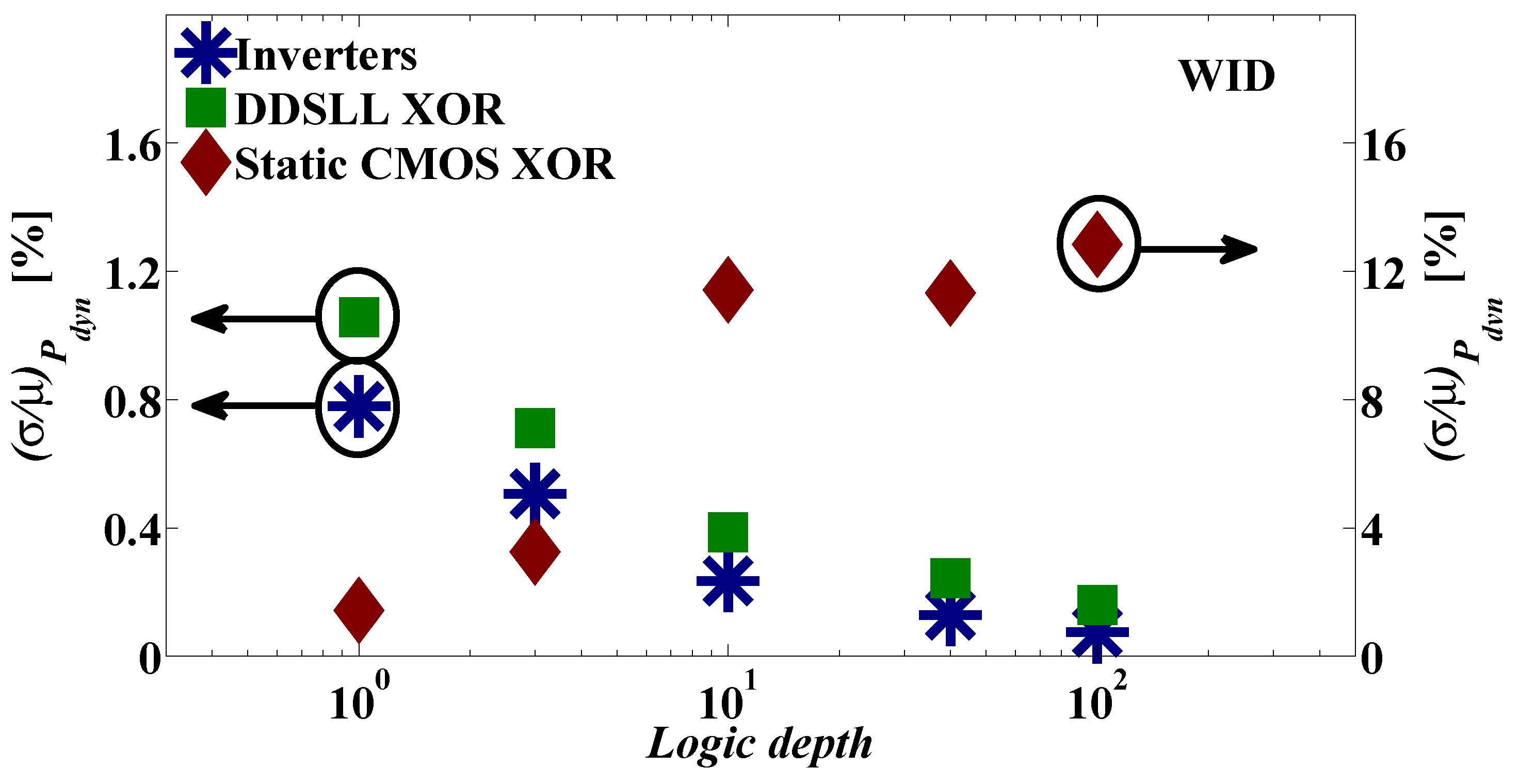
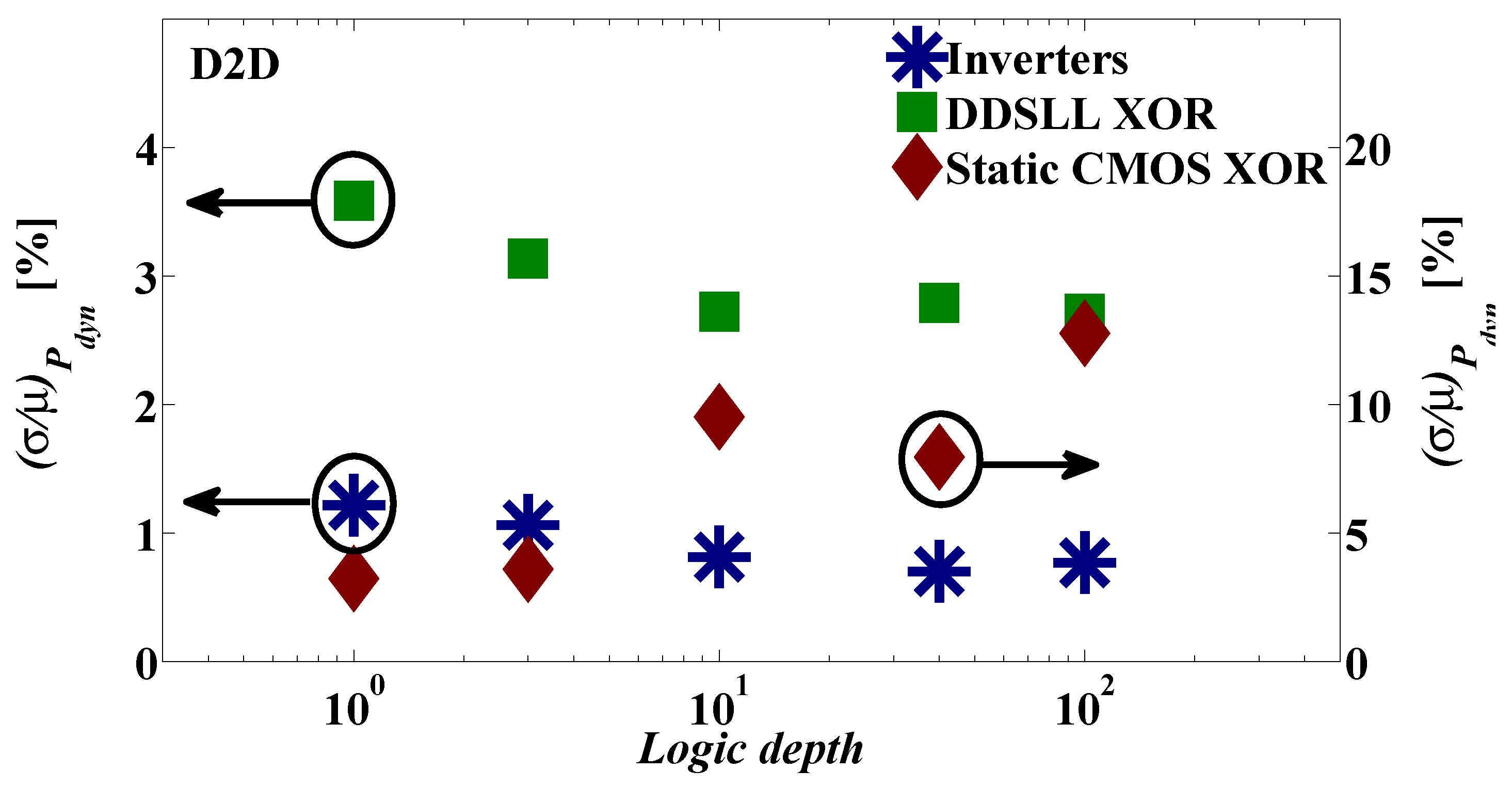
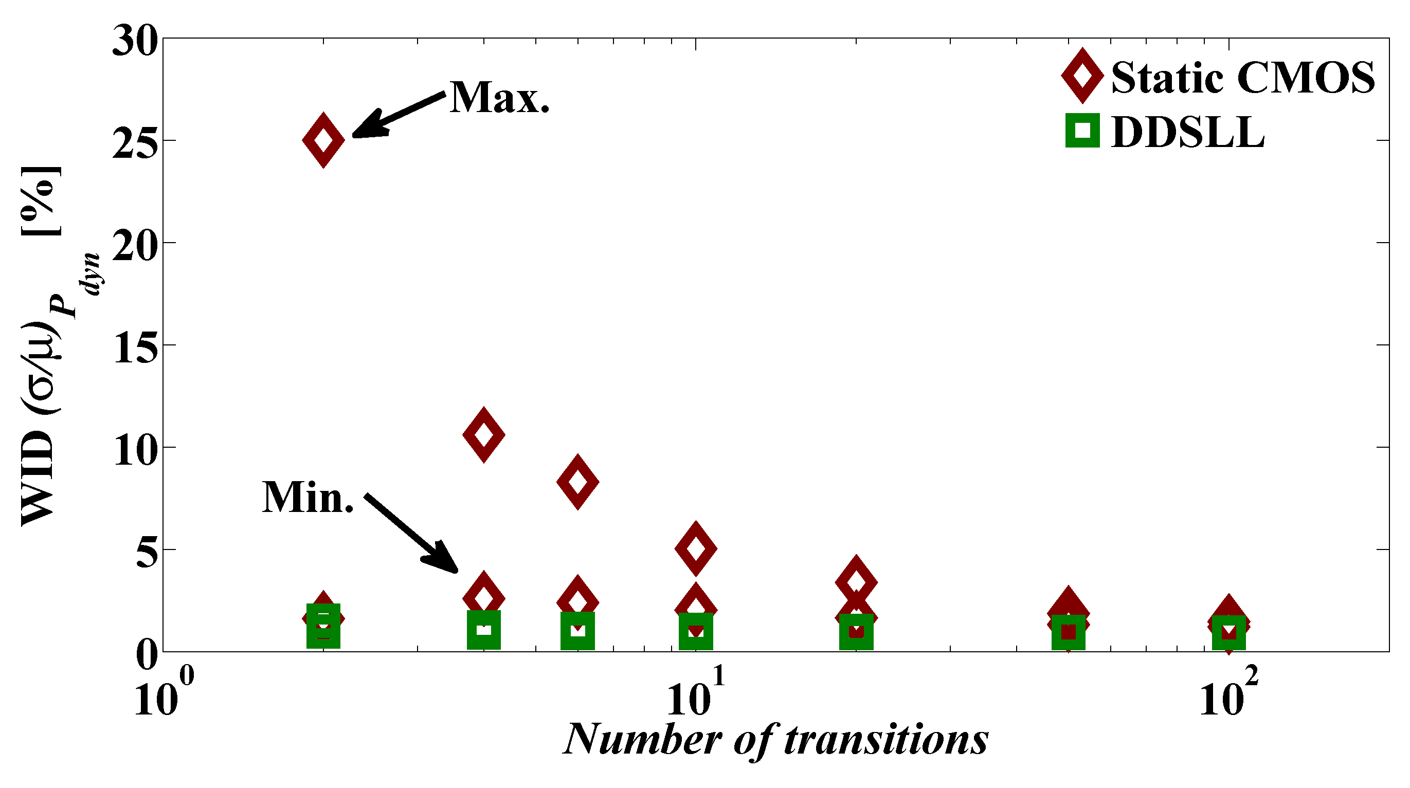
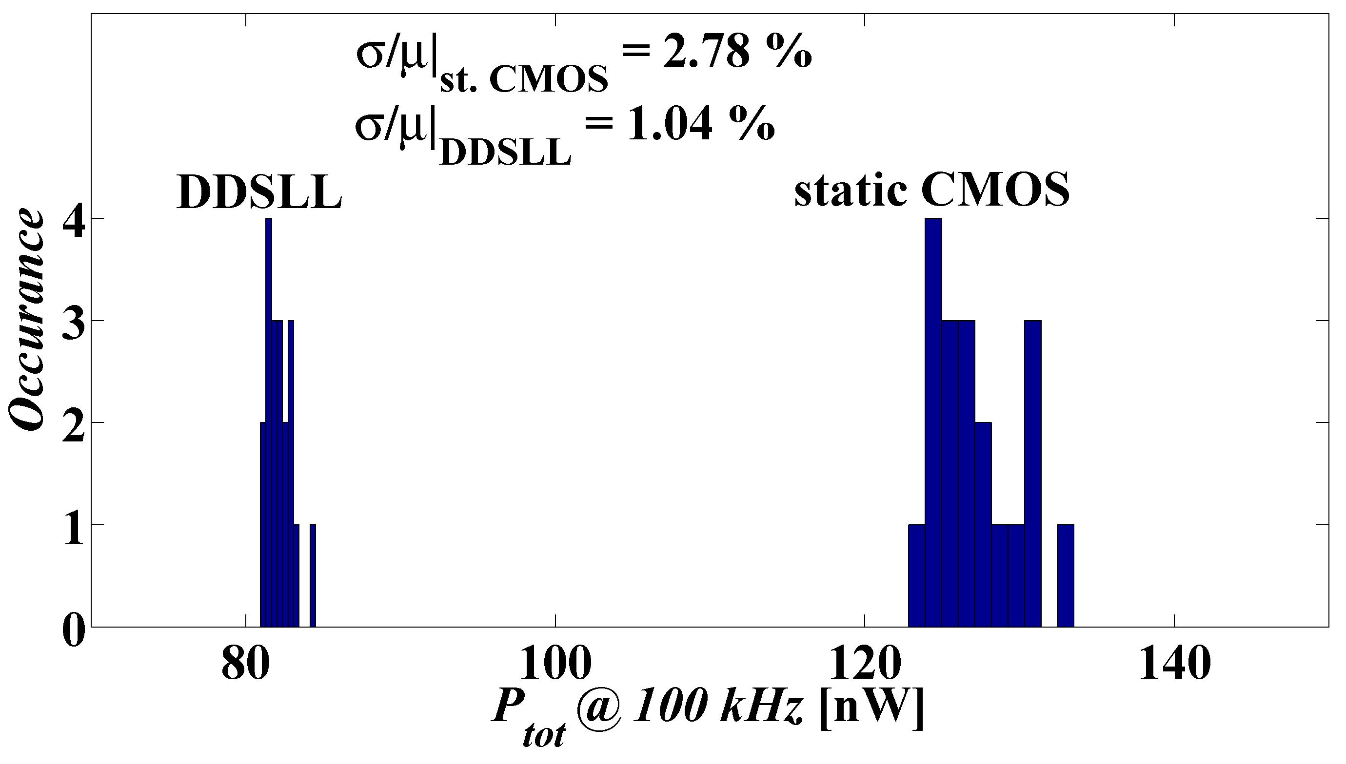
Although process variability is considered to improve the security performance of static CMOS against PA attacks, it is studied here from another perspective. The variability of the dynamic power consumption of the DDSLL style (which is also applicable to similar DDL styles) is addressed for the first time to the authors’ knowledge. The dynamic power consumption of DDSLL features constant WID and D2D variabilities thanks to its glitch-free operation, whereas static CMOS shows a great dependency on the activity factor as the logic depth increases. As a result, the worst case dynamic power ratio between static CMOS S-box and DDSLL S-box would be 2.65× as demonstrated by Monte-Carlo simulation results (considering here the total power of DDSLL instead of its dynamic power since its static power is proved to be negligible).
As for the security assessment, using the perceived information metric, measured results of DDSLL demonstrate a 3× security improvement over its static CMOS counterpart. Nevertheless from simulations, the DyCML style proves to be the most secure logic as it has a security margin of 2.7× with respect to static CMOS, compared to 2× and 1.5× for DDSLL and SABL styles, respectively. Yet, DDSLL provides a better low-power area-efficient solution compared to other DDL styles with significantly enhanced security performance compared to static CMOS.


