Abstract
This paper develops an ultra-low power asynchronous circuit design methodology, called Multi-Threshold NULL Convention Logic (MTNCL), also known as Sleep Convention Logic (SCL), which combines Multi-Threshold CMOS (MTCMOS) with NULL Convention Logic (NCL), to yield significant power reduction without any of the drawbacks of applying MTCMOS to synchronous circuits. In contrast to other power reduction techniques that usually result in large area overhead, MTNCL circuits are actually smaller than their original NCL versions. MTNCL utilizes high-Vt transistors to gate power and ground of a low-Vt logic block to provide for both fast switching and very low leakage power when idle. To demonstrate the advantages of MTNCL, a number of 32-bit IEEE single-precision floating-point co-processors were designed for comparison using the 1.2 V IBM 8RF-LM 130 nm CMOS process: original NCL, MTNCL with just combinational logic (C/L) slept, Bit-Wise MTNCL (BWMTNCL), MTNCL with C/L and completion logic slept, MTNCL with C/L, completion logic, and registers slept, MTNCL with Safe Sleep architecture, and synchronous MTCMOS. These designs are compared in terms of throughput, area, dynamic energy, and idle power, showing the tradeoffs between the various MTNCL architectures, and that the best MTNCL design is much better than the original NCL design in all aspects, and much better than the synchronous MTCMOS design in terms of area, energy per operation, and idle power, although the synchronous design can operate faster.
1. Introduction
With the current trend of semiconductor devices scaling into the deep submicron region, design challenges that were previously minor issues have now become increasingly important. Where in the past, dynamic switching power has been the predominant factor in CMOS digital circuit power dissipation, recently, with the dramatic decrease of supply and threshold voltages, a significant growth in leakage power demands new design methodologies for digital Integrated Circuits (ICs). The main component of leakage power is sub-threshold leakage, caused by current flow through a transistor even if it is supposedly turned off. Sub-threshold leakage increases exponentially with decreasing transistor feature size.
Among the many techniques proposed to control or minimize leakage power in deep submicron technology, Multi-Threshold CMOS (MTCMOS) [1], which reduces leakage power by disconnecting the power supply from the circuit during idle (or sleep) mode while maintaining high performance in active mode, is very promising. MTCMOS incorporates transistors with two or more different threshold voltages (Vt) in a circuit. Low-Vt transistors offer fast speed but have high leakage, whereas high-Vt transistors have reduced speed but far less leakage current. MTCMOS combines these two types of transistors by utilizing low-Vt transistors for circuit switching to preserve performance, and high-Vt transistors to gate the circuit power supply to significantly decrease sub-threshold leakage.
Quasi-delay-insensitive (QDI) NULL Convention Logic (NCL) circuits [2], designed using CMOS, exhibit an inherent idle behavior since they only switch when useful work is being performed; however, there is still significant leakage power during idle mode. This paper combines the MTCMOS technique with NCL to sleep the NCL circuit during idle mode, in lieu of the NULL cycle, to yield a fast ultra-low power asynchronous circuit design methodology, called Multi-Threshold NULL Convention Logic (MTNCL), also referred to as Sleep Convention Logic (SCL), which requires less area than the original NCL circuit.
Section 2 provides an overview of NCL, MTCMOS, and previous MTNCL implementations. Section 3 develops enhancements to the MTNCL technique that allows for both registration and completion logic to be slept along with the combinational logic (C/L). Section 4 compares the various implementations; and Section 5 provides conclusions.
2. Previous Work
2.1. Introduction to NCL
NCL circuits utilize multi-rail logic, such as dual-rail, to achieve delay-insensitivity. A dual-rail signal, D, consists of two wires, D0 and D1, which may assume any value from the set {DATA0, DATA1, NULL}. The DATA0 state (D0 = 1, D1 = 0) corresponds to a Boolean logic 0, the DATA1 state (D0 = 0, D1 = 1) corresponds to a Boolean logic 1, and the NULL state (D0 = 0, D1 = 0) corresponds to the empty set, meaning that the value of D is not yet available. The two rails are mutually exclusive, such that both rails can never be asserted simultaneously; this state is defined as an illegal state. Dual-rail logic is a space optimal 1-hot delay-insensitive code, requiring two wires per bit.
NCL circuits are comprised of 27 fundamental gates [3]. These 27 gates constitute the set of all functions consisting of four or fewer variables. Here, a variable refers to one rail of a multi-rail signal; hence, a four variable function is not the same as a function of four literals, which would consist of eight variables, assuming dual-rail logic. The primary type of threshold gate, shown in Figure 1, is the THmn gate, where 1 ≤ m ≤ n. THmn gates have n inputs; at least m of the n inputs must be asserted before the output will become asserted; and NCL threshold gates are designed with hysteresis state-holding capability, such that all asserted inputs must be de-asserted before the output will be de-asserted. Hysteresis ensures a complete transition of inputs back to NULL before asserting the output associated with the next wavefront of input data. Therefore, a THnn gate is equivalent to an n-input C-element [4] and a TH1n gate is equivalent to an n-input OR gate. Besides the static NCL gate implementation, shown in Figure 2, there are other CMOS implementations, as detailed in [5,6]. In a THmn gate, each of the n inputs is connected to the rounded portion of the gate; the output emanates from the pointed end of the gate; and the gate’s threshold value, m, is written inside of the gate. NCL threshold gates may also include a reset input to initialize the output. These resettable gates are used in the design of DI registers [7].
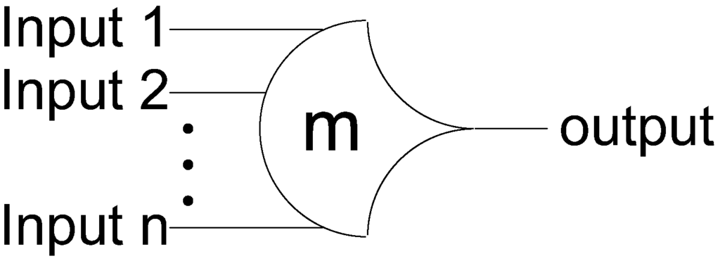
Figure 1.
THmn threshold gate.
Figure 1.
THmn threshold gate.

NCL systems contain at least two DI registers, one at both the input and at the output, and can be finely pipelined by inserting additional registers, as shown in Figure 3. Two adjacent register stages interact through their request and acknowledge signals, Ki and Ko, respectively, to prevent the current DATA wavefront from overwriting the previous DATA wavefront, by ensuring that the two DATA wavefronts are always separated by a NULL wavefront. The acknowledge signals are combined in the Completion Detection circuitry to produce the request signal(s) to the previous register stage, utilizing either the full-word or bit-wise completion strategy [7].
To ensure delay-insensitivity, NCL circuits must adhere to the following criteria: Input-Completeness and Observability [8]. Input-Completeness requires that all outputs of a combinational circuit may not transition from NULL to DATA until all inputs have transitioned from NULL to DATA, and that all outputs of a combinational circuit may not transition from DATA to NULL until all inputs have transitioned from DATA to NULL. In circuits with multiple outputs, it is acceptable according to Seitz’s “weak conditions” of DI signaling [9] for some of the outputs to transition without having a complete input set present, as long as all outputs cannot transition before all inputs arrive. Observability requires that no orphans may propagate through a gate [10]. An orphan is defined as a wire that transitions during the current DATA wavefront, but is not used in the determination of the output. Orphans are caused by wire forks and can be neglected through the isochronic fork assumption [11,12], as long as they are not allowed to cross a gate boundary. This observability condition, also referred to as indicatability or stability, ensures that every gate transition is observable at the output, which means that every gate that transitions is necessary to transition at least one of the outputs.
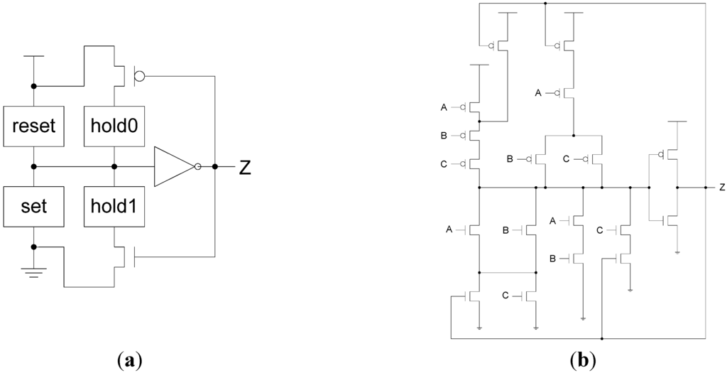
Figure 2.
NCL threshold gate design. (a) General static implementation; (b) TH23 static implementation.
Figure 2.
NCL threshold gate design. (a) General static implementation; (b) TH23 static implementation.

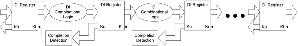
Figure 3.
NCL system framework: input wavefronts are controlled by local handshaking and Completion Detection signals.
Figure 3.
NCL system framework: input wavefronts are controlled by local handshaking and Completion Detection signals.
2.2. Introduction to MTCMOS
MTCMOS reduces leakage power by disconnecting the power supply from the circuit during idle (or sleep) mode while maintaining high performance in active mode, by utilizing different transistor threshold voltages (Vt) [1]. Low-Vt transistors are faster but have high leakage, whereas high-Vt transistors are slower but have far less leakage current. MTCMOS combines these two types of transistors by utilizing low-Vt transistors for circuit switching to preserve performance and high-Vt transistors to gate the circuit power supply to significantly decrease sub-threshold leakage.
One MTCMOS method uses low-Vt transistors for critical paths to maintain high performance, while using slower high-Vt transistors for the non-critical paths to reduce leakage. Besides this path replacement methodology, there are two other architectures for implementing MTCMOS. A course-grained technique investigated in [13] uses low-Vt logic for all circuit functions, and gates the power to entire logic blocks with high-Vt sleep transistors, denoted by a dotted circle, as shown in Figure 4. The sleep transistors are controlled by a Sleep signal. During active mode, the Sleep signal is de-asserted, causing both high-Vt transistors to turn on and provide a virtual power and ground to the low-Vt logic. When the circuit is idle, the Sleep signal is asserted, forcing both high-Vt transistors to turn off and disconnect power from the low-Vt logic, resulting in a very low sub-threshold leakage current. One major drawback of this method is that partitioning the circuit into appropriate logic blocks and sleep transistor sizing is difficult for large circuits. An alternative fine-grained architecture, shown in Figure 5, incorporates the MTCMOS technique within every gate [14], using low-Vt transistors for the Pull-Up Network (PUN) and Pull-Down Network (PDN) and a high-Vt transistor to gate the leakage current between the two networks. Two additional low-Vt transistors are included in parallel with the PUN and PDN to maintain nearly equivalent voltage potential across these networks during sleep mode (i.e., X1 is approximately VDD and X2 is approximately GND). Implementing MTCMOS within each gate solves the problems of logic block partitioning and sleep transistor sizing, since each gate is sized separately comprising the gate library; however, this results in a large area overhead.

Figure 4.
General MTCMOS circuit architecture [13].
Figure 4.
General MTCMOS circuit architecture [13].
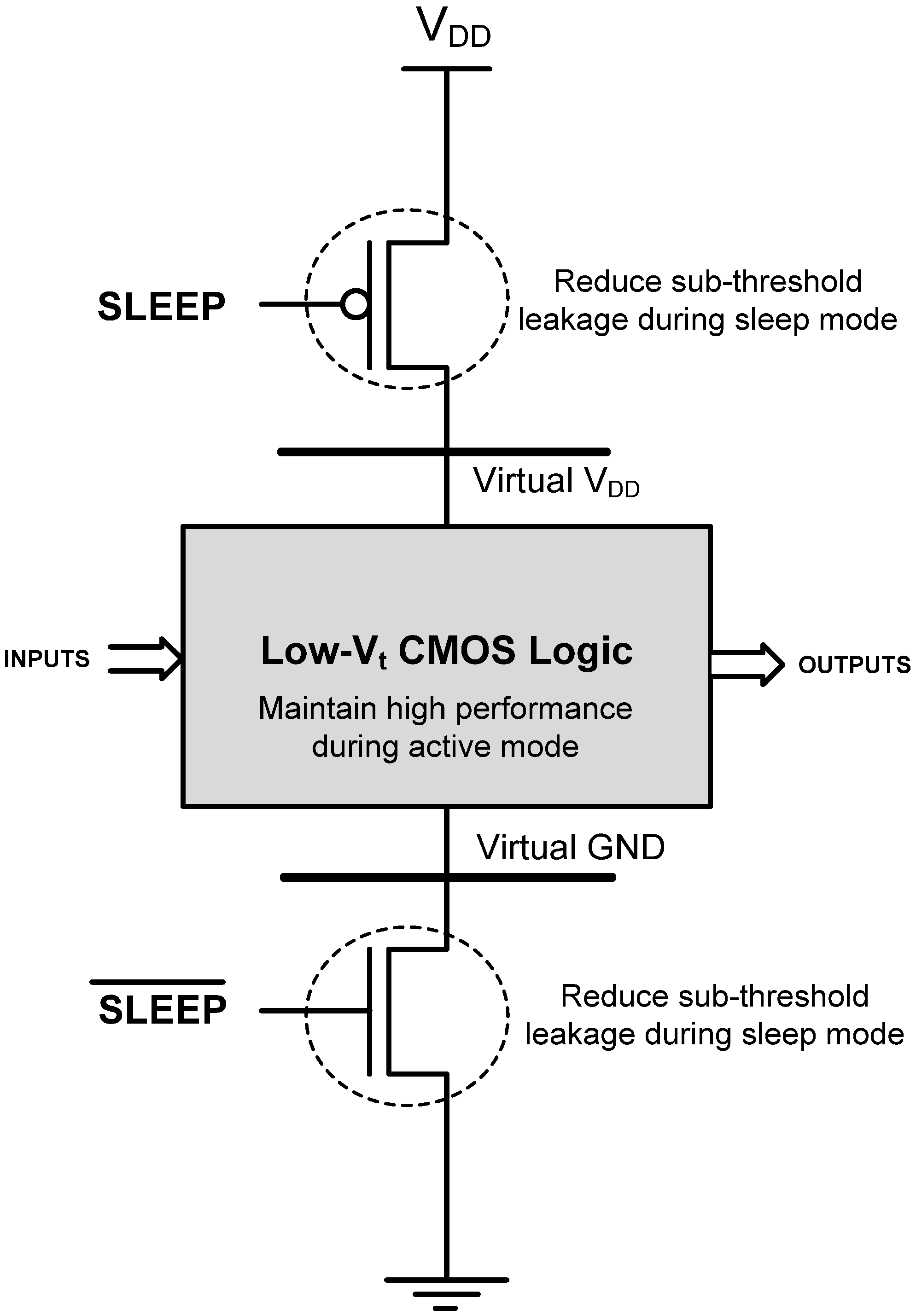
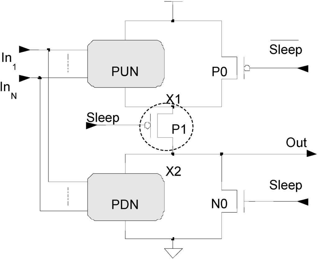
Figure 5.
MTCMOS applied to a Boolean gate [14].
Figure 5.
MTCMOS applied to a Boolean gate [14].

In general, three serious drawbacks hinder the widespread usage of MTCMOS in synchronous circuits [13]: (1) the generation of Sleep signals is timing critical, often requiring complex logic circuits; (2) synchronous storage elements lose data when the power transistors are turned off during sleep mode, although this can be solved with special register designs; and (3) logic block partitioning and transistor sizing is very difficult for the course-grained approach, which is critical for correct circuit operation, and the fine-grained approach requires a large area overhead. However, all three of these drawbacks are eliminated by utilizing NCL in conjunction with the MTCMOS technique.
2.3. Introduction to MTNCL
MTNCL was originally developed in [15,16,17,18,19], as summarized below, while this paper provides significant enhancements to the original MTNCL concept.
2.3.1. Early-Completion Input-Incomplete (ECII) MTNCL Architecture
NCL threshold gates are larger and implement more complicated functions than basic Boolean gates, such that fewer threshold gates are normally needed to implement an arbitrary function compared to the number of Boolean gates; however, the NCL implementation often requires more transistors. Therefore, incorporating MTCMOS inside each threshold gate facilitates easy sleep transistor sizing without requiring as large of an area overhead. Since floating nodes may result in substantial short circuit power consumption at the following stage, an MTCMOS structure similar to the one shown in Figure 5 is used to pull the output node to ground during sleep mode. When all MTNCL gates in a pipeline stage are in sleep mode, such that all gate outputs are logic 0, this condition is equivalent to the pipeline stage being in the NULL state. Hence, after each DATA cycle, all MTNCL gates in a pipeline stage can be forced to output logic 0 by asserting the sleep control signal instead of propagating a NULL wavefront through the stage, such that data is not lost during sleep mode.
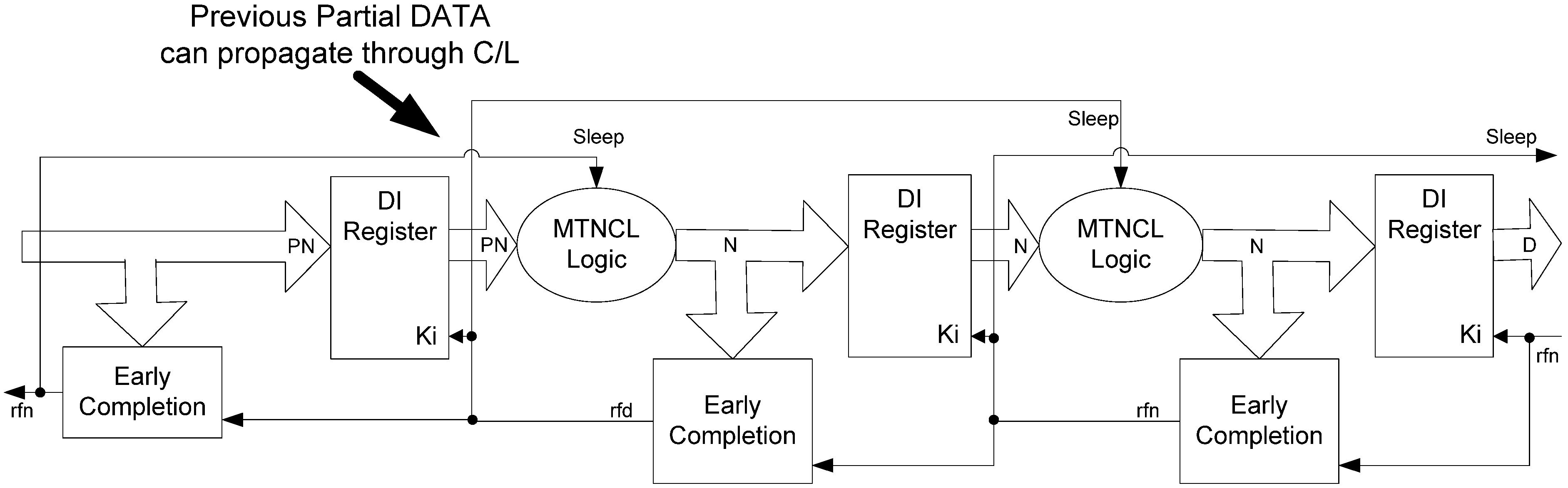
Since the completion detection signal, Ko, indicates whether the corresponding pipeline stage is ready to undergo a DATA or NULL cycle, Ko can be naturally used as the sleep control signal, without requiring any additional hardware, in contrast to the complex Sleep signal generation circuitry needed for synchronous MTCMOS circuits. Unfortunately, the direct implementation of this idea using regular NCL completion compromises delay-insensitivity [18]. To solve this problem, Early Completion [20] can be used in lieu of regular completion, as shown in Figure 6, where each completion signal is used as the sleep signal for all threshold gates in the subsequent pipeline stage. Early Completion utilizes the inputs of registeri-1 along with the Ki request to registeri−1, instead of just the outputs of registeri-1 as in regular completion, to generate the request signal to registeri−2, Koi−1. The combinational logic will not be put to sleep until all inputs are NULL and the stage is requesting NULL; therefore, the NULL wavefront is ready to propagate through the stage, so the stage can instead be put to sleep without compromising delay-insensitivity. The stage will then remain in sleep mode until all inputs are DATA and the stage is requesting DATA, and is therefore ready to evaluate. This Early Completion MTNCL architecture, denoted as ECII, ensures input-completeness through the sleep mechanism (i.e., the circuit is only put to sleep after all inputs are NULL, when all gates are then simultaneously forced to logic 0, and only makes an evaluation after all inputs are DATA), such that input-incomplete logic functions can be used to design the circuit, which decreases area and power and increases speed. Note that sleeping the C/L in lieu of propagating a NULL wavefront compromises observability, such that all C/L gates whose outputs are not inputs to the subsequent register are unobservable. While this makes the architecture less theoretically delay-insensitive, in practice this additional delay sensitivity will not cause problems, as long as the sleep trees are constructed such that there is not a large delay between sleeping the C/L output gates and gates internal to the C/L. This sleep tree timing requirement is easily achievable.
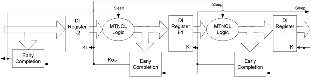
Figure 6.
MTNCL pipeline architecture using Early Completion.
Figure 6.
MTNCL pipeline architecture using Early Completion.

2.3.2. MTNCL Threshold Gate Design for ECII Architecture
The MTCMOS structure is incorporated inside each NCL threshold gate, and actually results in a number of the original transistors no longer being needed. As shown in Figure 7a, the reset circuitry is no longer needed, since the gate output will now be forced to NULL by the MTCMOS sleep mechanism, instead of by all inputs becoming logic 0. hold1 is used to ensure that the gate remains asserted, once it has become asserted, until all inputs are de-asserted, in order to guarantee input-completeness with respect to the NULL wavefront; however, since the ECII architecture guarantees input-completeness through the sleep mechanism, as explained in Section 2.3.1, it follows that NCL gate hysteresis is no longer required. Hence, the hold1 circuitry and corresponding NMOS transistor are removed, and the PMOS transistor is removed to maintain the complementary nature of CMOS logic (i.e., set and hold0 are complements of each other), such that the gate is never floating.
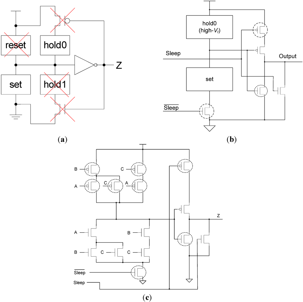
Figure 7.
(a) Incorporating MTCMOS into NCL threshold gates; (b) SMTNCL gate structure; (c) TH23 implementation.
Figure 7.
(a) Incorporating MTCMOS into NCL threshold gates; (b) SMTNCL gate structure; (c) TH23 implementation.
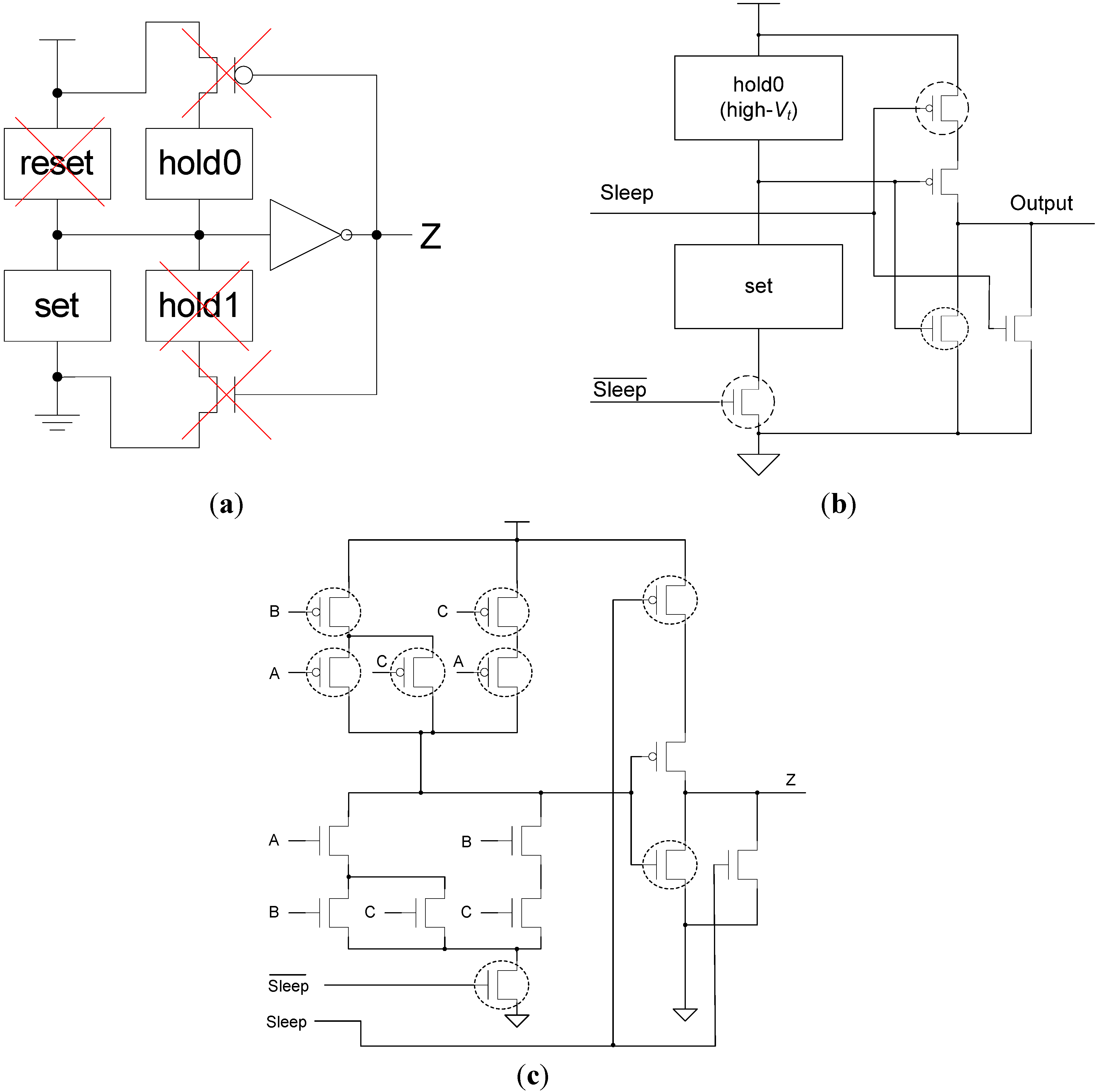
Improved from the direct MTCMOS NCL threshold gate implementation [15], similar to the structure shown in Figure 5, a modified Static MTNCL threshold gate structure, referred to as SMTNCL, is shown in Figure 7b. This modification eliminates the output wake-up glitch by moving the power gating high-Vt transistor to the PDN, and removing the two bypass transistors. All PMOS transistors except the output inverter are high-Vt, because they are only turned on when the gate enters sleep mode and the inputs become logic 0, and remain on when the gate exits sleep mode, until the gate’s set condition becomes true. In both cases, the gate output is already logic 0; therefore, the speed of these PMOS transistors does not affect performance, so high-Vt transistors are used to reduce leakage current. During active mode, the Sleep signal is logic 0 and is logic 1, such that the gate functions as normal. During sleep mode, Sleep is logic 1 and is logic 0, such that the output low-Vt pull-down transistor is turned on quickly to pull the output to logic 0, while the high-Vt NMOS gating transistor is turned off to reduce leakage. Note that since the internal node, between set and hold0, is logic 1 during sleep mode and the output is logic 0, the NMOS transistor in the output inverter is no longer on the critical path and therefore can be a high-Vt transistor. As an example, this SMTNCL implementation of the static TH23 gate is shown in Figure 7c.
2.3.3. MTNCL Threshold Gate Design for ECII Architecture
Combining the ECII architecture with the SMTNCL gate structure, results in a delay-sensitivity problem, as shown in Figure 8. After a DATA cycle, if most, but not all, inputs become NULL, this Partial NULL (PN) wavefront can pass through the stage’s input register, because the subsequent stage is requesting NULL, and cause all stage outputs to become NULL, before all inputs are NULL and the stage is put to sleep, because the hold1 logic has been removed from the SMTNCL gates. This violates the input-completeness criteria, discussed in Section 2.1, and can cause the subsequent stage to request the next DATA while the previous stage input is still a partial NULL, such that the preceding wavefront bits that are still DATA will be retained and utilized in the subsequent operation, thereby compromising delay-insensitivity, similar to the problem when using regular completion instead of Early Completion for MTNCL [18].

Figure 8.
Delay-sensitivity problem combining ECII architecture with SMTNCL gates.
Figure 8.
Delay-sensitivity problem combining ECII architecture with SMTNCL gates.
There are two solutions to this problem, one at the architecture level and the other at the gate level. Since the problem is caused by a partial NULL passing through the register, this can be fixed at the architecture-level by ensuring that the NULL wavefront is only allowed to pass through the register after all register inputs are NULL, which is easily achievable by using the stage’s inverted sleep signal as its input register’s Ki signal. This Fixed Early Completion Input-Incomplete (FECII) architecture is shown in Figure 9. Compared to ECII, FECII is slower because the registers must wait until all inputs become DATA/NULL before they are latched. Note that a partial DATA wavefront passing through the register does not pose a problem, because the stage will remain in sleep mode until all inputs are DATA, thereby ensuring that all stage outputs will remain NULL until all inputs are DATA.
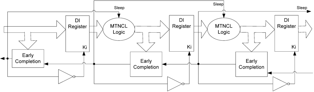
Figure 9.
Fixed Early Completion Input-Incomplete (FECII) architecture.
Figure 9.
Fixed Early Completion Input-Incomplete (FECII) architecture.
This problem can also be solved at the gate level by adding the hold1 logic back into each SMTNCL gate, to ensure input-completeness with respect to NULL, such that a partial NULL wavefront cannot cause all outputs to become NULL. Note that this requires the PMOS transistor between hold0 and VDD to be re-added to prevent a direct path from VDD to ground when both hold1 and hold0 are simultaneously asserted. Also note that the hold1 transistors not shared with the set condition can be high-Vt transistors, since they are not on the critical path. This Static MTNCL implementation with hold1 is shown in Figure 10, and is denoted as SMTNCL1.

Figure 10.
(a) SMTNCL1 gate structure; (b) TH23 implementation.
Figure 10.
(a) SMTNCL1 gate structure; (b) TH23 implementation.
To summarize, the ECII architecture only works with SMTNCL1 gates, which include the hold1 function. The FECII architecture works with both SMTNCL and SMTNCL1 gates; however, SMTNCL gates would normally be used with FECII since they require fewer transistors. Additionally, the ECII architecture is faster than FECII, when both use the same MTNCL gates.
2.3.4. Bit-Wise MTNCL
Bit-Wise MTNCL (BWMTNCL) was developed in [19] to yield an ultra-low power methodology for bit-wise pipelined [7] NCL systems. Direct application of the MTNCL concept (i.e., utilizing Early Completion and sleeping gates in lieu of the NULL cycle) to bit-wise pipelined NCL systems resulted in excessive overhead [19]. So, BWMTNCL instead utilizes the regular NCL architecture, shown in Figure 3, along with the regular NCL gate design, shown in Figure 7a, modified to utilize the minimum number of high-Vt transistors such that all paths from VDD to ground contain a high-Vt transistor. As an example, the BWMTNCL TH23 gate is shown in Figure 11. Even though BWMTNCL was originally developed for bit-wise pipelined NCL systems, the BWMTNCL gates can also be used for full-word pipelined NCL systems, as demonstrated in [19] and included for comparison herein.

Figure 11.
BWMTNCL applied to TH23 gate.
Figure 11.
BWMTNCL applied to TH23 gate.
3. MTNCL Enhancements
The previous SMTNCL1 gate, shown in Figure 10, requires a significant number of additional transistors to implement the hold1 functionality; however, the number of additional transistors can be significantly reduced. Additionally, the previous MTNCL architecture only allows for the combinational logic (C/L) to be slept, whereas this paper develops two modified MTNCL architectures, where (1) the completion logic can also be slept; and (2) both the registration and completion logic can also be slept.
3.1. New SMTNCL1 Gate
Figure 12 shows the new SMTNCL1 gate, which only requires two additional transistors vs. the SMTNCL gate. The difference between the new SMTNCL1 gate in Figure 12 and the previous version in Figure 10 is that the hold1 logic has been removed. The feedback NMOS transistor is sufficient to hold the output at logic 1, without the hold1 circuitry, because this ensures that once the gate output has been asserted due to the current DATA wavefront, that it will only be de-asserted when the gate is put to sleep (i.e., when all circuit inputs are NULL), and will not be de-asserted due to a partial NULL wavefront.

Figure 12.
(a) New SMTNCL1 gate structure; (b) TH23 implementation.
Figure 12.
(a) New SMTNCL1 gate structure; (b) TH23 implementation.
3.2. Sleep Completion and Registration Logic
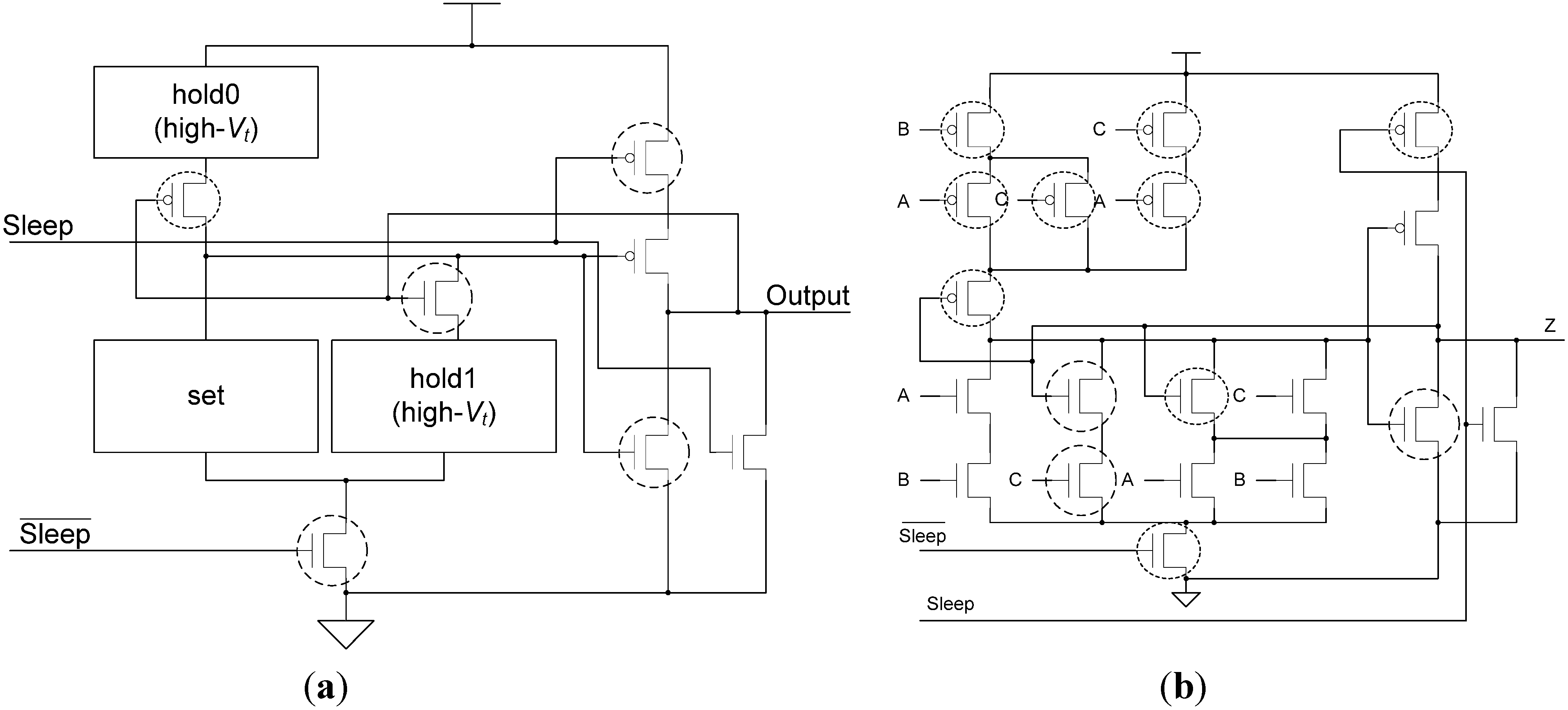
Section 2.3 described the MTNCL architecture where an NCL circuit’s C/L was slept in lieu of the NULL cycle to significantly reduce leakage power. However, during sleep mode the circuit’s completion and registration logic remains active, which for a fine grain pipelined circuit may be a significant portion of the logic. Therefore, it would be very beneficial to be able to sleep the completion and registration logic in addition to the C/L. The completion logic can be slept by modifying the ECII architecture, shown in Figure 6, to include a sleep input to the completion logic and use SMTNCL1 gates to implement the completion logic, as shown in Figure 13 and Figure 14, respectively. Note that the final inverting TH22 gate is a regular NCL gate, which is not slept. This is consistent with the NULL cycle, where the internal completion component gates are all logic 0, except for the final inverting TH22 gate.

Figure 13.
SECII architecture with Completion Logic slept.
Figure 13.
SECII architecture with Completion Logic slept.
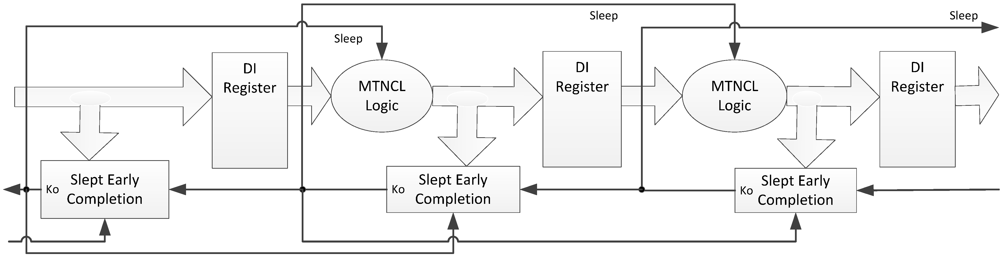
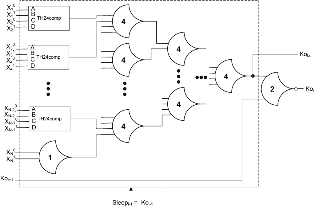
Figure 14.
Early completion component with Sleep input.
Figure 14.
Early completion component with Sleep input.

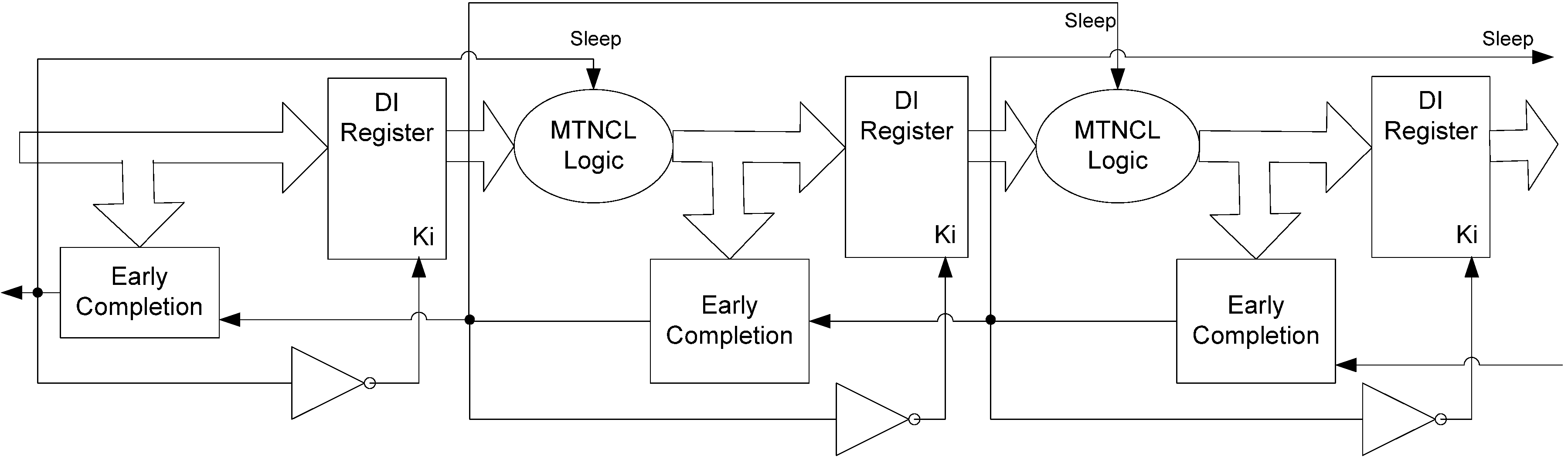
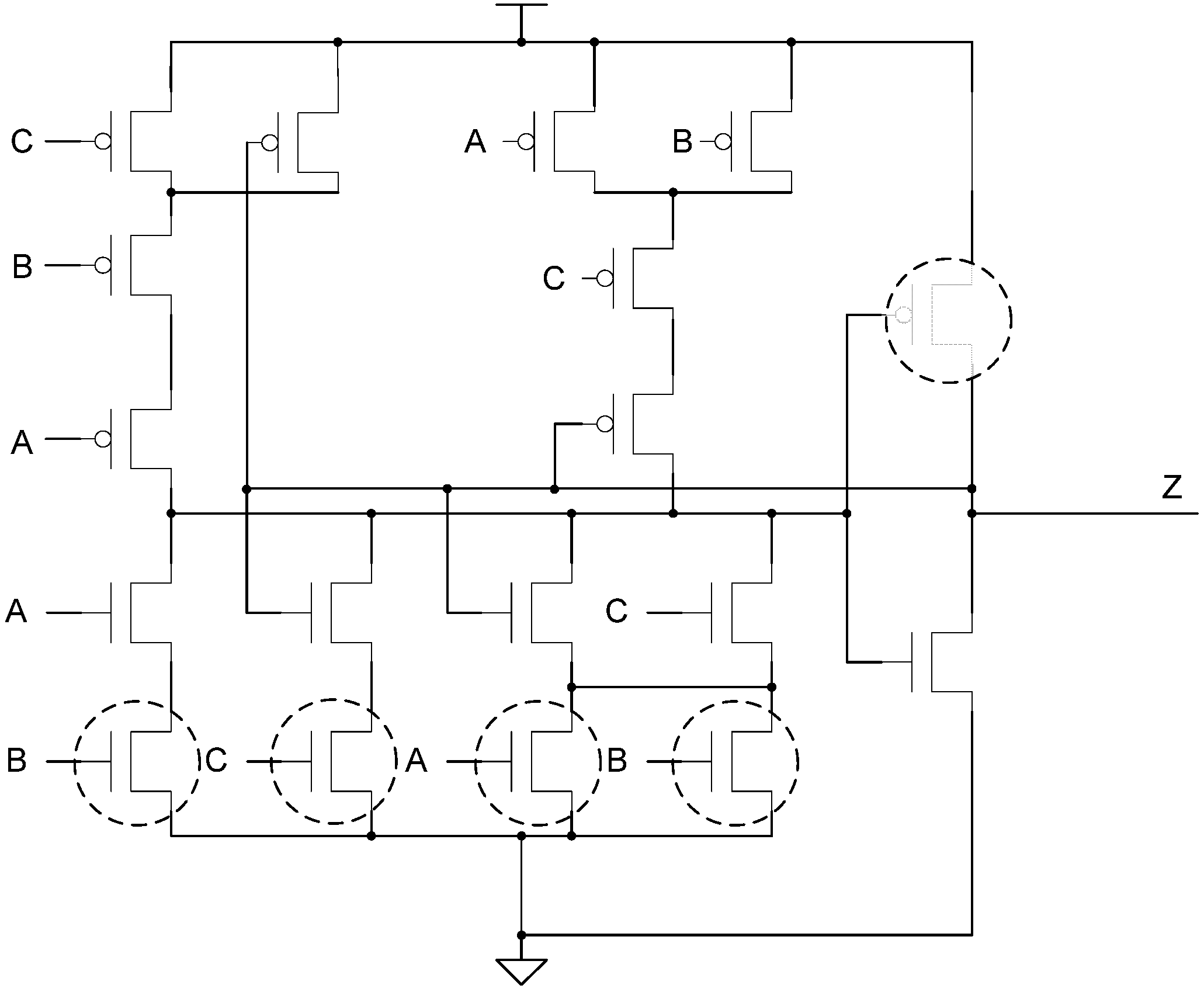
During a NULL cycle, the register output is also NULL, so it too can be slept, as shown in Figure 15. Instead of using two SMTNCL1 TH22 gates to implement the register, the sleep transistors for each rail can be combined, such that a dual-rail register is implemented as a single component in order to reduce the area, as shown in Figure 16a. Note that this architecture is similar to the FECII architecture shown in Figure 9, which does not allow a partial NULL to propagate through the register, such that the C/L can be implemented with the smaller SMTNCL gates instead of SMTNCL1 gates.
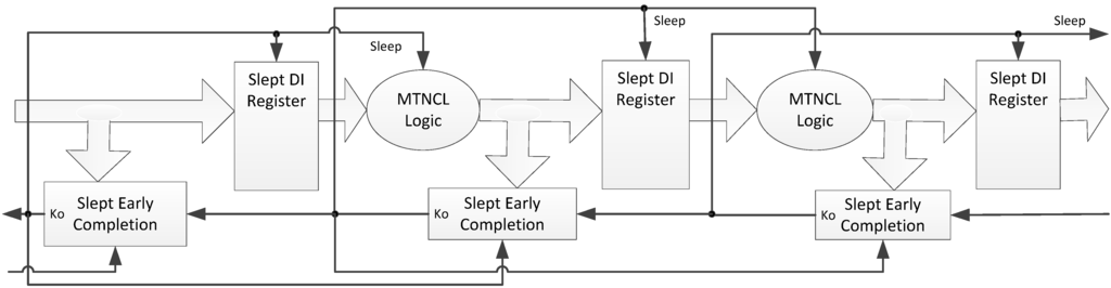
Figure 15.
SECRII architecture with Completion Logic and Registration slept.
Figure 15.
SECRII architecture with Completion Logic and Registration slept.

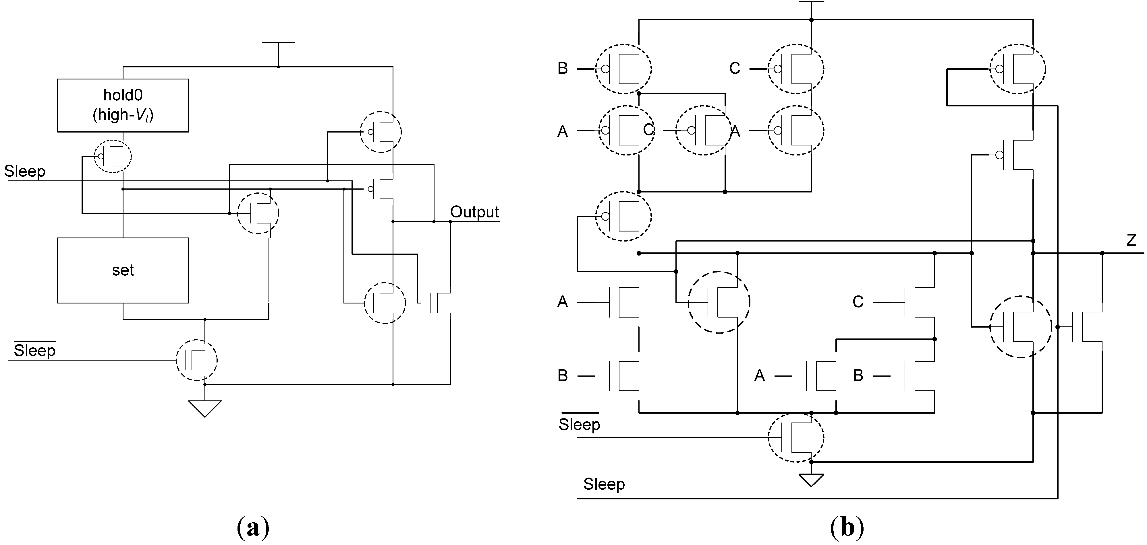
3.3. Combine SECRII with BWMTNCL
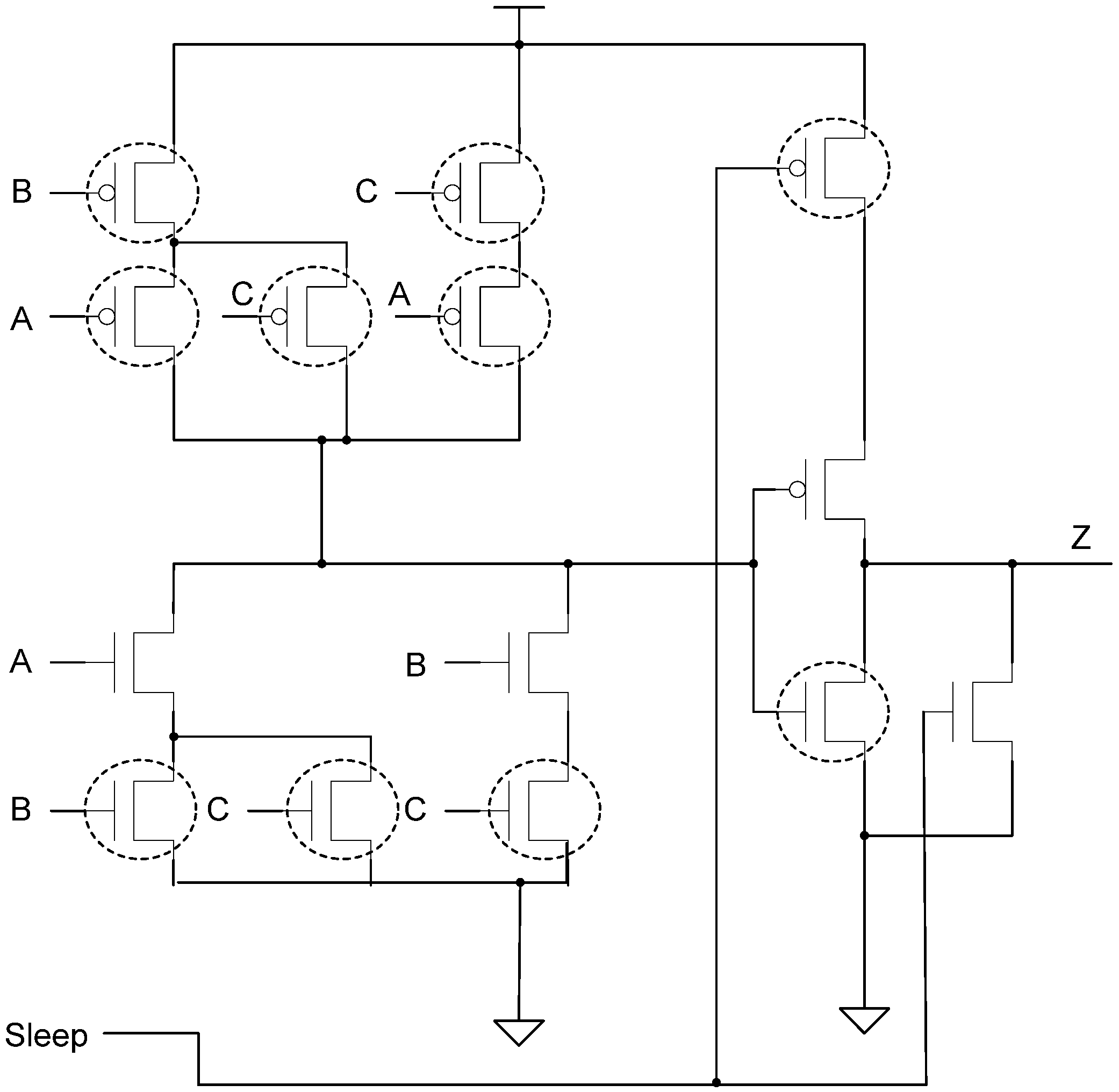
The SMTNCL gates utilized in the SECRII architecture require both a Sleep and input, each of which necessitates a large buffer tree. Hence, eliminating one of these inputs would decrease area and energy. The (nsleep), input can be eliminated from the SMTNCL gate by combining the SMTNCL architecture in Figure 7 with the BWMTNCL architecture in Figure 11, as shown in Figure 16b and Figure 17. Instead of utilizing a high-Vt transistor to gate the set logic from ground, the set logic is implemented in BWMTNCL fashion utilizing the minimum number of high-Vt transistors such that all paths through the set function to ground contain a high-Vt transistor.

Figure 16.
Slept DI register: (a) with both Sleep and nsleep inputs; (b) w/o nsleep input.
Figure 16.
Slept DI register: (a) with both Sleep and nsleep inputs; (b) w/o nsleep input.
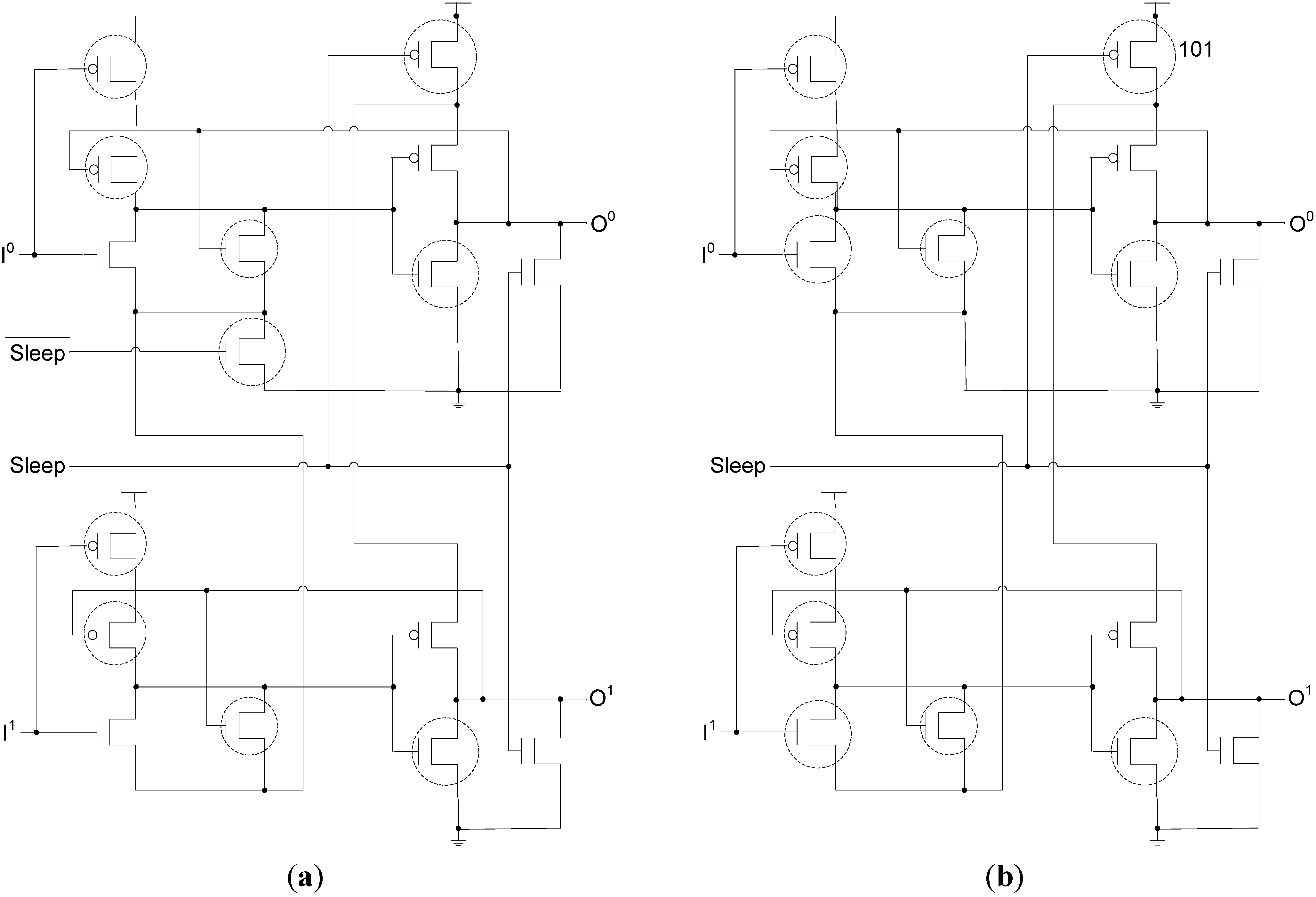

Figure 17.
SMTNCL w/o nsleep applied to TH23 gate.
Figure 17.
SMTNCL w/o nsleep applied to TH23 gate.
3.4. Safe SECRII Architecture
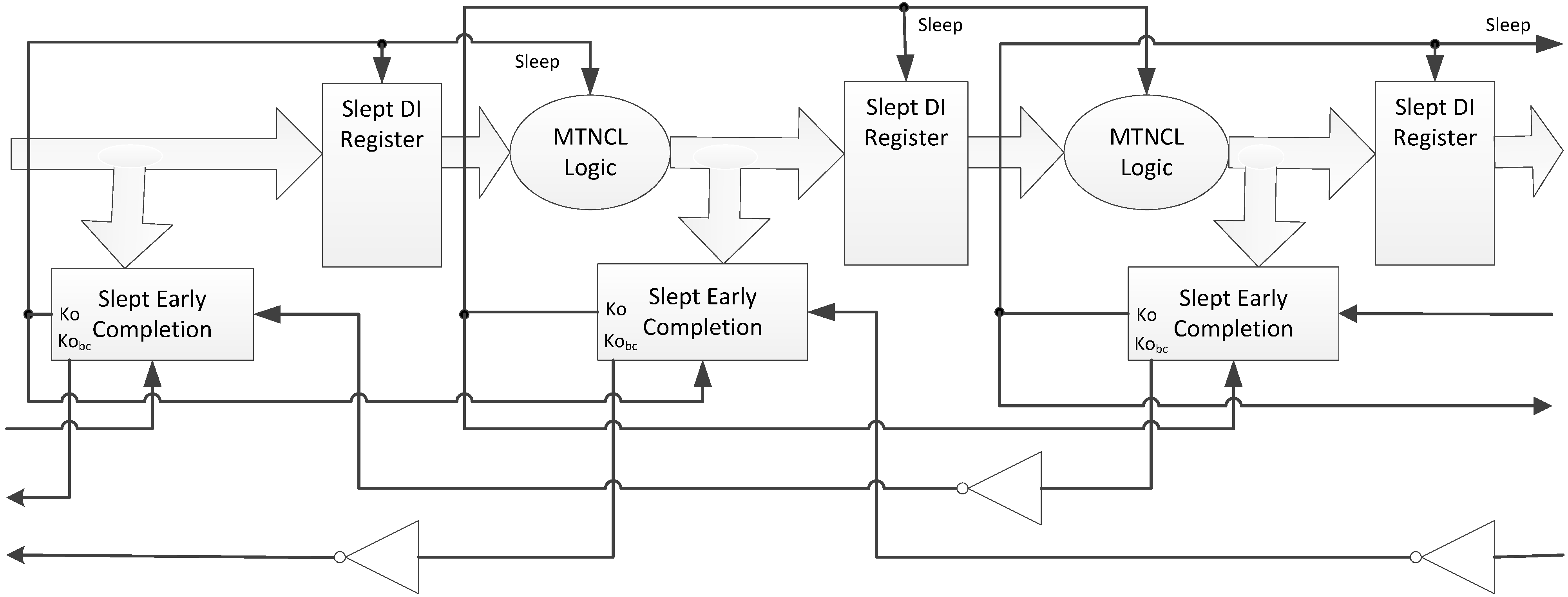
The SECRII w/o nsleep architecture pushes the benefits of MTNCL to its limits, providing for the smallest, fastest, and lowest energy consuming MTNCL architecture, as discussed in Section 4. The SECRII architecture, however, comes with more timing sensitivity due to a potential race condition between sleeping a stage and latching DATA for the next stage. For example, when registeri’s input is DATA, and DATA is being requested by the next stage, registeri’s Slept Early Completion component output will change from logic 1 to logic 0, which will wake up registeri to latch the DATA. If the input to the previous register, registeri−1, is already NULL, the 1 to 0 transition of registeri’s Slept Early Completion component will cause registeri−1’s Slept Early Completion component output to change from logic 0 to logic 1, which will sleep the C/L preceding registeri. Hence, a race condition exists between registeri latching the DATA before it becomes NULL by sleeping the preceding C/L that generated the DATA, such that the time to pass DATA through registeri once its sleep input transitions from 1 to 0 must be less than the time to transition registeri−1’s Slept Early Completion component inverting TH22 output gate from 0 to 1 followed by the time to sleep the C/L preceding registeri to NULL. The first path is a single MTNCL gate (the register); whereas the second path consists of an NCL TH22 gate, followed by an inverter, followed by an MTNCL gate; therefore, this potential race condition is easily mitigated. Note that in practice, both of these paths also contain a buffer tree for the sleep signal; hence, a simple analysis of each sleep network is needed to ensure that its timing is not generating a problematic race condition.
This potentially problematic race condition can be avoided by using the safe SECRII architecture, as described in [21] and shown in Figure 18. This safe architecture requires the DATA wavefront to completely propagate through the next stage before sleeping the current stage, hence, avoiding the race condition. This can be easily achieved by using the signal at the output of the completion tree (before the final inverting TH22 gate, referred to as Kobc in Figure 14) of the next stage as the Ko input to the Early Completion/Sleep Generation circuit for the current stage. This signal is shown as an additional output for each Early Completion component in Figure 18, and must be inverted before connecting to the Ko input of the previous Early Completion component. The main drawback of this safe architecture is that it significantly decreases performance.

Figure 18.
Safe SECRII architecture.
Figure 18.
Safe SECRII architecture.
4. Simulation Results
To compare the various MTNCL architectures, a number of four-stage pipelined 32-bit IEEE single-precision floating-point co-processors, which perform addition, subtraction, and multiplication [22], as shown in Figure 19, were designed using the 1.2V IBM 8RF-LM 130 nm CMOS process, and were simulated at the transistor level, after inserting buffers, using Cadence’s UltraSim simulator running a VerilogA controller in mixed-signal mode that utilized 25 sets of randomly selected floating-point numbers for each add/sub and multiply operation, whose results were averaged to generate the data shown in Table 1. Note that all transistors for all designs, both asynchronous and synchronous, are minimum sized except for the buffers. Table 1 lists the MTNCL results and also compares to the regular NCL implementation using all low-Vt transistors and all high-Vt transistors, and the synchronous MTCMOS design. Note that the synchronous MTCMOS design only sleeps after a preset number of identical input datasets are received, which requires a small Power Management Unit (PMU) to compare adjacent datasets and count identical consecutive datasets [23]. The floating-point co-processor has two distinct datapaths, the add/subtract unit and the multiplier, which have different throughput, so the data for each is presented separately, and can be averaged to yield the combined results. TDD is the average DATA plus NULL processing time, which is comparable to the synchronous clock period. To compare to the MTCMOS synchronous design, the clock was set to match the speed of the fastest MTNCL design, even though the synchronous design can operate faster (less than 2X). TDD and Energy/Operation are calculated while the circuit is operating at its maximum speed, while Idle Power is calculated using DC analysis after the pipeline is flushed with all NULL inputs for the asynchronous circuits, and after the PMU sleeps the synchronous circuit. Note that the PMU must always stay active and can never sleep because it needs to continuously monitor the incoming data to know when it changes in order to wake up the rest of the circuitry to process the new data. Hence, for the asynchronous circuits, idle power is equivalent to leakage power, and does not depend on the previous type of operations (i.e., either add/sub or mult), since the following sleep state is the same (i.e., both pipelines are all NULL). However, idle power is slightly different for add/sub vs. mult for the synchronous design because the clock period is different.
Comparing the various MTNCL designs shows that the new MTNCL gate with hold1 (SMTNCL1) requires less area, energy, and power than the previous version in [18], and is slightly faster. Sleeping the completion logic along with the C/L slightly reduces area, energy, and leakage power, and significantly increases speed, while sleeping the C/L, completion logic, and registers significantly decreases area, energy, and leakage power, and slightly increases speed. The SMTNCL with SECRII without nsleep design that combines the SMTNCL with SECRII and BWMTNCL architectures further reduces area and energy while increasing speed, at the cost of a slight increase in leakage power. Note that the FECII circuit is faster than the ECII circuit because the FECII design utilizes the faster SMTNCL gates.

Figure 19.
Thirty-two-bit IEEE single-precision floating-point co-processor architecture.
Figure 19.
Thirty-two-bit IEEE single-precision floating-point co-processor architecture.
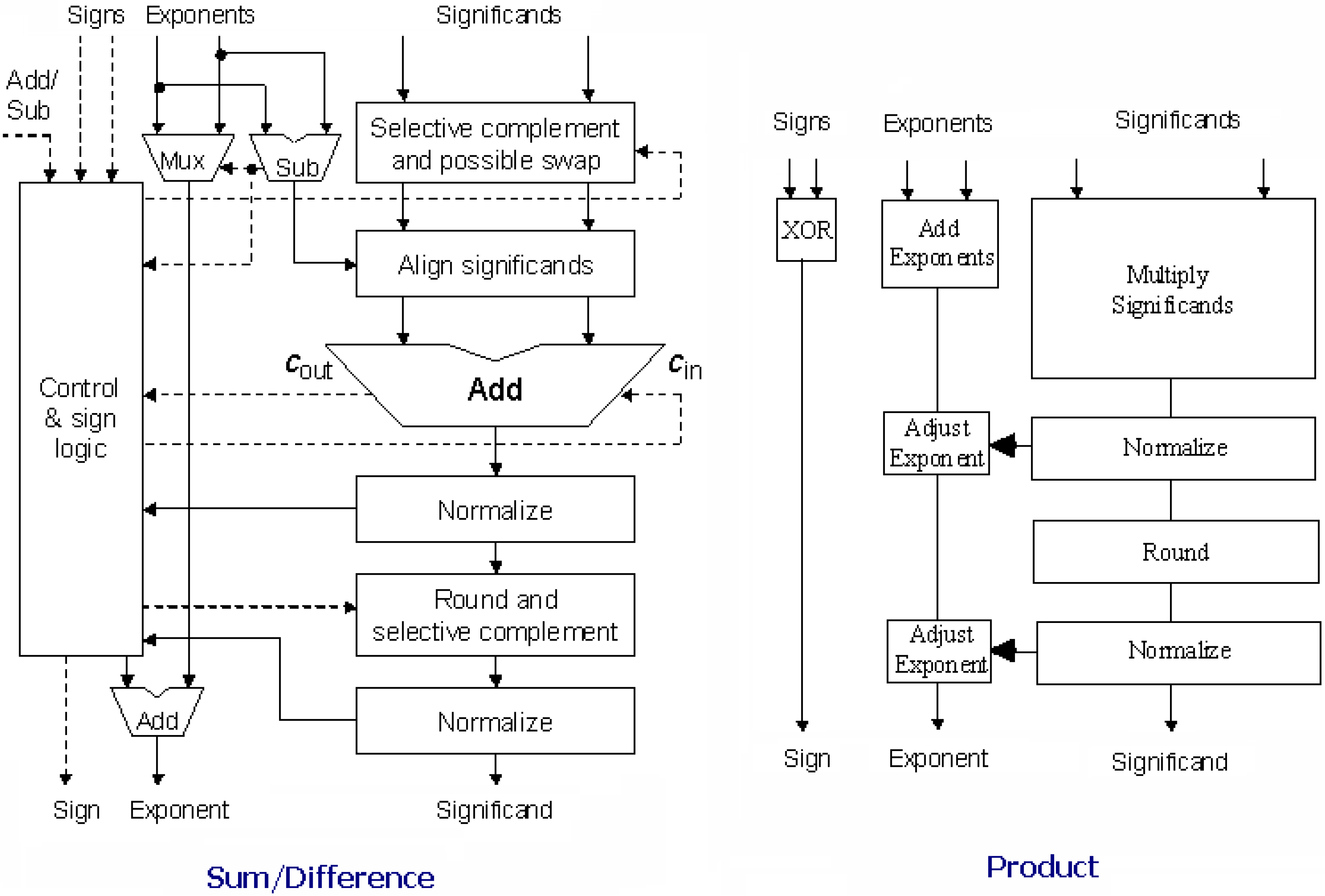

Table 1.
MTNCL comparisons.
| Circuit Type | # Transistors | TDD (ns) | Energy/Operation (pJ) | Idle Power (nW) | |||
|---|---|---|---|---|---|---|---|
| add/sub. | Mult. | add/sub. | Mult. | add/sub. | Mult. | ||
| NCL Low-Vt | 158059 | 14.1 | 14.4 | 27.4 | 23.7 | 12,300 | 12,300 |
| NCL High-Vt | 158059 | 32.7 | 33.4 | 28.5 | 25.1 | 208.0 | 208.0 |
| BWMTNCL | 158059 | 17.9 | 16.2 | 27.1 | 23.7 | 190.7 | 190.7 |
| SMTCNL with FECII | 111506 | 11.6 | 15.3 | 14.9 | 27.5 | 115.9 | 115.9 |
| Original SMTNCL1 with ECII | 130476 | 12.5 | 16.7 | 16.0 | 27.8 | 140.8 | 140.8 |
| New SMTNCL1 with ECII | 119706 | 12.1 | 15.7 | 14.7 | 26.1 | 121.9 | 121.9 |
| SMTNCL1 with SECII | 119244 | 10.7 | 15.4 | 14.6 | 26.0 | 121.1 | 121.1 |
| SMTNCL with SECRII | 96640 | 11.1 | 14.8 | 13.5 | 25.3 | 111.2 | 111.2 |
| SMTNCL with SECRII w/o nsleep | 90041 | 10.0 | 13.9 | 12.1 | 21.8 | 112.1 | 112.1 |
| SMTNCL with SECRII w/o nsleep (safe architecture) | 90049 | 13.4 | 16.6 | 12.3 | 22.3 | 113 | 113 |
| MTCMOS Synchronous | 104571 | 10.0 | 13.9 | 124.3 | 124.7 | 156,000 | 132,000 |
The best MTNCL design, SMTNCL with SECRII without nsleep, requires 43% less area, 34% less energy, two orders of magnitude less leakage power, and is 19% faster than the regular low-Vt NCL design, has 46% less leakage power than the regular high-Vt NCL design, and requires 14% less area, 86% less energy, and three orders of magnitude less idle power than the synchronous MTCMOS design while operating at the same speed, although the MTCMOS synchronous design can operate faster (less than 2X). Note that the synchronous circuit’s idle power is mostly dynamic power from its PMU, which continues to run when the co-processor is idle to determine when to wake up the co-processor, as mentioned above, which is why it is so much more than the asynchronous designs, which due to their handshaking, do not switch at all when idle, without requiring any additional circuitry. Hence, if a user-controlled sleep input was added, the synchronous circuit would not require a PMU, such that its idle power would be solely comprised of its leakage power, which would be the same order of magnitude as the MTNCL asynchronous designs, since leakage power is proportional to number of gates for MTCMOS based circuits.
Hence, the SMTNCL with SECRII without nsleep architecture presented herein vastly outperforms traditional NCL in all aspects, area, speed, energy, and leakage power, and significantly outperforms the MTCMOS synchronous architecture in terms of area, energy, and idle power. Finally, to increase timing robustness, one can optionally use the safe SMTNCL with SECRII without nsleep architecture, which preserves all the area and power advantages of the normal SMTNCL with SECRII without nsleep architecture but reduces performance.
5. Conclusions
This paper describes enhancements to the ultra-low power MTNCL methodology developed in [15,16,17,18,19]. Specifically, a new MTNCL gate with hold1 capability was designed, which is smaller, faster, and has lower power than the previous version in [18]. Additionally, two new MTNCL architectures were developed that allow for the completion logic to be slept in addition to the C/L and for the C/L, completion logic, and registration to all be slept; and this new architecture was combined with the BWMTNCL architecture in [19] to further reduce area and energy and increase speed by removing the buffer tree. Transistor-level simulation of a four-stage pipelined 32-bit IEEE single-precision floating-point co-processor using the 1.2V IBM 8RF-LM 130 nm CMOS process shows that the new architecture that sleeps the C/L, completion logic, and registration without the buffer tree is superior to the previous MTNCL architectures in all categories (i.e., area, speed, energy, and leakage power), vastly outperforms traditional NCL in all aspects, and significantly outperforms the MTCMOS synchronous architecture in terms of area, energy, and idle power, although the MTCMOS synchronous design can operate faster.
Acknowledgments
The authors gratefully acknowledge the support from DARPA under grant: W15P7T-08-C-V404, and from the National Science Foundation under grant: CCF-1116405.
Author Contributions
Liang Zhou, Scott Smith, and Jia Di developed the MTNCL methodology presented herein; Ravi Parameswaran developed the 32-bit single precision floating-point unit architecture utilized as the test bed herein to compare the various circuits; and Farhad Parsan implemented and simulated the safe SECRII architecture, and wrote the corresponding section.
Conflicts of Interest
The authors declare no conflict of interest.
References
- Mutoh, S.; Douseki, T.; Matsuya, Y.; Aoki, T.; Shigematsu, S.; Yamada, J. 1-V Power Supply High-Speed Digital Circuit Technology with Multithreshold-Voltage CMOS. IEEE J. Solid-State Circuits 1995, 30, 847–854. [Google Scholar] [CrossRef]
- Fant, K.M.; Brandt, S.A. NULL Convention Logic: A Complete and Consistent Logic for Asynchronous Digital Circuit Synthesis. In Proceedings of the International Conference on Application Specific Systems, Architectures and Processors, Chicago, IL, USA, 19–21 August 1996; pp. 261–273.
- Sobelman, G.E.; Fant, K.M. CMOS Circuit Design of Threshold Gates with Hysteresis. In Proceedings of the 1998 IEEE International Symposium on Circuits and Systems (II), Monterey, CA, USA, 31 May–3 June 1998; pp. 61–65.
- Muller, D.E. Asynchronous Logics and Application to Information Processing. In Switching Theory in Space Technology; Stanford University Press: Redwood City, CA, USA, 1963; pp. 289–297. [Google Scholar]
- Parsan, F.A.; Smith, S.C. CMOS Implementation of Static Threshold Gates with Hysteresis: A New Approach. In Proceedings of the IFIP/IEEE International Conference on VLSI-SoC, Santa Cruz, CA, USA, 7–10 October 2012; pp. 41–45.
- Parsan, F.A.; Smith, S.C. CMOS Implementation Comparison of NCL Gates. In Proceedings of the IEEE International Midwest Symposium on Circuits and Systems, Boise, ID, USA, 5–8 August 2012; pp. 394–397.
- Smith, S.C.; DeMara, R.F.; Yuan, J.S.; Hagedorn, M.; Ferguson, D. Delay-Insensitive Gate-Level Pipelining. Elsevier’s Integ. VLSI J. 2001, 30, 103–131. [Google Scholar] [CrossRef]
- Smith, S.C.; DeMara, R.F.; Yuan, J.S.; Ferguson, D.; Lamb, D. Optimization of NULL Convention Self-Timed Circuits. Integr. VLSI J. 2004, 37, 135–165. [Google Scholar] [CrossRef]
- Seitz, C.L. System Timing. In Introduction to VLSI Systems; Addison-Wesley: Boston, MA, USA, 1980; pp. 218–262. [Google Scholar]
- Kondratyev, A.; Neukom, L.; Roig, O.; Taubin, A.; Fant, K. Checking Delay-Insensitivity: 104 Gates and Beyond. In Proceedings of the Eighth International Symposium on Asynchronous Circuits and Systems, Manchester, UK, 8–11 April 2002; pp. 149–157.
- Martin, A.J. Programming in VLSI: From Communicating Processes to Delay-Insensitive Circuits. In Developments in Concurrency and Communication; UT Year of Programming Institute on Concurrent Programming, Addison-Wesley: Boston, MA, USA, 1990; pp. 1–64. [Google Scholar]
- Van Berkel, K. Beware the Isochronic Fork. Integr. VLSI J. 1992, 13, 103–128. [Google Scholar] [CrossRef]
- Kao, J.T.; Chandrakasan, A.P. Dual-Threshold Voltage Techniques for Low-Power Digital Circuits. IEEE J. Solid-State Circuits 2000, 35, 1009–1018. [Google Scholar] [CrossRef]
- Lakshmikanthan, P.; Sahni, K.; Nunez, A. Design of Ultra-Low Power Combinational Standard Library Cells Using a Novel Leakage Reduction Methodology. In Proceedings of the IEEE International SoC Conference, Taipei, Taiwan, 24–27 September 2006; pp. 93–94.
- Bailey, A.D.; Di, J.; Smith, S.C.; Mantooth, H.A. Ultra-Low Power Delay-Insensitive Circuit Design. In Proceedings of IEEE Midwest Symposium on Circuits and Systems, Knoxville, TN, USA, 10–13 August 2008; pp. 503–506.
- Bailey, A.D.; Al Zahrani, A.; Fu, G.; Di, J.; Smith, S.C. Multi-Threshold Asynchronous Circuit Design for Ultra-Low Power. J. Low Power Electron. 2008, 4, 337–348. [Google Scholar] [CrossRef]
- Alzahrani, A.; Bailey, A.D.; Fu, G.; Di, J. Glitch-Free Design for Multi-Threshold CMOS NCL Circuits. In Proceedings of the ACM 2009 Great Lakes Symposium on VLSI, Boston, MA, USA, 10–12 May 2009.
- Smith, S.C.; Di, J. Designing Asynchronous Circuits using NULL Convention Logic (NCL); Synthesis Lectures on Digital Circuits and Systems; Morgan & Claypool Publishers: San Rafael, CA, USA, 2009; Volume 4. [Google Scholar] [CrossRef]
- Zhou, L.; Smith, S.C.; Di, J. An Ultra-Low Power Bit-Wise MTNCL: An Ultra-Low Power Bit-Wise Pipelined Asynchronous Circuit Design Methodology. In Proceedings of the IEEE Midwest Symposium on Circuits and Systems, Seattle, WA, USA, 1–4 August 2010; pp. 217–220.
- Smith, S.C. Speedup of Self-Timed Digital Systems Using Early Completion. In Proceedings of the IEEE Computer Society Annual Symposium on VLSI, Pittsburgh, PA, USA, 25–26 April 2002; pp. 107–113.
- Reese, R.B. UNCLE User Manual. Available online: http://www.ece.msstate.edu/~reese/uncle/UNCLE.pdf (accessed on April 2015).
- Parhami, B. Computer Arithmetic Algorithms and Hardware Designs; Oxford University Press: New York, NY, USA, 2000. [Google Scholar]
- Thian, R. Multi-Threshold CMOS Circuit Design Methodology from 2D to 3D. Master’s Thesis, Computer Science and Computer Engineering Department, University of Arkansas, Fayetteville, AR, USA, December 2010. [Google Scholar]
© 2015 by the authors; licensee MDPI, Basel, Switzerland. This article is an open access article distributed under the terms and conditions of the Creative Commons Attribution license (http://creativecommons.org/licenses/by/4.0/).