An Improved CMOS Design of Op-Amp Comparator with Gain Boosting Technique for Data Converter Circuits


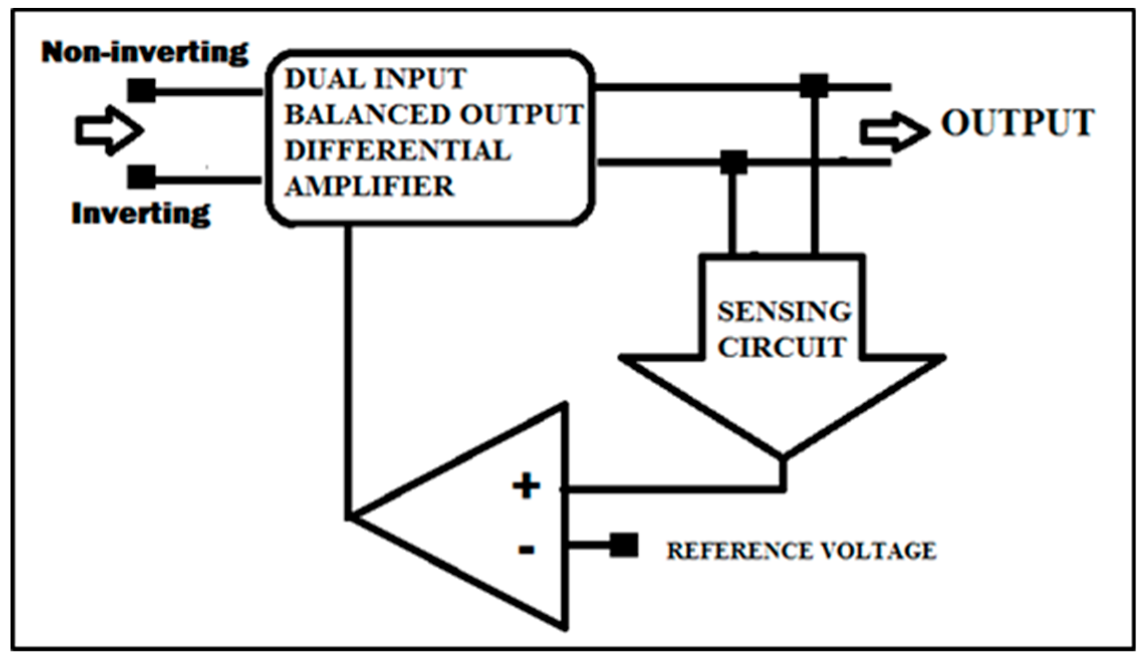
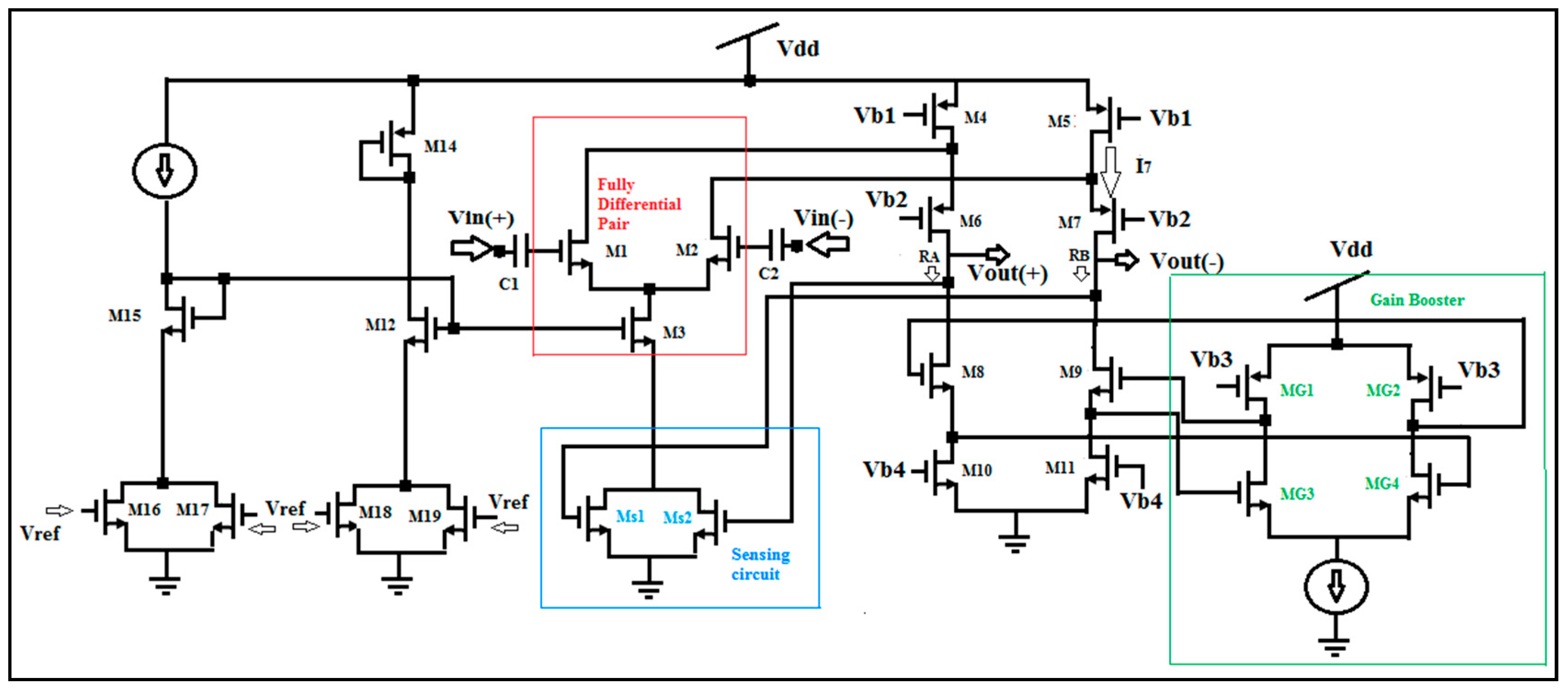
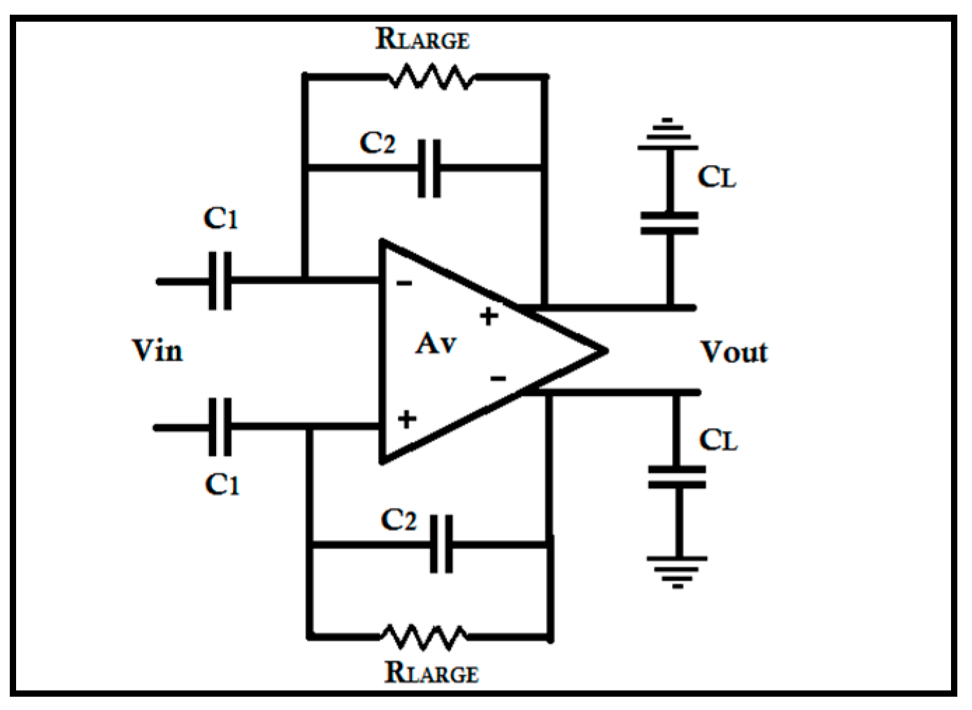
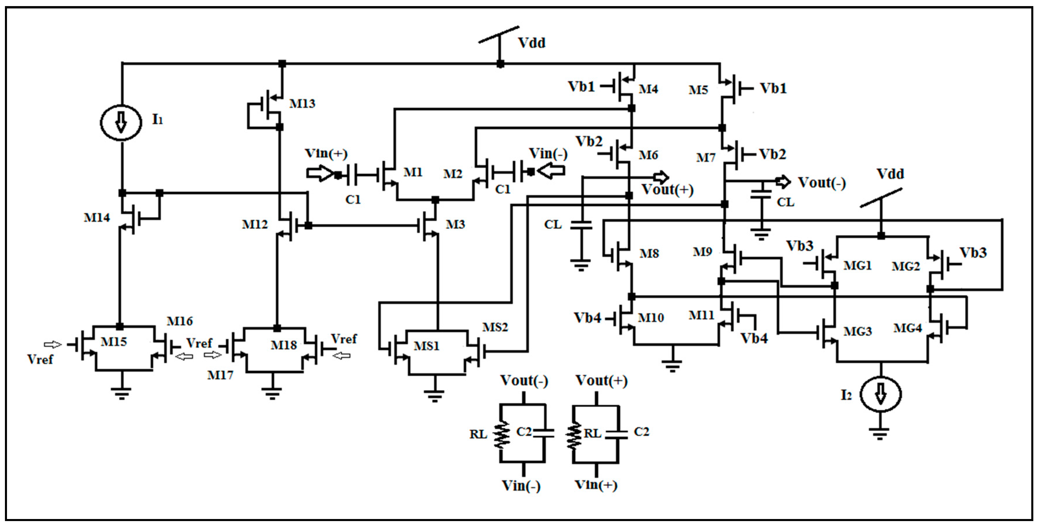
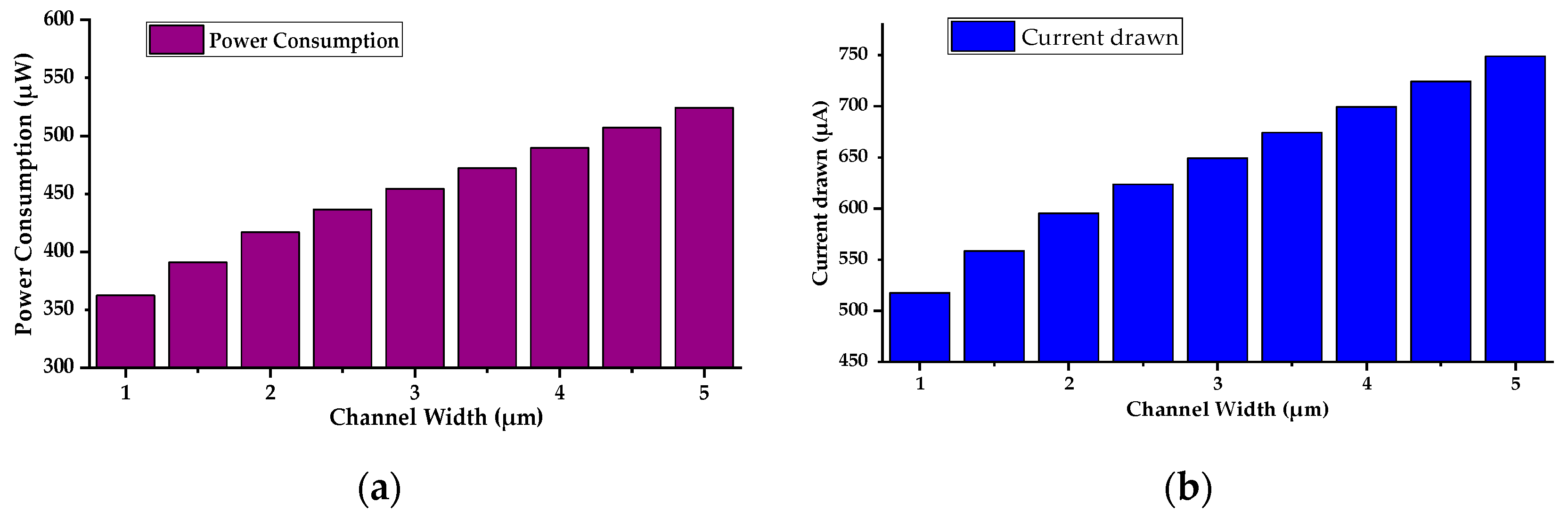
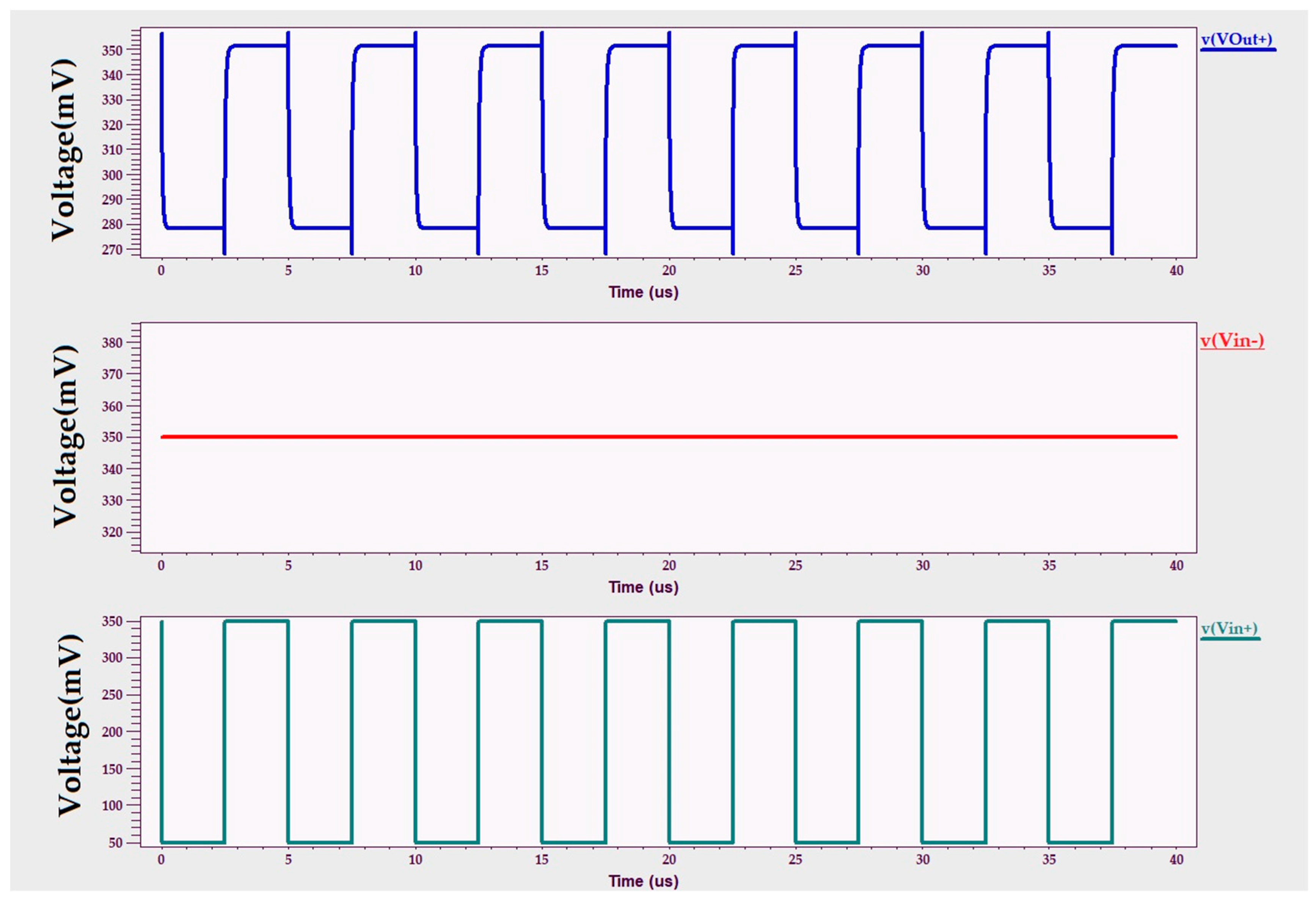
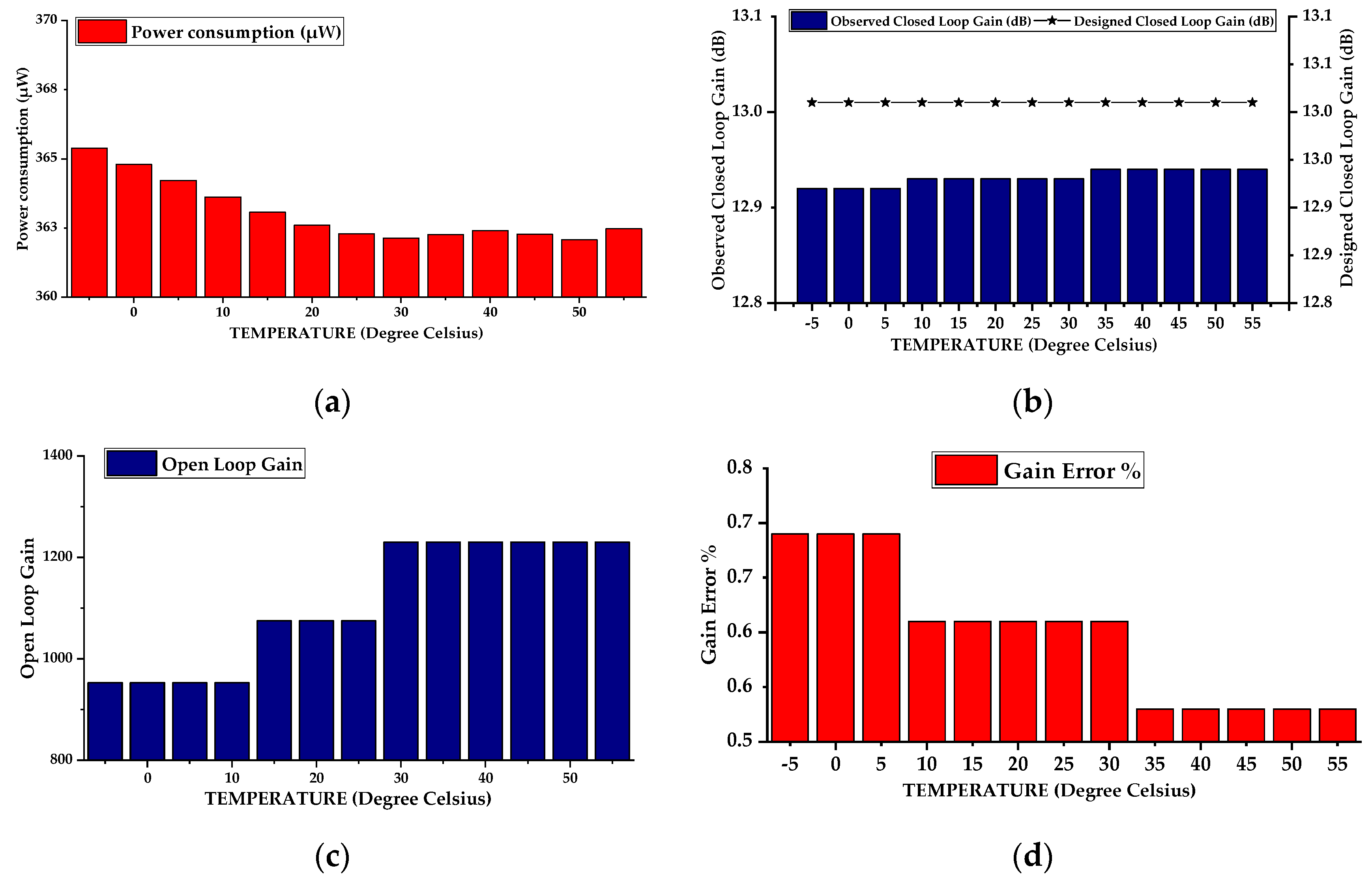
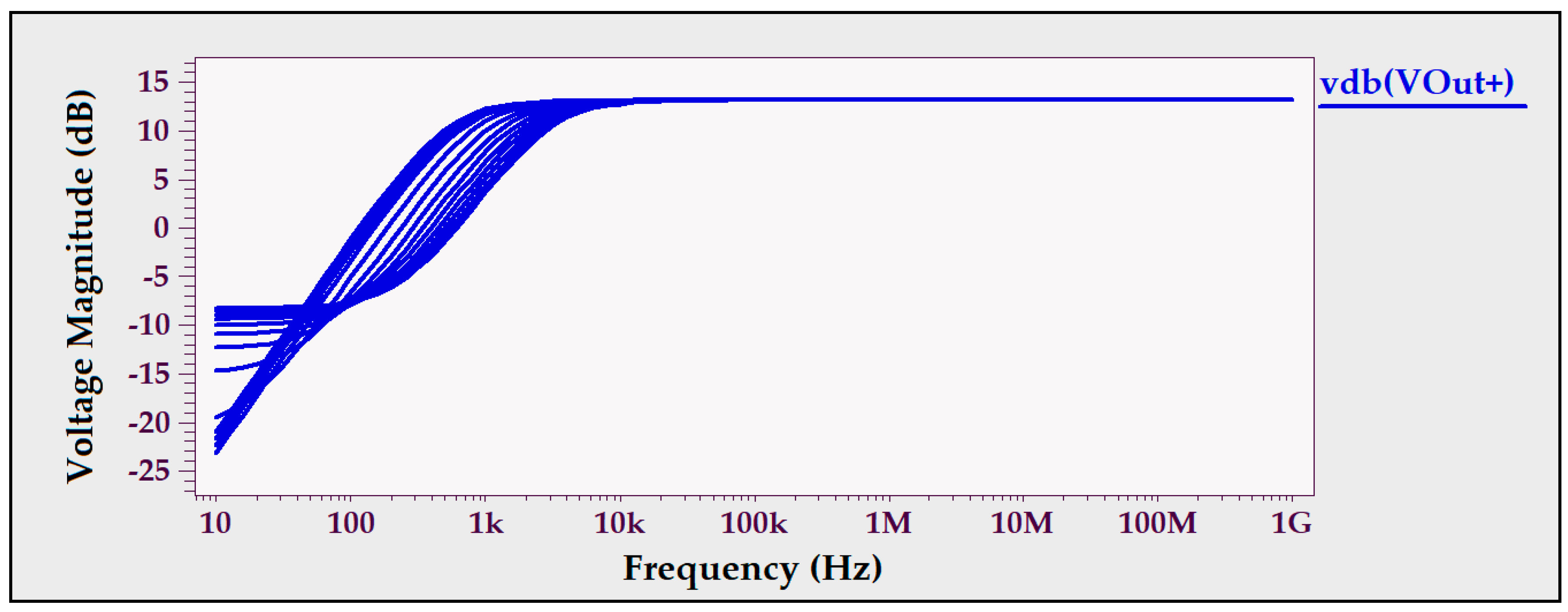
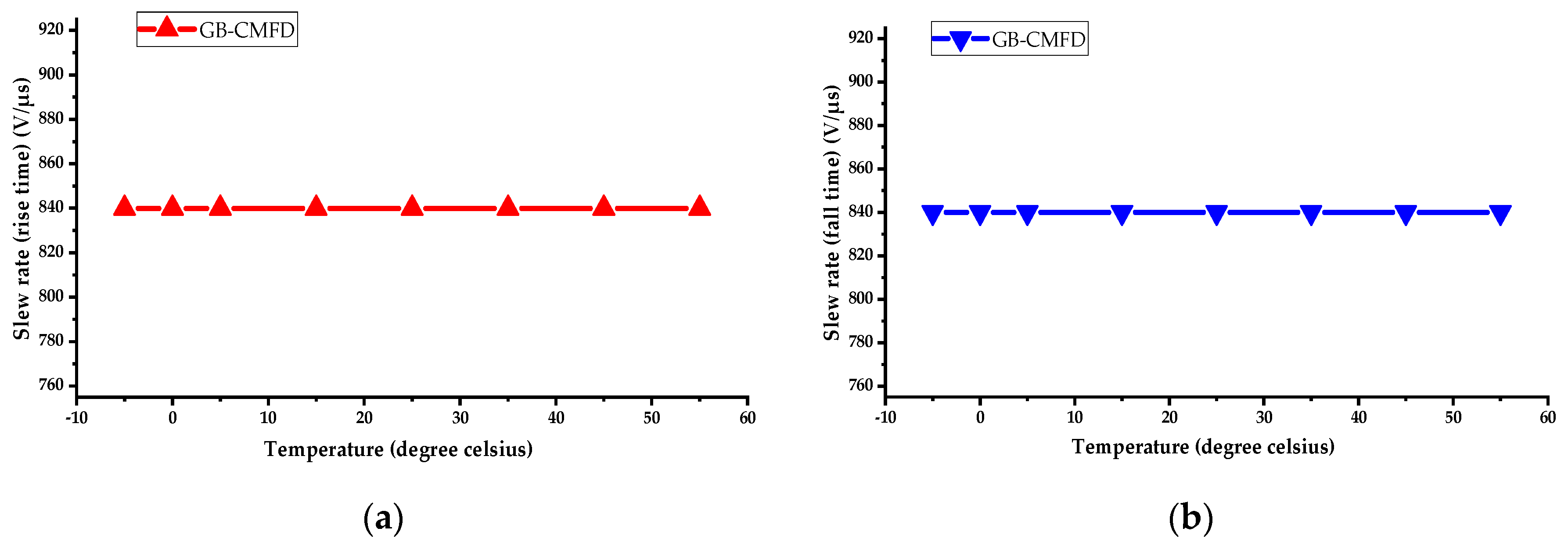
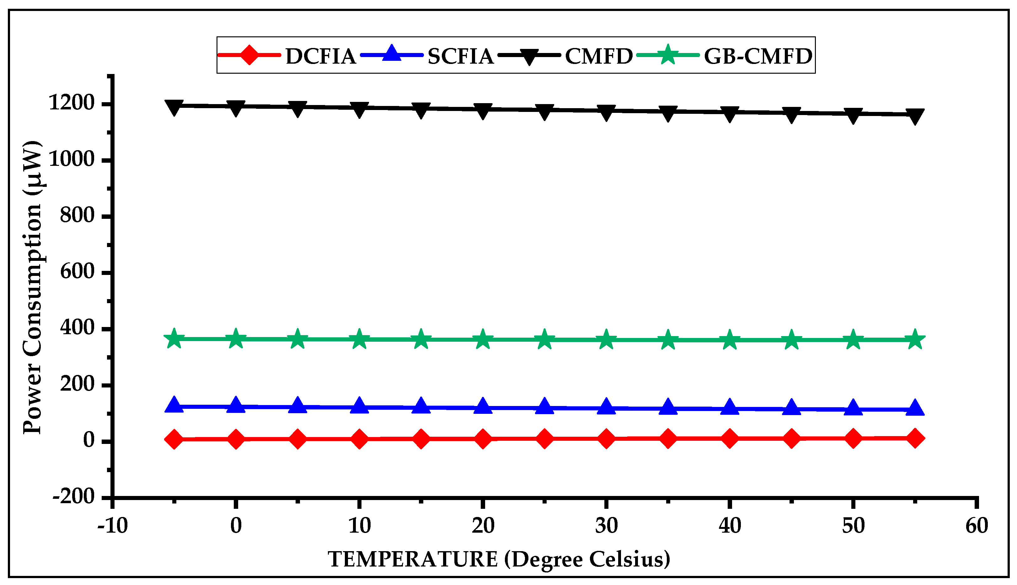
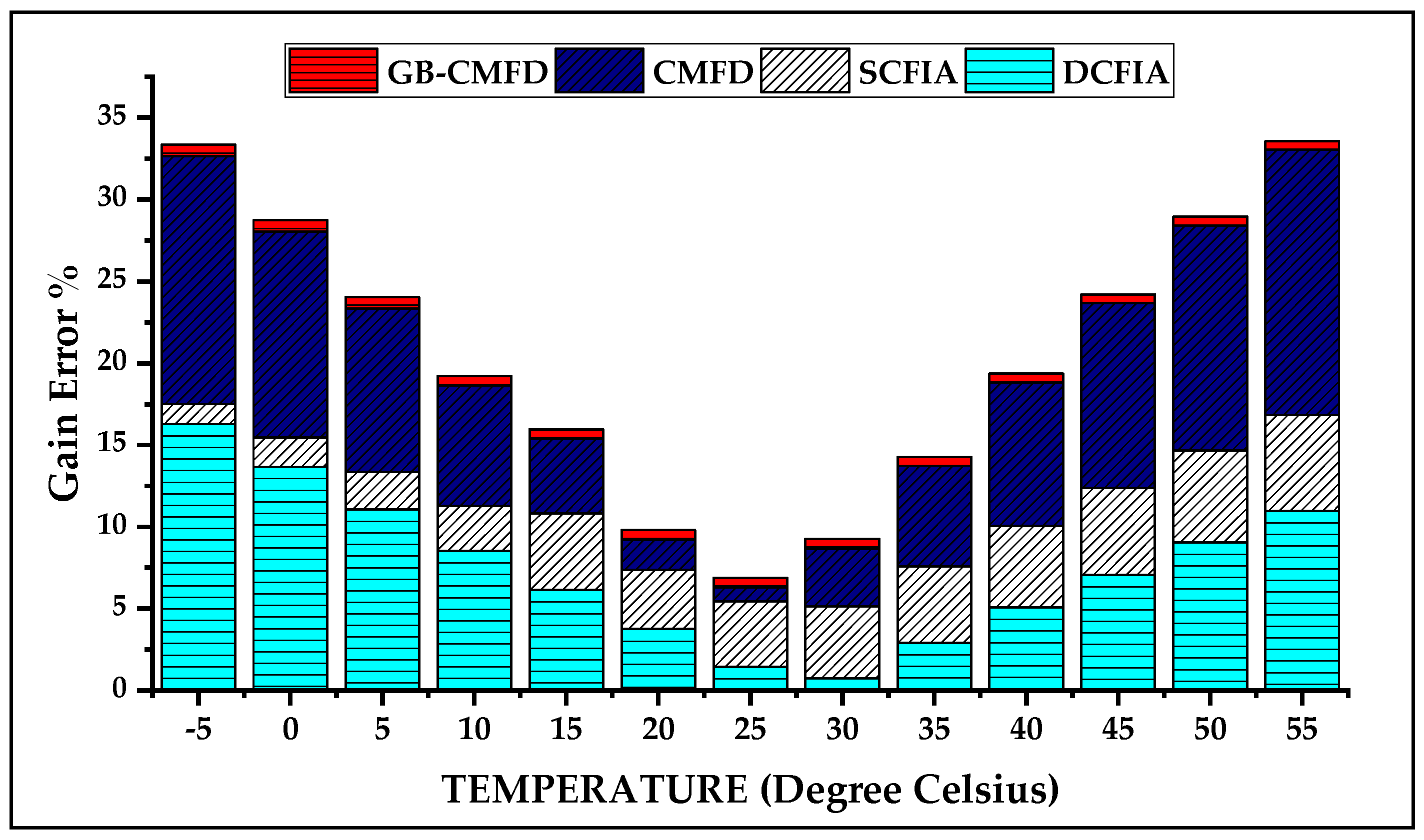
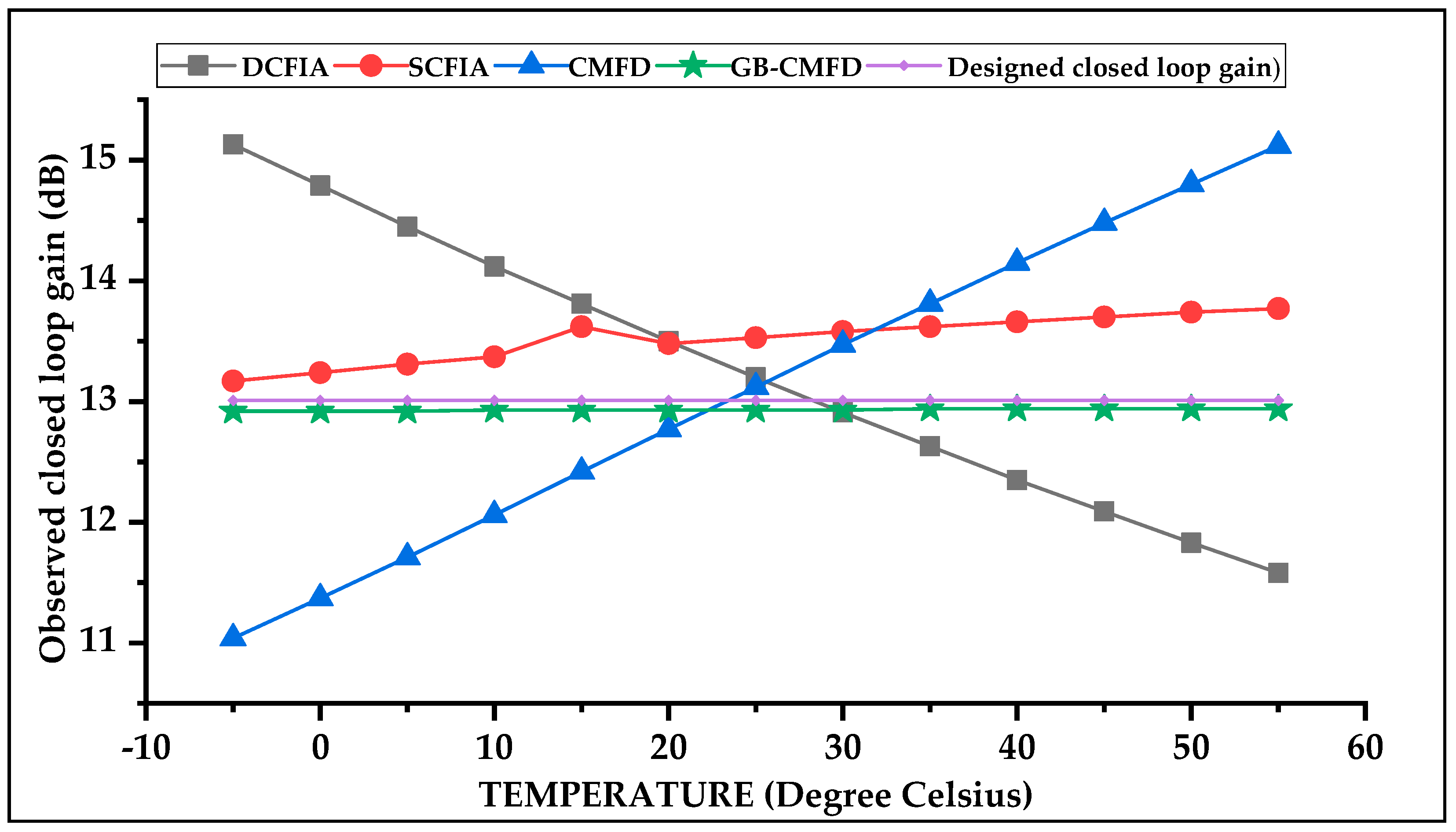
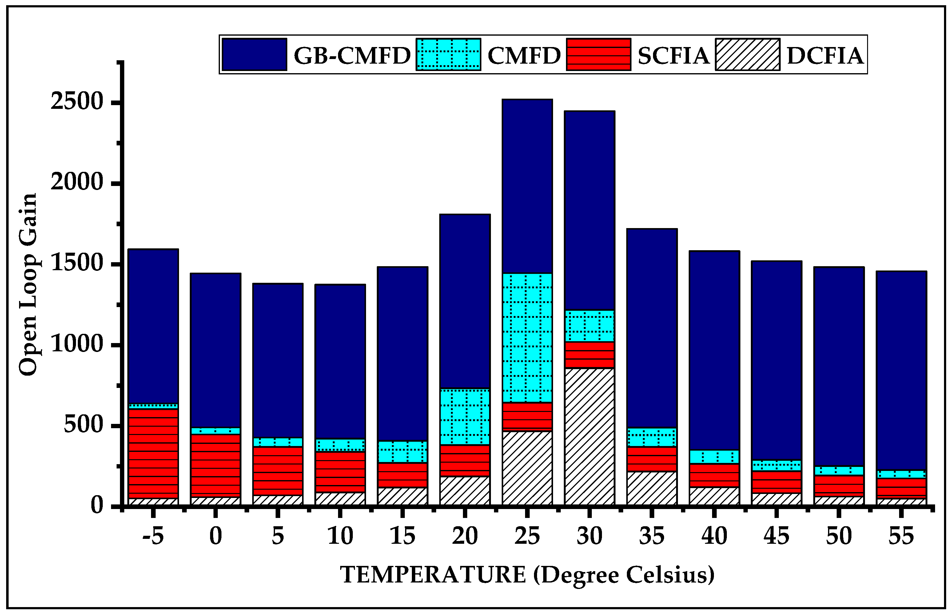
Abstract
Share and Cite
Khatak, A.; Kumar, M.; Dhull, S. An Improved CMOS Design of Op-Amp Comparator with Gain Boosting Technique for Data Converter Circuits. J. Low Power Electron. Appl. 2018, 8, 33. https://doi.org/10.3390/jlpea8040033
Khatak A, Kumar M, Dhull S. An Improved CMOS Design of Op-Amp Comparator with Gain Boosting Technique for Data Converter Circuits. Journal of Low Power Electronics and Applications. 2018; 8(4):33. https://doi.org/10.3390/jlpea8040033
Chicago/Turabian StyleKhatak, Anil, Manoj Kumar, and Sanjeev Dhull. 2018. "An Improved CMOS Design of Op-Amp Comparator with Gain Boosting Technique for Data Converter Circuits" Journal of Low Power Electronics and Applications 8, no. 4: 33. https://doi.org/10.3390/jlpea8040033
APA StyleKhatak, A., Kumar, M., & Dhull, S. (2018). An Improved CMOS Design of Op-Amp Comparator with Gain Boosting Technique for Data Converter Circuits. Journal of Low Power Electronics and Applications, 8(4), 33. https://doi.org/10.3390/jlpea8040033