Voltage-Controlled Magnetic Anisotropy MeRAM Bit-Cell over Event Transient Effects

Abstract
:1. Introduction
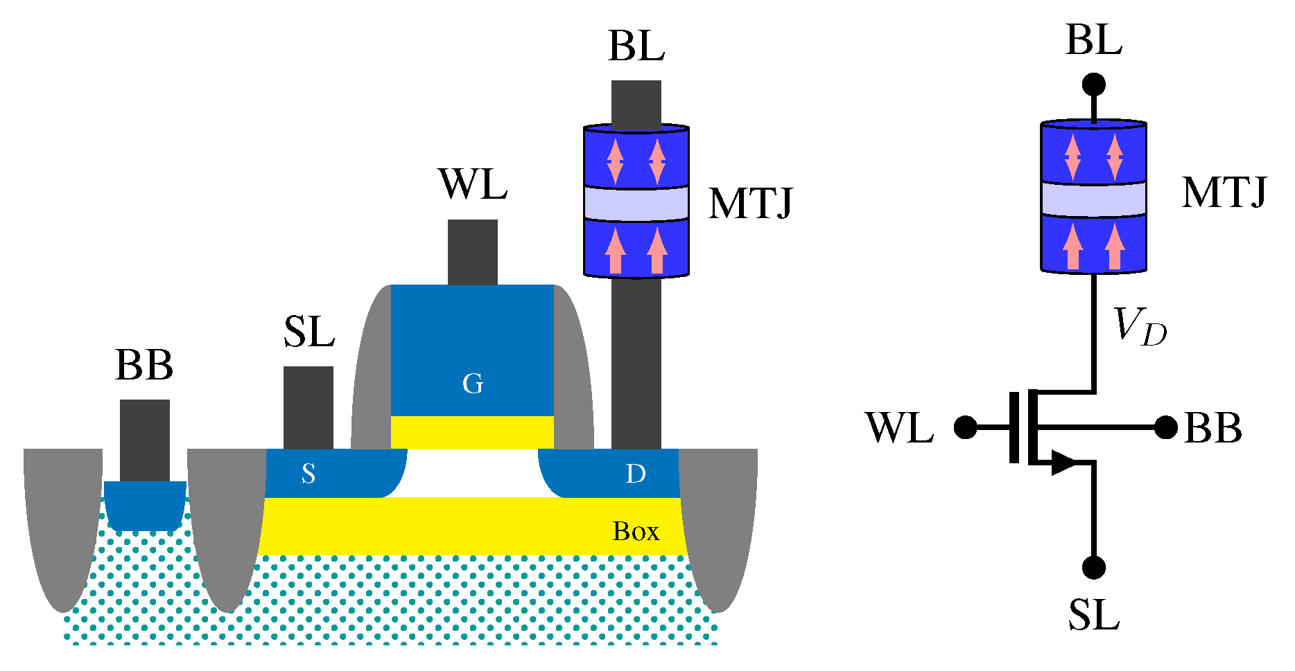
2. VCMA-MTJ
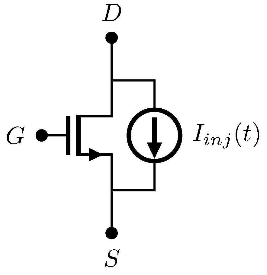
3. SET Model
4. Simulations and Results
4.1. VCMA-MTJ Based MeRAM Bit-Cell
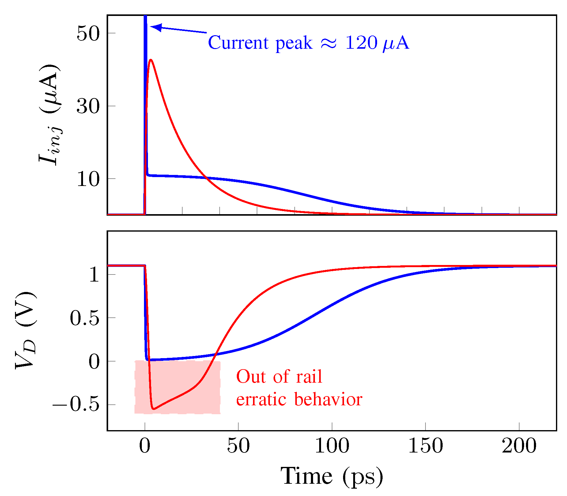
4.2. SET Analysis
4.2.1. Case 1: Without Write Pulse
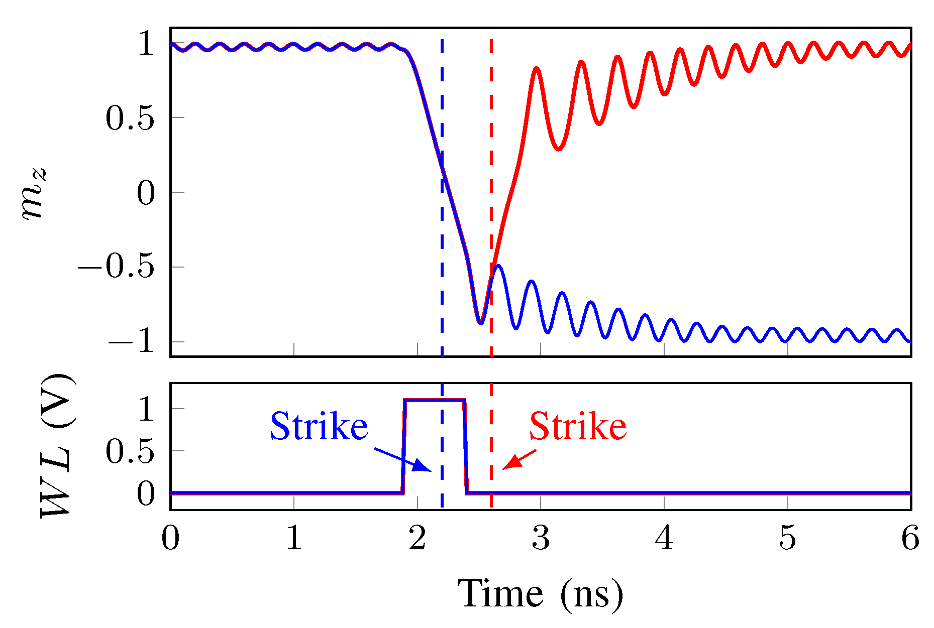
4.2.2. Case 2: With Write Pulse
4.2.3. Case 3: Modulation of the Transistor Channel Width (W)
5. Conclusions
Author Contributions
Funding
Conflicts of Interest
Abbreviations
| AP | Anti-Parallel |
| BL | Bit-Line |
| CMOS | Complementary Metal Oxide Semiconductor |
| FDSOI | Fully Depleted Silicon-on-Insulator |
| LET | Linear Energy Transfer |
| LVT | Low Threshold Voltage |
| MeRAM | Magnetoelectric Random Access Memory |
| MOS | Metal Oxide Semiconductor |
| MRAM | Magnetic Random Access Memory |
| MTJ | Magnetic Tunnel Junction |
| NVM | Non-Volatile Memory |
| P | Parallel |
| PMA | Perpendicular Magnetic Anisotropy |
| SET | Single-Event Transient |
| STT | Spin Transfer Torque |
| TCAD | Technology computer-aided design |
| TMR | Tunnel Magnetoresistance |
| VCMA | Voltage-Controlled Magnetic Anisotropy |
| WL | Word-Line |
References
- Chappert, C.; Fert, A.; Dau, F.N.V. The emergence of spin electronics in data storage. Nat. Mater. 2007, 6, 813–823. [Google Scholar] [CrossRef] [PubMed]
- Kang, W.; Chang, L.; Zhang, Y.; Zhao, W. Voltage-controlled MRAM for working memory: Perspectives and challenges. In Proceedings of the Design, Automation Test in Europe Conference Exhibition (DATE), Lausanne, Switzerland, 27–31 March 2017; pp. 542–547. [Google Scholar]
- Maruyama, T.; Shiota, Y.; Nozaki, T.; Ohta, K.; Toda, N.; Mizuguchi, M.; Tulapurkar, A.A.; Shinjo, T.; Shiraishi, M.; Mizukami, S.; et al. Large voltage-induced magnetic anisotropy change in a few atomic layers of iron. Nat. Nanotechnol. 2009, 4, 158–161. [Google Scholar] [CrossRef] [PubMed]
- Shiota, Y.; Nozaki, T.; Bonell, F.; Murakami, S.; Shinjo, T.; Suzuki, Y. Induction of coherent magnetization switching in a few atomic layers of FeCo using voltage pulses. Nat. Mater. 2012, 11, 39–43. [Google Scholar] [CrossRef] [PubMed]
- Sharmin, S.; Jaiswal, A.; Roy, K. Modeling and design space exploration for bit-cells based on voltage-assisted switching of magnetic tunnel junctions. IEEE Trans. Electron Devices 2016, 63, 3493–3500. [Google Scholar] [CrossRef]
- Kang, W.; Ran, Y.; Zhang, Y.; Lv, W.; Zhao, W. Modeling and exploration of the voltage-controlled magnetic anisotropy effect for the next-generation low-power and high-speed MRAM applications. IEEE Trans. Nanotechnol. 2017, 16, 387–395. [Google Scholar] [CrossRef]
- Wang, S.; Lee, H.; Ebrahimi, F.; Amiri, P.K.; Wang, K.L.; Gupta, P. Comparative Evaluation of Spin-Transfer-Torque and Magnetoelectric Random Access Memory. IEEE J. Emerg. Sel. Top. Circuits Syst. 2016, 6, 134–145. [Google Scholar] [CrossRef]
- Yang, J.; Wang, P.; Zhang, Y.; Cheng, Y.; Zhao, W.; Chen, Y.; Li, H.H. Radiation-Induced Soft Error Analysis of STT-MRAM: A Device to Circuit Approach. IEEE Trans. Comput.-Aided Des. Integr. Circuits Syst. 2016, 35, 380–393. [Google Scholar] [CrossRef]
- Cai, H.; Wang, Y.; Kang, W.; Naviner, L.; Shan, W.; Yang, J.; Zhao, W. Enabling Resilient Voltage-Controlled MeRAM Using Write Assist Techniques. In Proceedings of the 2018 IEEE International Symposium on Circuits and Systems (ISCAS), Florence, Italy, 27–30 May 2018; pp. 1–5. [Google Scholar] [CrossRef]
- International Technology Roadmap for Semiconductors: Design. ITRS 2009 Edition. Available online: http://www.itrs2.net/itrs-reports.html (accessed on 15 December 2018).
- Pilia, R.; Bascoul, G.; Sanchez, K.; Mura, G.; Infante, F. Single Event Transient acquisition and mapping for space device Characterization. Microelectron. Reliab. 2016, 64, 73–78. [Google Scholar] [CrossRef]
- Kang, W.; Zhao, W.; Deng, E.; Klein, J.O.; Cheng, Y.; Ravelosona, D.; Zhang, Y.; Chappert, C. A radiation hardened hybrid spintronic/CMOS nonvolatile unit using magnetic tunnel junctions. J. Phys. D Appl. Phys. 2014, 47, 405003. [Google Scholar] [CrossRef]
- Bartra, W.C.; Vladimirescu, A.; Reis, R. FDSOI and Bulk CMOS SRAM Cell Resilience to Radiation Effects. Microelectron. Reliab. 2016, 64, 152–157. [Google Scholar] [CrossRef]
- Liu, R. Study of Radiation Effects on 28 nm UTBB FDSOI Technology. Ph.D. Dissertation, University of Saskatchewan, Saskatoon, SK, Canada, 2017. [Google Scholar]
- Bartra, W.C.; Vladimirescu, A.; Reis, R. Process and temperature impact on single-event transients in 28 nm FDSOI CMOS. In Proceedings of the 2017 IEEE 8th Latin American Symposium on Circuits Systems (LASCAS), Bariloche, Argentina, 30–23 February 2017; pp. 1–4. [Google Scholar] [CrossRef]
- Cai, H.; Wang, Y.; de Barros Naviner, L.A.; Liu, X.; Shan, W.; Yang, J.; Zhao, W. Addressing Failure and Aging Degradation in MRAM/MeRAM-on-FDSOI Integration. IEEE Trans. Circuits Syst. I Regul. Pap. 2018, 1–12. [Google Scholar] [CrossRef]
- Maciel, N.; Marques, E.C.; Naviner, L.A.B.; Cai, H. Single-Event Transient Effects on Dynamic Comparator in 28 nm FDSOI CMOS Technology. Microelectron. Reliab. 2018, 88, 965–968. [Google Scholar] [CrossRef]
- Zhang, D.; Zeng, L.; Zhang, Y.; Klein, J.O.; Zhao, W. Reliability-Enhanced Hybrid CMOS/MTJ Logic Circuit Architecture. IEEE Trans. Magn. 2017, 53, 1–5. [Google Scholar] [CrossRef]
- Deng, E.; Kang, W.; Zhang, Y.; Klein, J.; Chappert, C.; Zhao, W. Design Optimization and Analysis of Multicontext STT-MTJ/CMOS Logic Circuits. IEEE Trans. Nanotechnol. 2015, 14, 169–177. [Google Scholar] [CrossRef]
- Kang, W.; Deng, E.; Klein, J.; Zhang, Y.; Zhang, Y.; Chappert, C.; Ravelosona, D.; Zhao, W. Separated Precharge Sensing Amplifier for Deep Submicrometer MTJ/CMOS Hybrid Logic Circuits. IEEE Trans. Magn. 2014, 50, 1–5. [Google Scholar] [CrossRef]
- Cai, H.; Wang, Y.; de Barros Naviner, L.A.; Yang, J.; Zhao, W. Exploring Hybrid STT-MTJ/CMOS Energy Solution in Near-/Sub-Threshold Regime for IoT Applications. IEEE Trans. Magn. 2018, 54, 1–9. [Google Scholar] [CrossRef]
- Berger, L. Emission of spin waves by a magnetic multilayer traversed by a current. Phys. Rev. B 1996, 54, 9353–9358. [Google Scholar] [CrossRef]
- Wang, W.; Li, M.; Hageman, S.; Chien, C. Electric-field-assisted switching in magnetic tunnel junctions. Nat. Mater. 2012, 11, 64–68. [Google Scholar] [CrossRef] [PubMed]
- Barnes, S.E.; Ieda, J.I.; Maekawa, S. Rashba spin–orbit anisotropy and the electric field control of magnetism. Sci. Rep. 2014, 4, 1–5. [Google Scholar] [CrossRef]
- Velev, J.P.; Jaswal, S.S.; Tsymbal, E.Y. Multi-ferroic and magnetoelectric materials and interfaces. Philos. Trans. R. Soc. A Math. Phys. Eng. Sci. 2011, 369, 3069–3097. [Google Scholar] [CrossRef] [Green Version]
- Messenger, G.C. Collection of Charge on Junction Nodes from Ion Tracks. IEEE Trans. Nucl. Sci. 1982, 29, 2024–2031. [Google Scholar] [CrossRef]
- Singh, M.; Koren, I. Fault-sensitivity analysis and reliability enhancement of analog-to-digital converters. IEEE Trans. Very Large Scale Integr. Syst. 2003, 11, 839–852. [Google Scholar] [CrossRef] [Green Version]
- Malherbe, V.; Gasiot, G.; Soussan, D.; Autran, J.; Roche, P. On-Orbit Upset Rate Prediction at Advanced Technology Nodes: A 28 nm FD-SOI Case Study. IEEE Trans. Nucl. Sci. 2017, 64, 449–456. [Google Scholar] [CrossRef]
- Malherbe, V.; Gasiot, G.; Soussan, D.; Patris, A.; Autran, J.; Roche, P. Alpha soft error rate of FDSOI 28 nm SRAMs: Experimental testing and simulation analysis. In Proceedings of the 2015 IEEE International Reliability Physics Symposium, Monterey, CA, USA, 19–23 April 2015; pp. SE.11.1–SE.11.6. [Google Scholar] [CrossRef]
- Kauppila, J.S.; Sternberg, A.L.; Alles, M.L.; Francis, A.M.; Holmes, J.; Amusan, O.A.; Massengill, L.W. A Bias-Dependent Single-Event Compact Model Implemented Into BSIM4 and a 90 nm CMOS Process Design Kit. IEEE Trans. Nucl. Sci. 2009, 56, 3152–3157. [Google Scholar] [CrossRef]
- Kobayashi, D.; Makino, T.; Hirose, K. Analytical Expression for Temporal Width Characterization of Radiation-induced Pulse Noises in SOI CMOS Logic Gates. In Proceedings of the IEEE International Physics Reliability Symposium, Montreal, QC, Canada, 26–30 April 2009; pp. 165–169. [Google Scholar]
- Fulkerson, D.E.; Vogt, E.E. Prediction of SOI Single Event Effects Using a Simple Physics Based SPICE Model. IEEE Trans. Nucl. Sci. 2005, 51, 2168–2174. [Google Scholar] [CrossRef]
- Black, D.A.; Robinson, W.H.; Wilcox, I.Z.; Limbrick, D.B.; Black, J.D. Modeling of Single Event Transients with Dual Double-Exponential Current Sources: Implications for Logic Cell Characterization. IEEE Trans. Nucl. Sci. 2015, 62, 1540–1549. [Google Scholar] [CrossRef]
- Clark, K.A.; Ross, A.A.; Loomis, H.H.; Weatherford, T.R.; Fouts, D.J.; Buchner, S.P.; McMorrow, D. Modeling single-event effects in a complex digital device. IEEE Trans. Nucl. Sci. 2003, 50, 2069–2080. [Google Scholar] [CrossRef] [Green Version]
- Fong, X.; Kim, Y.; Choday, S.H.; Roy, K. Failure mitigation techniques for 1T-1MTJ spin-transfer torque MRAM bit-cells. IEEE Trans. Very Large Scale Integr. Syst. 2014, 22, 384–395. [Google Scholar] [CrossRef]
- Wang, Y.; Cai, H.; Naviner, L.; Zhao, X.; Zhang, Y.; Slimani, M.; Klein, J.; Zhao, W. A process-variation-resilient methodology of circuit design by using asymmetrical forward body bias in 28 nm FDSOI. Microelectron. Reliab. 2016, 64, 26–30. [Google Scholar] [CrossRef]
- Long, M.; Zeng, L.; Gao, T.; Zhang, D.; Qin, X.; Zhang, Y.; Zhao, W. Self-Adaptive Write Circuit for Magnetic Tunneling Junction Memory with Voltage-Controlled Magnetic Anisotropy Effect. IEEE Trans. Nanotechnol. 2018, 17, 492–499. [Google Scholar] [CrossRef]
- Lee, H.; Lee, A.; Wang, S.; Ebrahimi, F.; Gupta, P.; Amiri, P.K.; Wang, K.L. A Word Line Pulse Circuit Technique for Reliable Magnetoelectric Random Access Memory. IEEE Trans. Very Large Scale Integr. Syst. 2017, 25, 2027–2034. [Google Scholar] [CrossRef]


| Parameter | Description | Value |
|---|---|---|
| T | Temperature | 300 K |
| TMR(0) | TMR ratio at | |
| , | MTJ resistance | 100 k, 200 k |
| Thermal stability at | 40 | |
| TMR Bias voltage | V | |
| MgO oxide thickness | nm | |
| Free layer thickness | nm | |
| d | MTJ diameter | 50 nm |
| Damping factor | ||
| Interfacial PMA | J/m | |
| Saturation magnetization | A/m | |
| VCMA coefficient | 60 fJ/V·m | |
| External magnetic field | 400 Oe |
© 2019 by the authors. Licensee MDPI, Basel, Switzerland. This article is an open access article distributed under the terms and conditions of the Creative Commons Attribution (CC BY) license (http://creativecommons.org/licenses/by/4.0/).
Share and Cite
Maciel, N.; Marques, E.C.; Naviner, L.; Cai, H.; Yang, J. Voltage-Controlled Magnetic Anisotropy MeRAM Bit-Cell over Event Transient Effects. J. Low Power Electron. Appl. 2019, 9, 15. https://doi.org/10.3390/jlpea9020015
Maciel N, Marques EC, Naviner L, Cai H, Yang J. Voltage-Controlled Magnetic Anisotropy MeRAM Bit-Cell over Event Transient Effects. Journal of Low Power Electronics and Applications. 2019; 9(2):15. https://doi.org/10.3390/jlpea9020015
Chicago/Turabian StyleMaciel, Nilson, Elaine C. Marques, Lirida Naviner, Hao Cai, and Jun Yang. 2019. "Voltage-Controlled Magnetic Anisotropy MeRAM Bit-Cell over Event Transient Effects" Journal of Low Power Electronics and Applications 9, no. 2: 15. https://doi.org/10.3390/jlpea9020015