Flyback Converter for Solid-State Lighting Applications with Partial Energy Processing

 ,
, 
 ,
, 
 ,
,  ,
,  ,
,  and
and 
Abstract
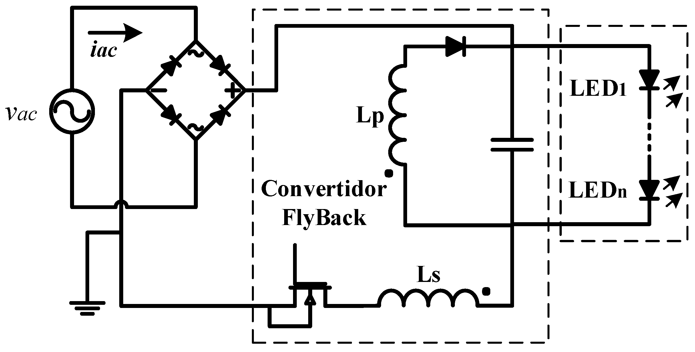
1. Introduction
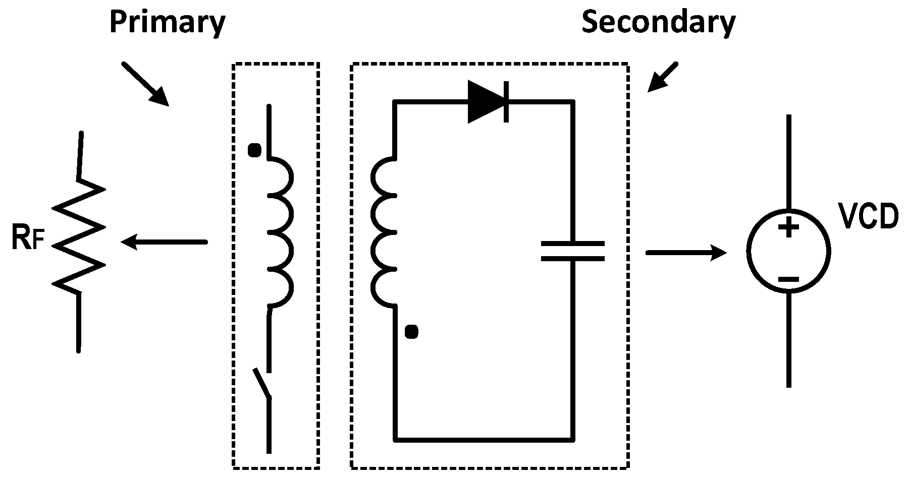
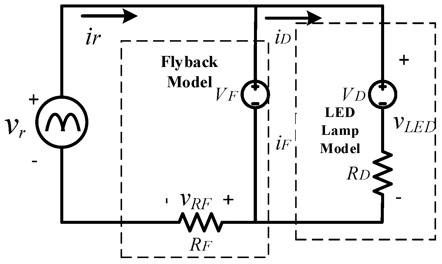
2. Mathematical Analysis of the Proposed Circuit
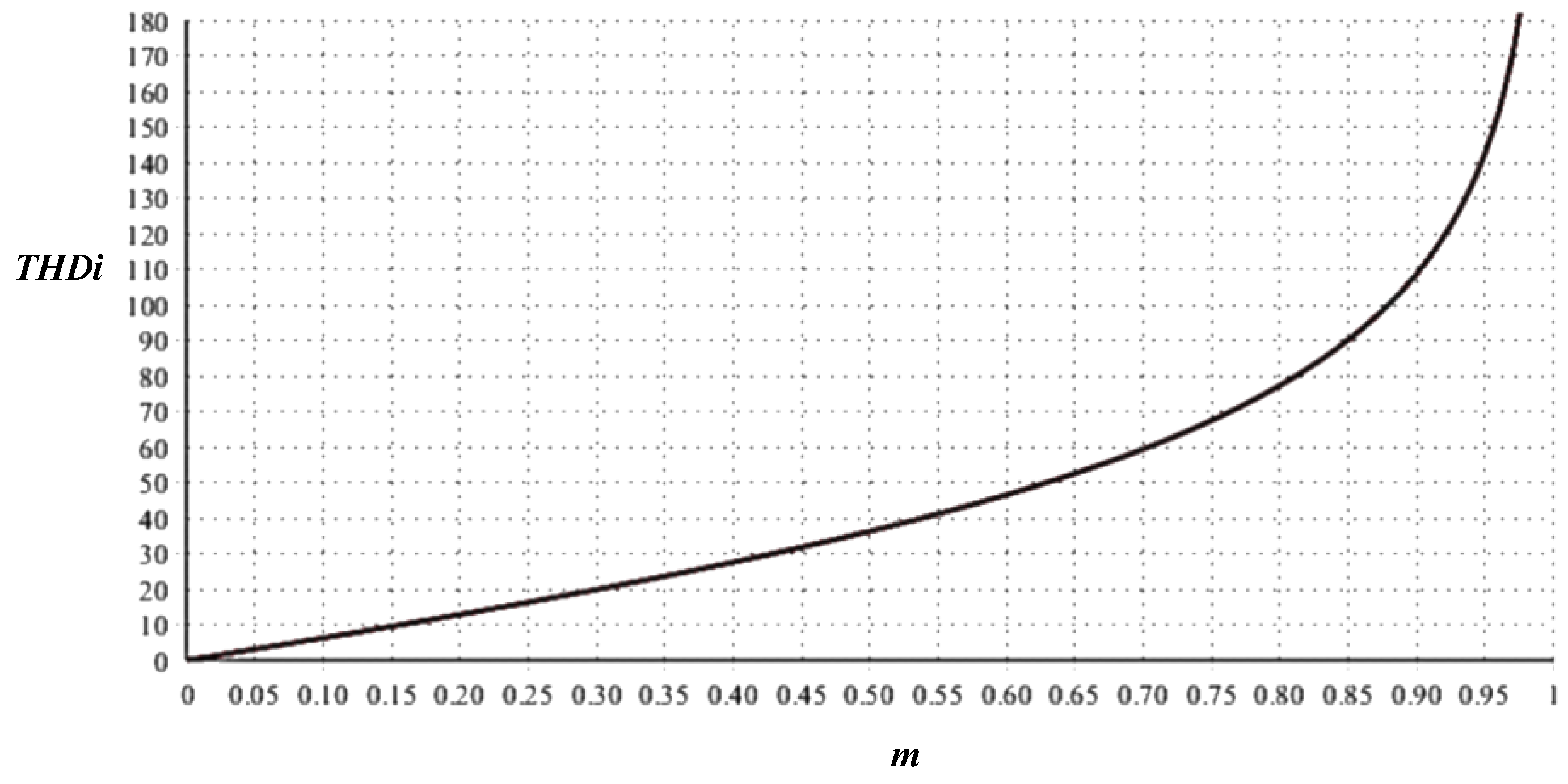
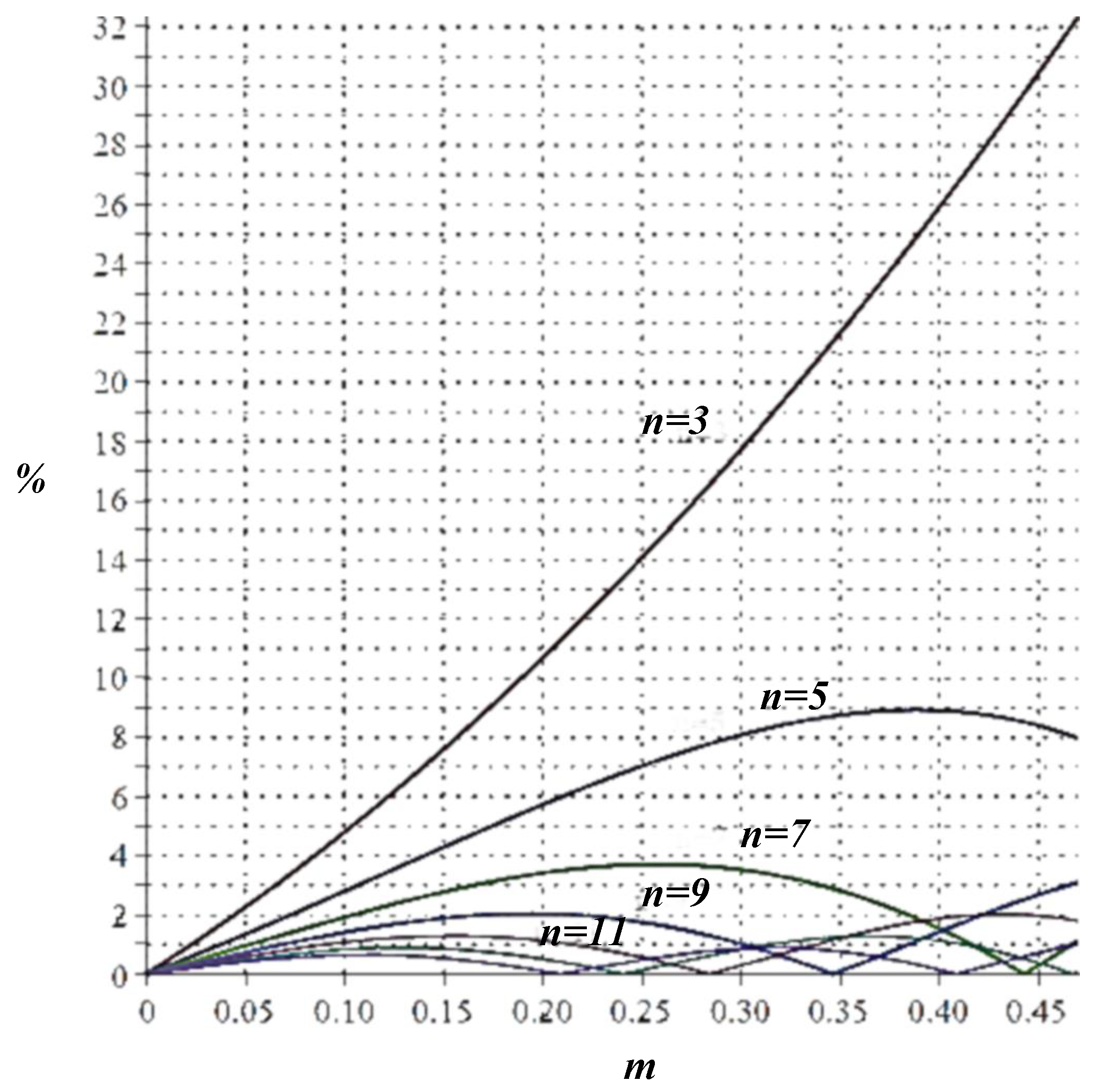
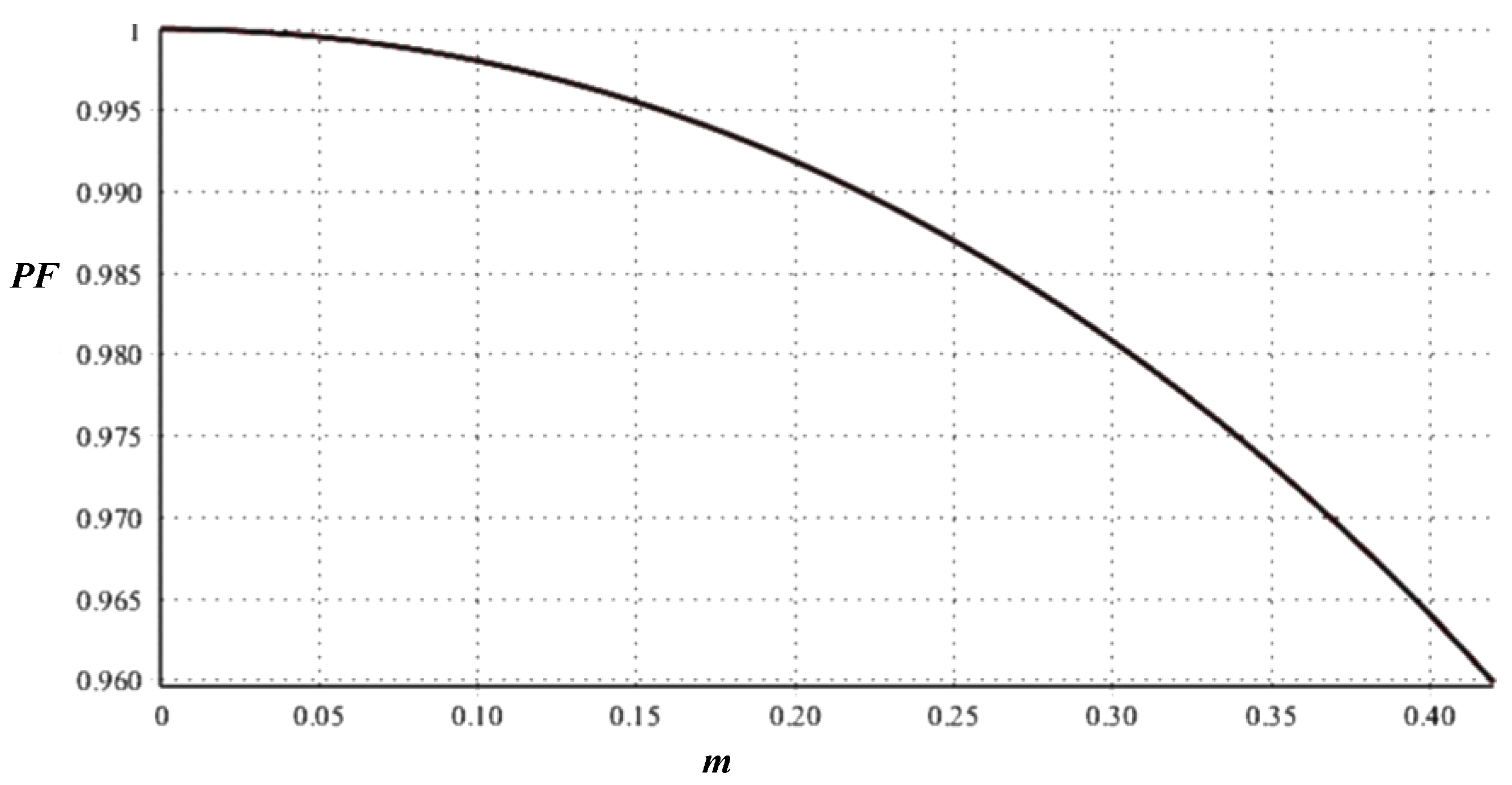
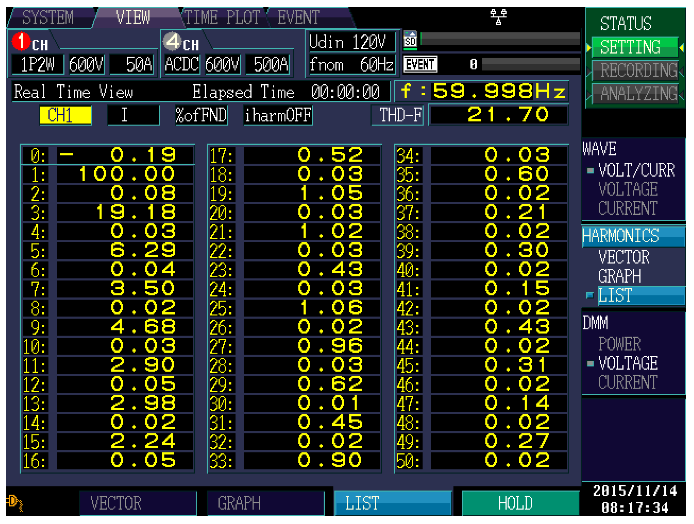
2.1. Analysis of the Power Factor (PF) and the Current Total Harmonic Distortion (THDi) Using LAAA
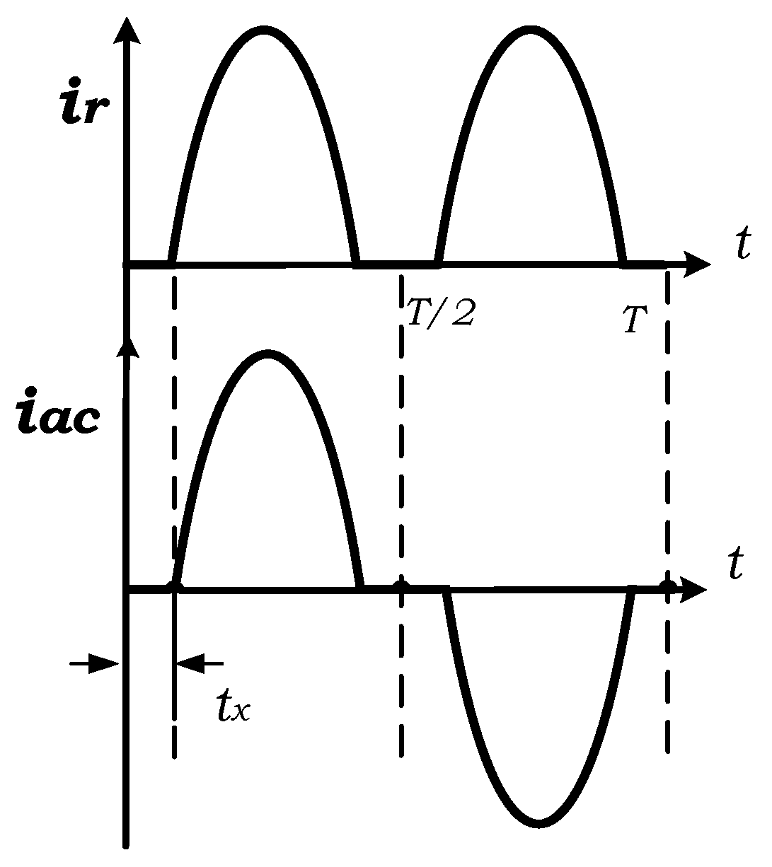
- The topology is reductive, so it is always true that VF < Vr, where Vr is the peak voltage of vr(t), as shown in (4).
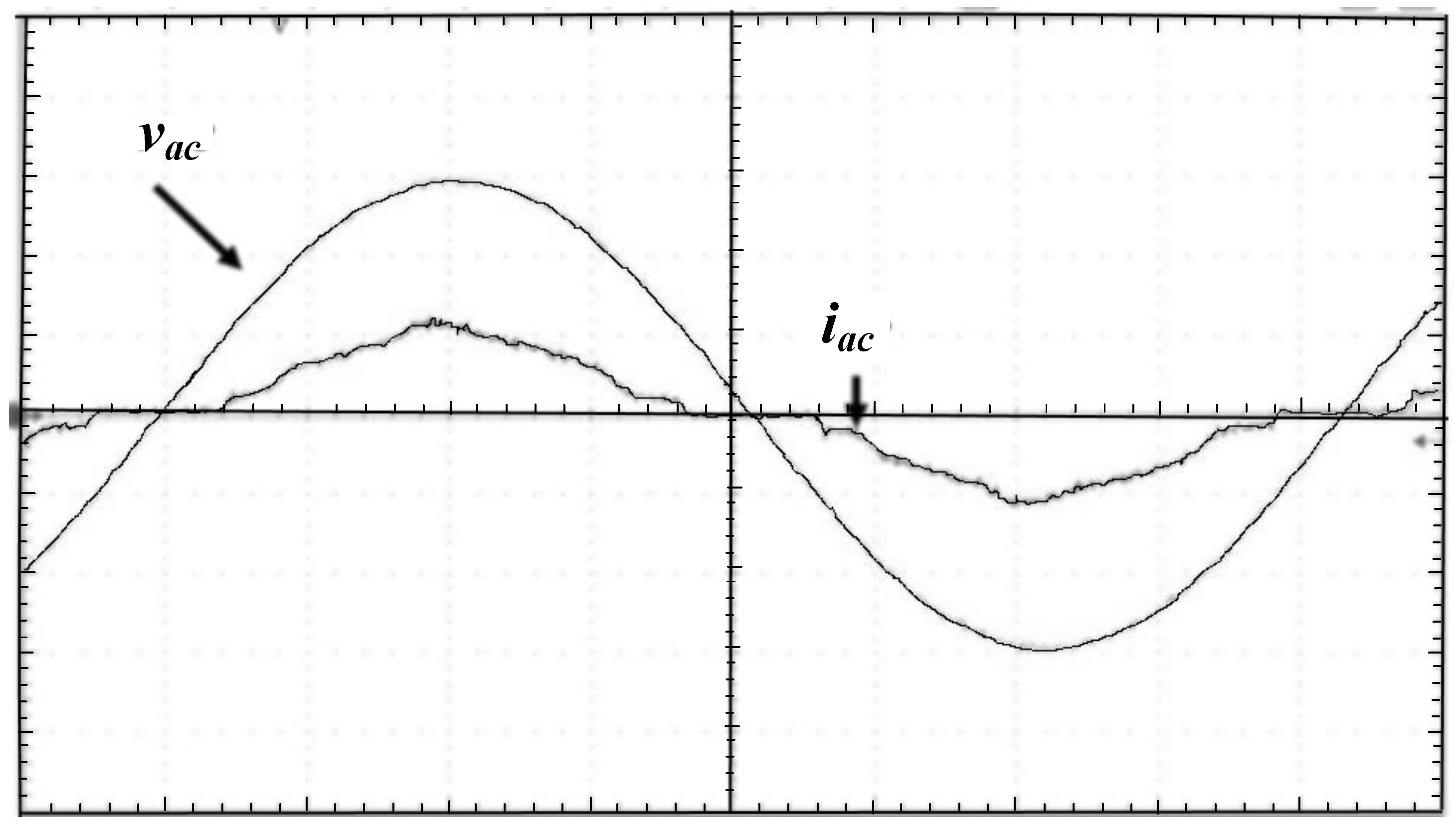
- There will be current flow through RF if vr > VF, when vr < VF the current ir(t) = 0, as Vr approaches VF there will be very long death times. Therefore, the ir waveform will be the same as iac at T/2 as shown in Figure 5.
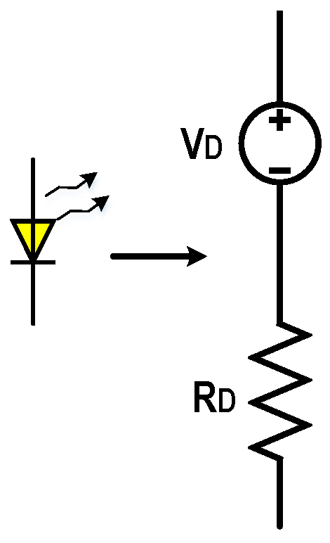
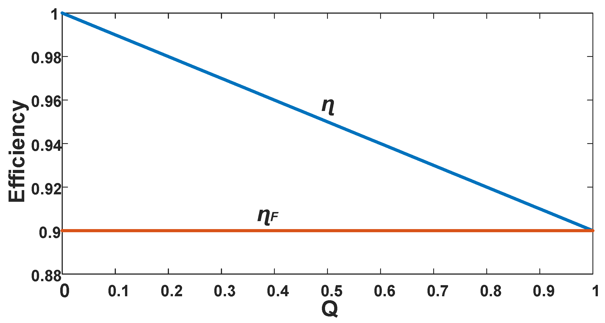
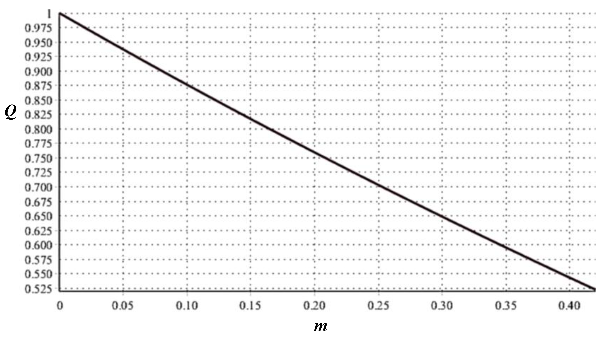
2.2. Analysis of the Power Flow in the Converter
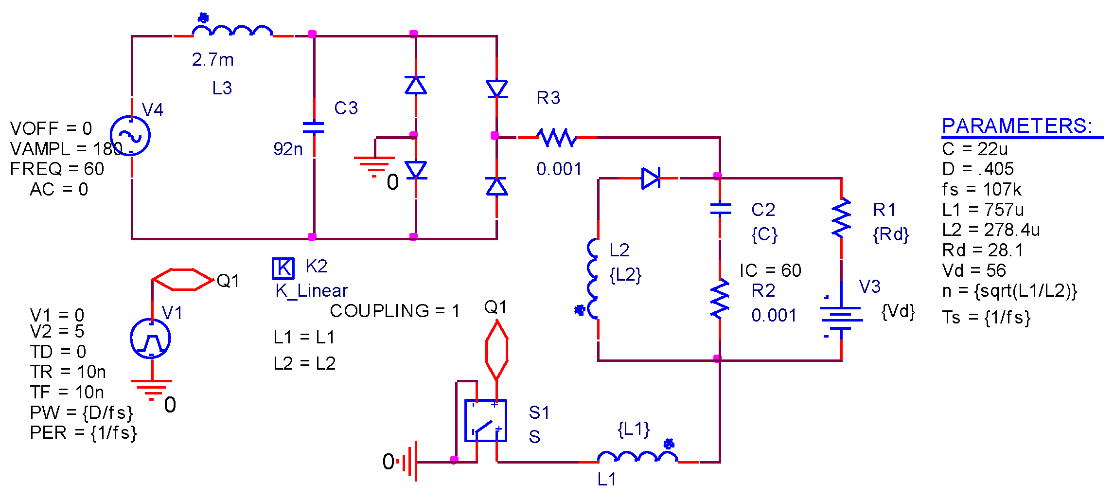
3. Design of the Rearranged Flyback
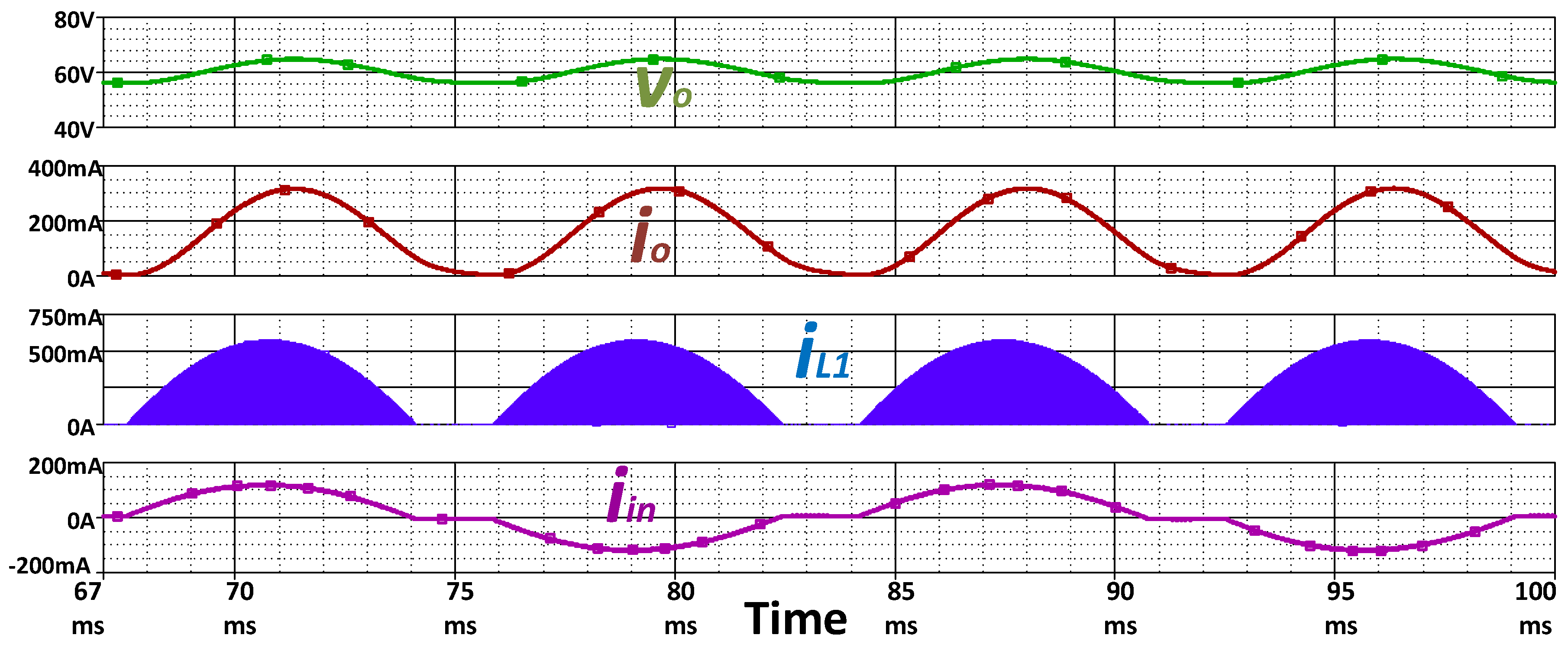
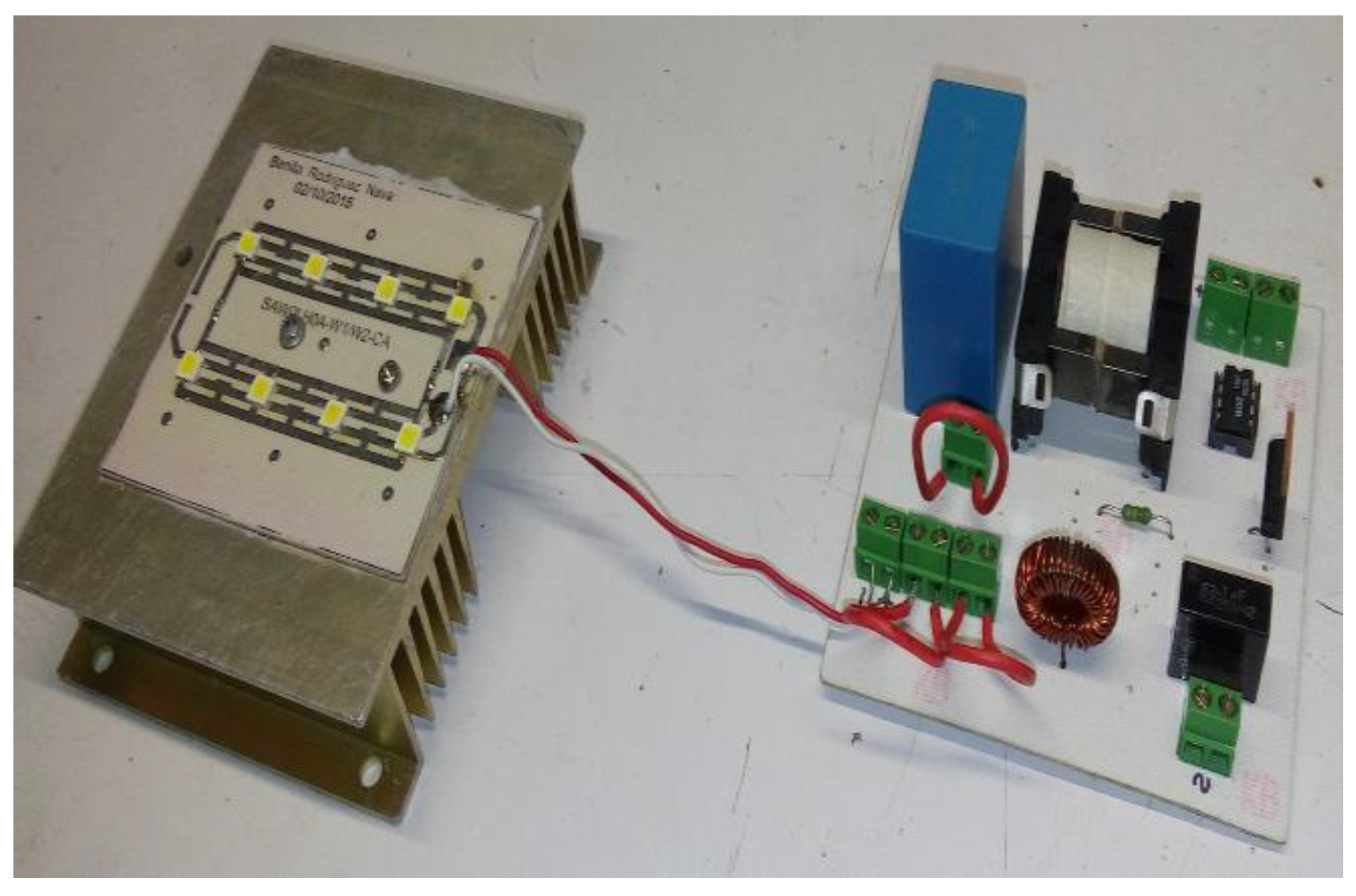
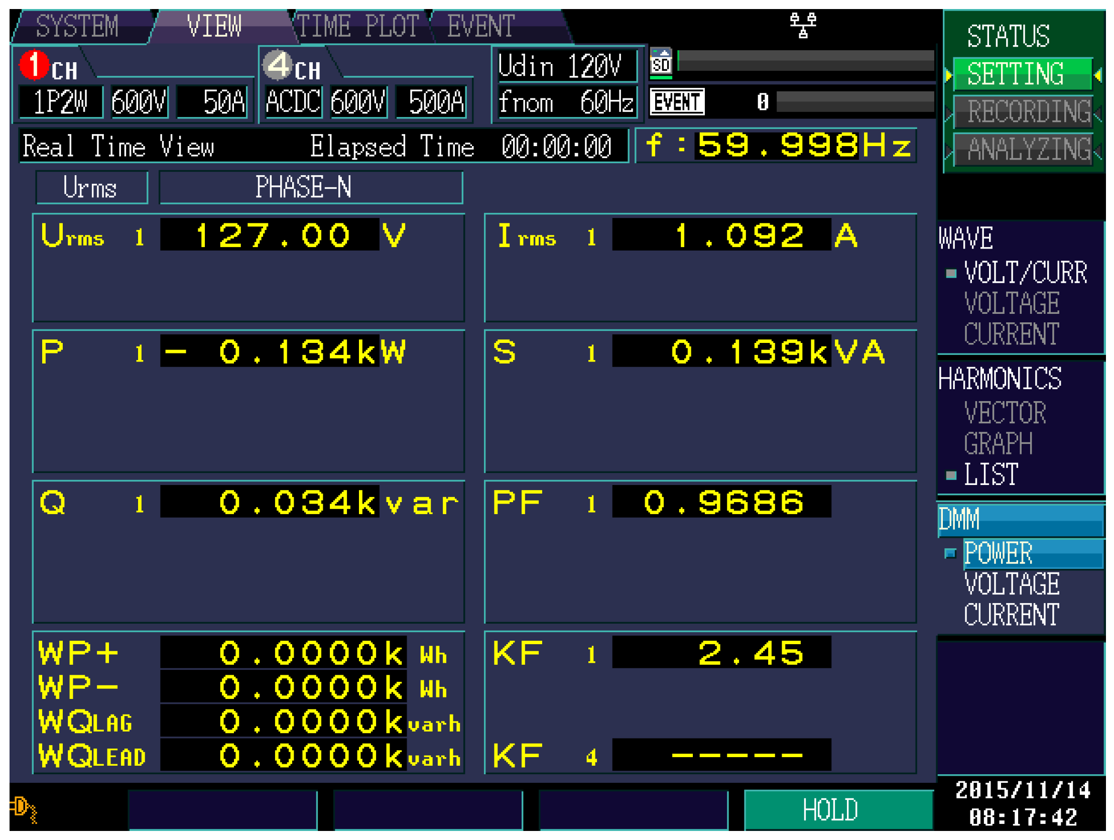
4. Experimental Results
5. Conclusions
Author Contributions
Funding
Conflicts of Interest
References
- Energy Efficiency and Renewable Energy Information Center. Lifetime of White LEDs; U.S. Department of Energy: Washington, DC, USA, 2009. Available online: http://apps1.eere.energy.gov/buildings/publications/pdfs/ssl/lifetime_white_leds.pdf (accessed on 17 February 2017).
- ENERGY STAR®Program Requirements for Solid State Lighting Luminaires. Available online: https://www.energystar.gov/ia/partners/product_specs/program_reqs/SSL_prog_req_V1.1.pdf (accessed on 20 March 2017).
- Electromagnetic compatibility, Part 3, Section 2. In Limits for Harmonic Current Emissions (Equipment Input Current ≤ 16A Per Phase); IEC 61000-3-2; IEC: Geneva, Switzerland, 2005.
- Wang, S.; Ruan, X.; Yao, K.; Ye, Z. A flicker-free electrolytic capacitor-less ac-dc LED driver. In Proceedings of the 2011 IEEE Energy Conversion Congress and Exposition, Phoenix, AZ, USA, 17–22 September 2011; pp. 2318–2325. [Google Scholar]
- Ponce, M.; Martinez, A.J.; Correa, J.; Arau, J.; Alonso, J.M. An efficient integrated electronic ballast for compact fluorescent lamps. In Proceedings of the Power Electronics Specialists Conference, Cairns, Australia, 23–27 June 2002; Volume 201, pp. 203–208. [Google Scholar]
- Qiu, Y.; Wang, L.; Wang, H.; Liu, Y.F.; Sen, P.C. Bipolar Ripple Cancellation Method to Achieve Single-Stage Electrolytic-Capacitor-Less High-Power LED Driver. IEEE J. Emerg. Sel. Top. Power Electron. 2015, 3, 698–713. [Google Scholar] [CrossRef]
- Han, L.; Narendran, N. An Accelerated Test Method for Predicting the Useful Life of an LED Driver. IEEE Trans. Power Electron. 2011, 26, 2249–2257. [Google Scholar] [CrossRef]
- Buiatti, G.M.; Cruz, S.M.A.; Cardoso, A.J.M. Lifetime of Film Capacitors in Single-Phase Regenerative Induction Motor Drives. In Proceedings of the 2007 IEEE International Symposium on Diagnostics for Electric Machines, Power Electronics and Drives, Atlanta, GA, USA, 6–8 September 2007; pp. 356–362. [Google Scholar]
- Chiu, H.J.; Huang, H.M.; Yang, H.T.; Cheng, S.J. An improved single-stage Flyback PFC converter for high-luminance lighting LED lamps. Int. J. Circuit Theory Appl. 2008, 36, 205–210. [Google Scholar] [CrossRef]
- Chiu, H.J.; Cheng, S.J. Design considerations of an SEPIC PFC converter for driving multiple lighting LED lamps. Int. J. Circuit Theory Appl. 2009, 37, 928–940. [Google Scholar] [CrossRef]
- Delgado-Antillón, C.P.; Morales-Saldaña, J.A.; Peña-Gallardo, R.; Moreno-Basaldua, E.; Loera-Palomo, R. Optimized design of a quadratic boost converter based on the R2P2 principle. In Proceedings of the 2016 IEEE International Autumn Meeting on Power, Electronics and Computing (ROPEC), Ixtapa, Mexico, 9–11 November 2016; pp. 1–6. [Google Scholar]
- Lam, J.C.W.; Jain, P.K. Isolated AC/DC Offline High Power Factor Single-Switch LED Drivers Without Electrolytic Capacitors. IEEE J. Emerg. Sel. Top. Power Electron. 2015, 3, 679–690. [Google Scholar] [CrossRef]
- Lam, J.C.W.; Jain, P.K. A High Power Factor, Electrolytic Capacitor-Less AC-Input LED Driver Topology With High Frequency Pulsating Output Current. IEEE Trans. Power Electron. 2015, 30, 943–955. [Google Scholar] [CrossRef]
- Arias, M.; Lamar, D.G.; Sebastian, J.; Balocco, D.; Diallo, A.A. High-Efficiency LED Driver Without Electrolytic Capacitor for Street Lighting. IEEE Trans. Ind. Appl. 2013, 49, 127–137. [Google Scholar] [CrossRef]
- Yang, J.; Faris, A.N.; Zhang, W.; Liu, Y.; Chen, X. A universal-input high-power-factor LLC resonant driver without electrolytic capacitor for PWM dimming LED lighting application. In Proceedings of the 2014 International Power Electronics and Application Conference and Exposition, Shanghai, China, 5–8 November 2014; pp. 1473–1478. [Google Scholar]
- Qi, W.; Li, S.; Yuan, H.; Tan, S.; Hui, S. High-Power-Density Single-Phase Three-Level Flying-Capacitor Buck PFC Rectifier. IEEE Trans. Power Electron. 2019, 34, 10833–10844. [Google Scholar] [CrossRef]
- Chen, W.; Hui, S.Y.R. Elimination of an Electrolytic Capacitor in AC/DC Light-Emitting Diode (LED) Driver With High Input Power Factor and Constant Output Current. IEEE Trans. Power Electron. 2012, 27, 1598–1607. [Google Scholar] [CrossRef]
- Morales-Saldaña, J.A.; Loera-Palomo, R.; Palacios-Hernández, E.; González-Martínez, J.L. Modelling and control of a DC-DC quadratic boost converter with R2P2. IET Power Electron. 2014, 7, 11–22. [Google Scholar] [CrossRef]
- Leung, K.H.; Wong, C.S.; Loo, K.H.; Lai, Y.M.; Chow, M.H.L. Elimination of electrolytic capacitor through high-voltage driving of LED aided by third-order harmonic current injection. In Proceedings of the IECON 2013—39th Annual Conference of the IEEE Industrial Electronics Society, Vienna, Austria, 10–13 November 2013; pp. 6058–6062. [Google Scholar]
- Wang, B.; Ruan, X.; Yao, K.; Xu, M. A Method of Reducing the Peak-to-Average Ratio of LED Current for Electrolytic Capacitor-Less AC-DC Drivers. IEEE Trans. Power Electron. 2010, 25, 592–601. [Google Scholar] [CrossRef]
- Ruan, X.; Wang, B.; Yao, K.; Wang, S. Optimum Injected Current Harmonics to Minimize Peak-to-Average Ratio of LED Current for Electrolytic Capacitor-Less AC–DC Drivers. IEEE Trans. Power Electron. 2011, 26, 1820–1825. [Google Scholar] [CrossRef]
- Camponogara, D.; Ferreira, G.F.; Campos, A.; Costa, M.A.D.; Garcia, J. Offline LED Driver for Street Lighting With an Optimized Cascade Structure. IEEE Trans. Ind. Appl. 2013, 49, 2437–2443. [Google Scholar] [CrossRef]
- Lee, K.W.; Hsieh, Y.H.; Liang, T.J. A current ripple cancellation circuit for electrolytic capacitor-less AC-DC LED driver. In Proceedings of the 2013 Twenty-Eighth Annual IEEE Applied Power Electronics Conference and Exposition (APEC), Long Beach, CA, USA, 17–21 March 2013; pp. 1058–1061. [Google Scholar]
- Wang, S.; Ruan, X.; Yao, K.; Tan, S.C.; Yang, Y.; Ye, Z. A Flicker-Free Electrolytic Capacitor-Less AC–DC LED Driver. IEEE Trans. Power Electron. 2012, 27, 4540–4548. [Google Scholar] [CrossRef]
- Wang, L.; Zhang, B.; Qiu, D.; Wang, L. A novel flicker-free AC-DC LED driver without electrolytic capacitor. In Proceedings of the 2017 IEEE International Conference on Industrial Technology (ICIT), Toronto, ON, Canada, 22–25 March 2017; pp. 370–375. [Google Scholar]
- He, J.; Ruan, X.; Zhang, L. Adaptive Voltage Control for Bidirectional Converter in Flicker-Free Electrolytic Capacitor-Less AC–DC LED Driver. IEEE Trans. Ind. Electron. 2017, 64, 320–324. [Google Scholar] [CrossRef]
- Zhang, L.; Ruan, X.; Ren, X. One-Cycle Control for Electrolytic Capacitor-Less Second Harmonic Current Compensator. IEEE Trans. Power Electron. 2018, 33, 1724–1739. [Google Scholar] [CrossRef]
- Yang, Y.; Ruan, X.; Zhang, L.; He, J.; Ye, Z. Feed-Forward Scheme for an Electrolytic Capacitor-Less AC/DC LED Driver to Reduce Output Current Ripple. IEEE Trans. Power Electron. 2014, 29, 5508–5517. [Google Scholar] [CrossRef]
- Ni, Y.; Pervaiz, S.; Chen, M.; Afridi, K.K. Energy Density Enhancement of Stacked Switched Capacitor Energy Buffers Through Capacitance Ratio Optimization. IEEE Trans. Power Electron. 2017, 32, 6363–6380. [Google Scholar] [CrossRef]
- Chen, M.; Ni, Y.; Serrano, C.; Montgomery, B.; Perreault, D.; Afridi, K. An electrolytic-free offline LED driver with a ceramic-capacitor-based compact SSC energy buffer. In Proceedings of the 2014 IEEE Energy Conversion Congress and Exposition (ECCE), Pittsburgh, PA, USA, 14–18 September 2014; pp. 2713–2718. [Google Scholar]
- Gu, L.; Ruan, X.; Xu, M.; Yao, K. Means of Eliminating Electrolytic Capacitor in AC/DC Power Supplies for LED Lightings. IEEE Trans. Power Electron. 2009, 24, 1399–1408. [Google Scholar] [CrossRef]
- Tang, Y.; Blaabjerg, F. Power decoupling techniques for single-phase power electronics systems—An overview. In Proceedings of the 2015 IEEE Energy Conversion Congress and Exposition (ECCE), Montreal, QC, Canada, 20–24 September 2015; pp. 2541–2548. [Google Scholar]
- Qin, Z.; Tang, Y.; Loh, P.C.; Blaabjerg, F. Benchmark of AC and DC Active Power Decoupling Circuits for Second-Order Harmonic Mitigation in Kilowatt-Scale Single-Phase Inverters. IEEE J. Emerg. Sel. Top. Power Electron. 2016, 4, 15–25. [Google Scholar] [CrossRef]
- Zhang, L.; Ruan, X. Control Schemes for Reducing Second Harmonic Current in Two-Stage Single-Phase Converter: An Overview From DC-Bus Port-Impedance Characteristics. IEEE Trans. Power Electron. 2019, 34, 10341–10358. [Google Scholar] [CrossRef]
- Tang, Y.; Blaabjerg, F.; Loh, P.C.; Jin, C.; Wang, P. Decoupling of Fluctuating Power in Single-Phase Systems Through a Symmetrical Half-Bridge Circuit. IEEE Trans. Power Electron. 2015, 30, 1855–1865. [Google Scholar] [CrossRef]
- Tse, C.K.; Chow, M.H.L.; Cheung, M.K.H. A family of PFC voltage regulator configurations with reduced redundant power processing. IEEE Trans. Power Electron. 2001, 16, 794–802. [Google Scholar] [CrossRef]
- Zogogianni, C.G.; Tatakis, E.C.; Vekic, M.S. Non-Isolated Reduced Redundant Power Processing DC/DC Converters: A Systematic Study of Topologies With Wide Voltage Ratio for High-Power Applications. IEEE Trans. Power Electron. 2019, 34, 8491–8502. [Google Scholar] [CrossRef]
- Zogogianni, C.G.; Tatakis, E.C.; Porobic, V. Investigation of a Non-isolated Reduced Redundant Power Processing DC/DC Converter for High-Power High Step-Up Applications. IEEE Trans. Power Electron. 2019, 34, 5229–5242. [Google Scholar] [CrossRef]


| Symbol | Description | Definition |
|---|---|---|
| PL | Average power consumed by the load | (12) |
| Pi | Average power delivered by the main source | (13) |
| PFi | Average power delivered to the primary side of the flyback converter | (14) |
| PFo | Average power delivered by the secondary side of the flyback converter | (15) |
| Q | Ratio between the power processed by the flyback converter and the input power of the proposed converter | (16) |
| η | Efficiency of the proposed converter | (17) |
| ηF | Efficiency of the flyback | (18) |
| VD | RD | ID | VLED | PL |
|---|---|---|---|---|
| 56 V | 28.1 Ω | 160 mA | 60.5 V | 9.68 W |
| Parameter | Equation and Value |
|---|---|
| Line voltage | Vrms |
| Peak voltage | V |
| Proposed flyback efficiency | |
| Average tensionin the secondary | V |
| Proposed duty cycle | |
| Switching frequency | kHz |
| Proposed duty cycle of discharge | |
| Proposed voltage ripple | |
| EMI capacitor used | nF |
| Parameter | Equation and Value |
|---|---|
| Gain | |
| Dead time of ir. | |
| THDi | |
| PF | |
| Primary winding impedance | , |
| Primary winding power | , |
| Average input current | |
| Electrical Size | |
| Average flyback output power | |
| Average voltage at the primary | |
| Average current in the secondary | |
| Flyback converter gain | |
| Discontinuity parameter | |
| Primary inductance | |
| Transformation relation | |
| Secondary inductance | |
| Capacitor | |
| Calculated EMI inductor |
| Parameter | Ideal | PSpice | Prototype |
|---|---|---|---|
| THDi | 22.58% | 19% | 21.7% |
| PF | 97.55% | 97.9% | 96.86% |
| Average lamp voltage VLam | 60.5 V | 60.56 V | 60.5 V |
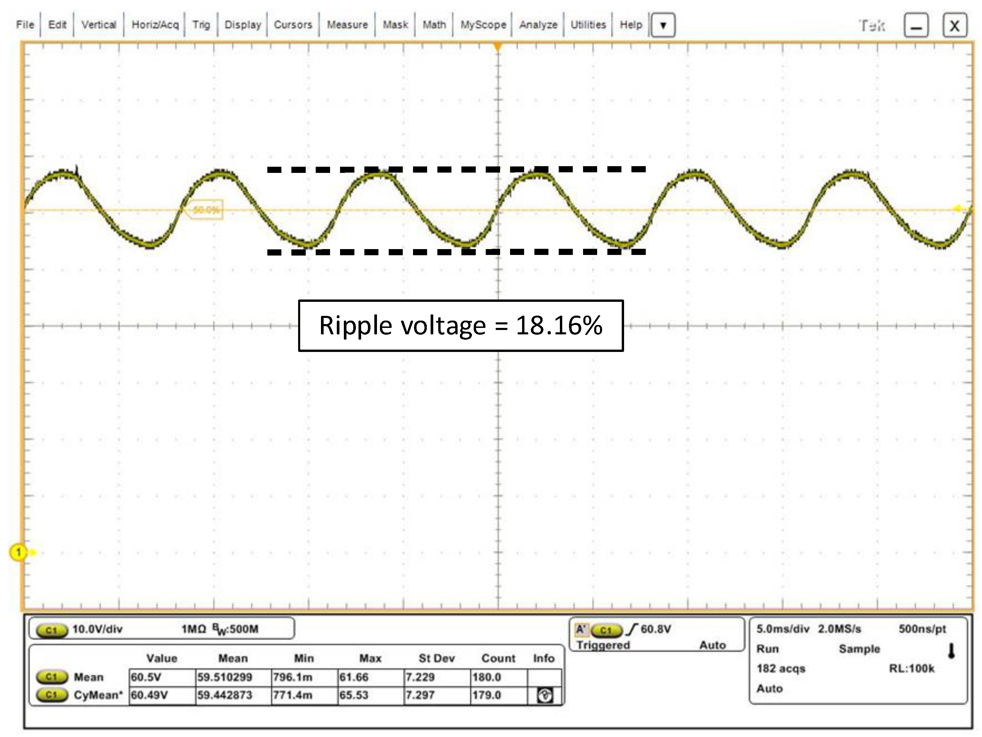
| Voltage ripple percentage | 16% | 14.86% | 18.16% |
| Average lamp current ILam | 160 mA | 159 mA | 163 mA |
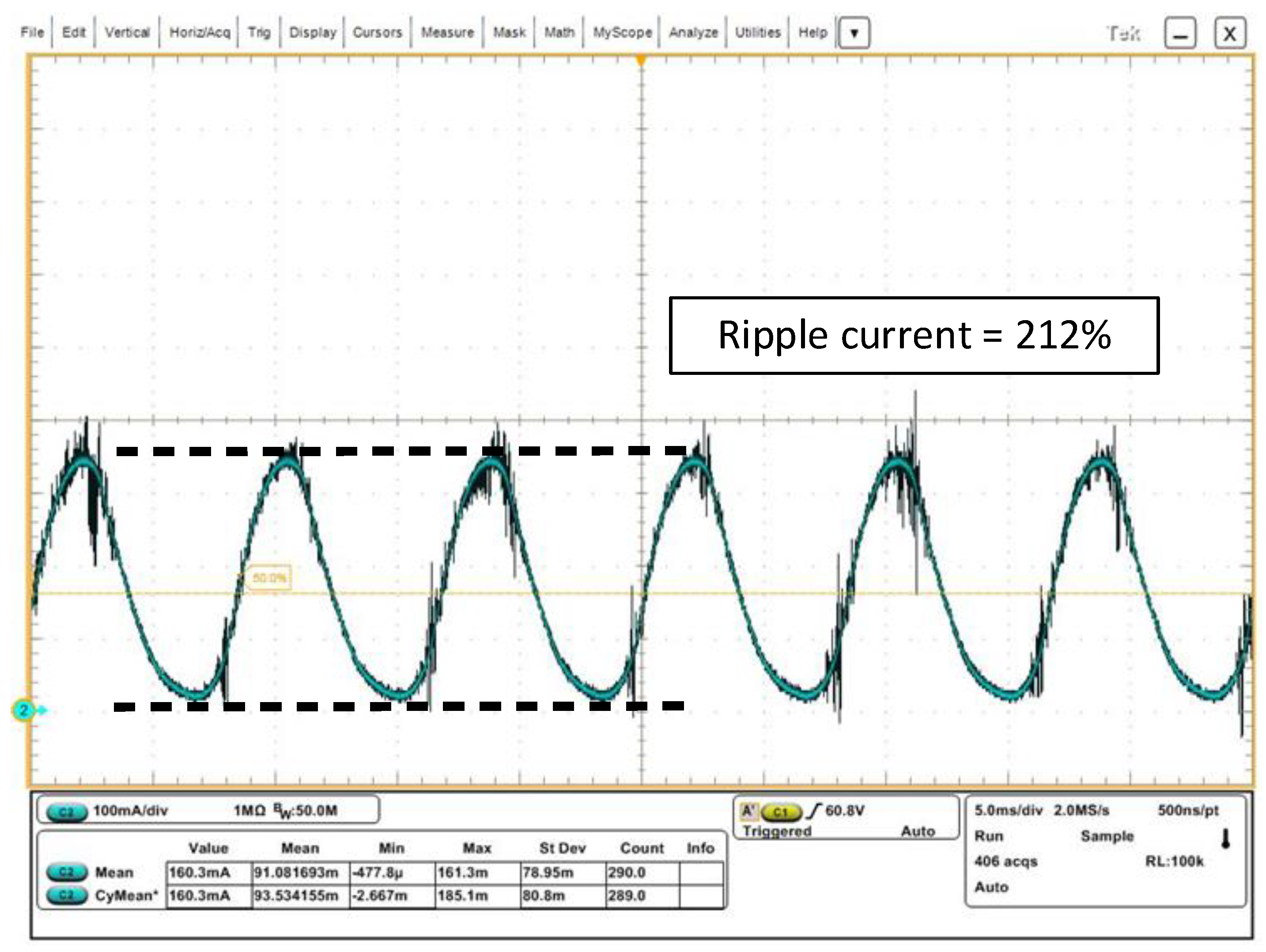
| Current ripple percentage | 0 | 194.8% | 212.1% |
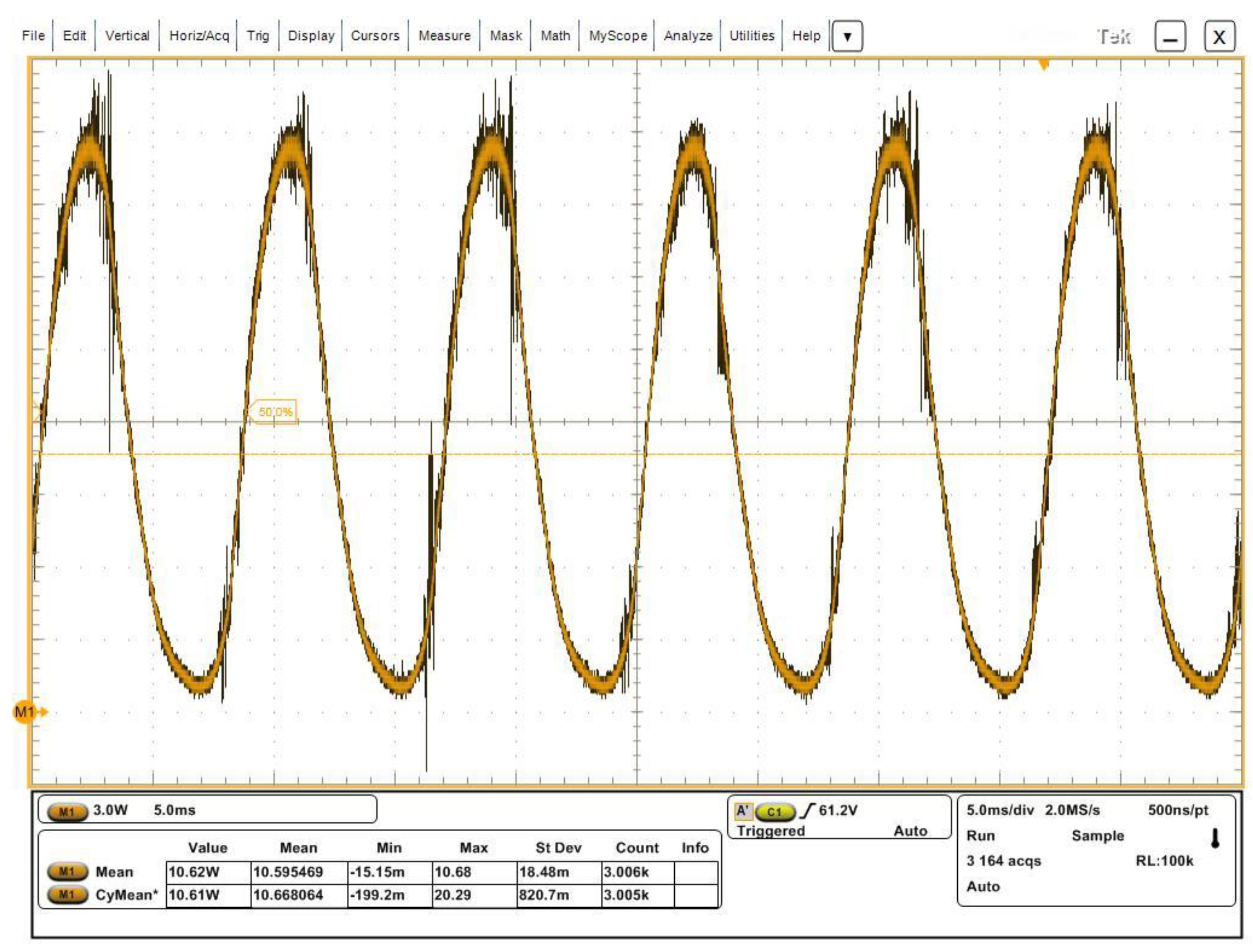
| Average lamp power PLam | 9.68 W | 9.62 W | 10.61 W |
| Average rectified power Pi | 9.68 W | 10.4 W | 11.55 W |
| Processed power Q | 60.96% | 61.5% | 62.94% |
| Flyback efficiency ɳF | 95% | 90% | 88% |
| Efficiency w/o bridge rectifier ɳT | 95% | 92.5% | 91.4% |
| Efficiency AC line-lamp ɳS | 95% | 90.8% | 88.79% |
| % Error | Ideal-Spice | Ideal-Prototype | Spice-Prototype |
|---|---|---|---|
| THDi | −15.85 | −3.89 | 14.21 |
| PF | 0.358 | −1.014 | −1.36 |
| Average lamp voltage VLam | 0.099 | 0 | −0.099 |
| Voltage ripple percentage | −7.25 | 13.3 | 22.2 |
| Average lamp current ILam | −0.625 | 0.18175 | 0.8176 |
| Current ripple percentage | - | - | 8.88% |
| Average lamp power PLam | −0.6198 | 9.607 | 10.29 |
| Average rectified power Pi | 7.43 | 19.3 | 11.05 |
| Processed power Q | 0.885 | 3.24 | 2.34 |
| Flyback efficiency ɳF | −5 | −7.36 | −2.2 |
| Efficiency w/o bridge rectifier ɳT | −2.63 | −3.78 | −1.189 |
| Efficiency AC line-lamp ɳS | −4.42 | −6.53 | −2.21 |
Publisher’s Note: MDPI stays neutral with regard to jurisdictional claims in published maps and institutional affiliations. |
© 2020 by the authors. Licensee MDPI, Basel, Switzerland. This article is an open access article distributed under the terms and conditions of the Creative Commons Attribution (CC BY) license (http://creativecommons.org/licenses/by/4.0/).
Share and Cite
Ponce-Silva, M.; Salazar-Pérez, D.; Rodríguez-Benítez, O.M.; Vela-Valdés, L.G.; Claudio-Sánchez, A.; De León-Aldaco, S.E.; Cortés-García, C.; Saavedra-Benítez, Y.I.; Lozoya-Ponce, R.E.; Aquí-Tapia, J.A. Flyback Converter for Solid-State Lighting Applications with Partial Energy Processing. Electronics 2021, 10, 60. https://doi.org/10.3390/electronics10010060
Ponce-Silva M, Salazar-Pérez D, Rodríguez-Benítez OM, Vela-Valdés LG, Claudio-Sánchez A, De León-Aldaco SE, Cortés-García C, Saavedra-Benítez YI, Lozoya-Ponce RE, Aquí-Tapia JA. Flyback Converter for Solid-State Lighting Applications with Partial Energy Processing. Electronics. 2021; 10(1):60. https://doi.org/10.3390/electronics10010060
Chicago/Turabian StylePonce-Silva, Mario, Daniel Salazar-Pérez, Oscar Miguel Rodríguez-Benítez, Luis Gerardo Vela-Valdés, Abraham Claudio-Sánchez, Susana Estefany De León-Aldaco, Claudia Cortés-García, Yesica Imelda Saavedra-Benítez, Ricardo Eliu Lozoya-Ponce, and Juan Antonio Aquí-Tapia. 2021. "Flyback Converter for Solid-State Lighting Applications with Partial Energy Processing" Electronics 10, no. 1: 60. https://doi.org/10.3390/electronics10010060
APA StylePonce-Silva, M., Salazar-Pérez, D., Rodríguez-Benítez, O. M., Vela-Valdés, L. G., Claudio-Sánchez, A., De León-Aldaco, S. E., Cortés-García, C., Saavedra-Benítez, Y. I., Lozoya-Ponce, R. E., & Aquí-Tapia, J. A. (2021). Flyback Converter for Solid-State Lighting Applications with Partial Energy Processing. Electronics, 10(1), 60. https://doi.org/10.3390/electronics10010060