Article

An Analysis and Modeling of the Class-E Inverter for ZVS/ZVDS at Any Duty Ratio with High Input Ripple Current

1
Department of Electrical and Electronic Engineering, Green University of Bangladesh, Dhaka 1207, Bangladesh
2
Department of Electrical and Computer Engineering, North South University, Dhaka 1229, Bangladesh
3
Department of Mechanical Engineering, Technical University of Denmark, 2800 Kgs. Lyngby, Denmark
4
Department of Electrical and Electronic Engineering, Swinburne University of Technology Malaysia, Sarawak 93350, Malaysia
5
Department of Electrical and Electronic Engineering, Aligarh Muslim University, Uttar Pradesh 202002, India
*
Author to whom correspondence should be addressed.
Electronics 2021, 10(11), 1312; https://doi.org/10.3390/electronics10111312
Submission received: 30 April 2021 / Revised: 23 May 2021 / Accepted: 25 May 2021 / Published: 30 May 2021
(This article belongs to the Section Power Electronics)

Abstract

:
This paper presents an analysis and modeling of the class-E inverter for ZVS/ZVDS execution at any duty ratio. The methodology is to determine the input current to the inverter analytically under the assumption that it always remains positive. The latter is ensured by proper selection of the input inductance such that the inverter always operates either in (1) the border condition mode or in (2) the continuous conduction mode regardless of the input ripple. Using this input current and applying the boundary conditions, the required input capacitance for the ZVS/ZVDS execution is determined at a specified input/output voltage, output power and load. The analysis shows that the ZVS/ZVDS can be achieved while the input capacitance is selected appropriately. A comparison between the analytical and simulation results is also formulated involving the proposed and other existing models. The simulation results that are provided at different duty ratios demonstrate that they are in a better agreement with the proposed analytical model regardless of the input inductance and the state of input ripple current. The analytical modeling is facilitated by using MAPLE®.

1. Introduction

The class-E inverter has found numerous applications in radio transmission, induction heating, industrial ultrasonic, renewable energy systems or commercial electronics industry [1,2,3,4,5]. In that regard, many application-specific designs are also proposed [3,4,5,6,7]. The widespread adoption of this inverter is mainly due to the compact topology with low component count and the capability of the circuit to deliver high power. On top of that, it can operate at high switching frequency with high efficiency if coupled with the zero-voltage switching (ZVS) or zero derivative voltage switching (ZVDS) techniques. The analysis and modeling of the ZVS/ZVDS class-E inverters are well reported in the literature [1,2,3,4,5,6,7,8,9,10,11,12,13,14,15,16]. Some of these modeling techniques are described here [1,2,8,11,12]. These techniques assume that the resonant current is sinusoidal, and, most importantly, the input current is a pure dc with very low ac component. The latter can be achieved if the input inductance is kept sufficiently large. Consequently, these models can define the behavior of the input current with the change in duty ratio. However, at lower inductances and higher ripple current, the assumption is no longer valid. The input current to the inverter is dependent on the input inductance, the input capacitance along with the duty ratio of the circuit. Consequently, the existing modeling techniques [1,2,3,4,5,6,7,8,9,12,13,14,15,16]. fail to define the input current accurately. This inaccuracy further leads to miscalculation of the input/output power and the efficiency of the circuit. Henceforth, this work proposes an input current–based modeling of the class-E inverter. This proposed modeling technique has the following key features:
(1) It provides an analysis and modeling of the class-E ZVS/ZVDS inverter for any duty ratio.
(2) More accurate modeling of the input current, regardless of the input inductance and input ripple current. This feature helps to determine the input power and efficiency more accurately.
(3) The model can ensure the ZVS/ZVDS operation at any given load.
In the following sections, this model is discussed, analyzed and compared with the simulated results. The analytical modeling presented is performed using MAPLE®.

2. The Circuit Operation of Class-E Inverter

The topology of the class-E inverter is given in Figure 1. The inductance Lr and the capacitance Cr is chosen to resonate at fr, which is also the switching frequency of the inverter. The Lf can be chosen to provide a constant dc current. However, the input ripple current percentage will increase with the decreasing size of the inductance Lf. The input capacitance Cin is inclusive of any parasitic drain to source capacitance of the switch and any external capacitance added. The switch S1 is operated with a duty ratio D. The switching pattern is given as follows.
S w i t c h = { T u r n e d   O N ,    0 θ < 2 π D T u r n e d   O F F ,    2 π D < θ < 2 π

2.1. Modes of Operation

The circuit is operated in two modes. In mode 1, the switch is turned ON and the voltage across the capacitor Cin falls to zero. The input current flows through the switch S1 and the Lf is charged. In the resonant tank, resonant current flows to the switch direction exchanging stored energy from Cr to Lr and completing half of the resonance cycle. This is shown in Figure 2a. In mode 2 (Figure 2b), the switch S1 is turned off and the input current Iin is diverted to the input capacitance Cin. At this moment, the input capacitor is charged to the peak switch voltage. Subsequently, it is discharged to zero at the end of this mode aiding in ZVS/ZVDS turn on of S1. If we assume the switch voltage is vs (θ), the following conditions must be satisfied in order to achieve ZVS or ZVDS:
v s ( 2 π ) = 0
and
d d θ v s ( 2 π ) = 0
The class-E inverter operating modes are shown in Figure 2. The current through the switch diverts to charge the input capacitor Cin when the switch is closed at θ = 2πD. As soon as Cin is charged completely, the current alters direction and Cin discharges. Due to the inductive effect of the resonant tank in Mode 2, the output current (Iout) lags the output voltage (Vout).

2.2. Assumptions

The circuit analysis is performed by applying the following assumptions.
  • All the components are ideal and do not possess any parasitic resistance or capacitances.
  • The switch is ideal. It is an open circuit (vs = ∞) while OFF and shorted (vs = 0) while ON.
  • The input current (Iin) is always positive.

3. The Circuit Modeling

3.1. Modeling Approach

Given,
N = L f L f _ b o u n d a r y
where, Lf_boundary = boundary value of the input inductor (Lf) while the inverter operates at the border condition mode (BCM) and N = inductance ratio.
Now, the modeling approach is stated as follows
  • Step 1: To determine the switch voltage (vs(θ))
  • Step 2: To apply the boundary conditions for ZVS/ZVDS and find input current (Iin(θ))
  • Step 3: To find Lf_boundary and the input ripple current (Δiin)
  • Step 4:
    • Case 1 (N ≈ 1)
      (1)
      To determine the average input current (Iin_avg_case1)
      (2)
      Using Iin_avg_case1 to find the input capacitance (Cin_case1)
    • Case 2 (1.5 < N < 3)
      (1)
      To determine the average input current (Iin_avg_case2)
      (2)
      Using Iin_avg_case2 to find the input capacitance (Cin_case2)
    • Case 3 (N ≥ 3)
      (1)
      To determine the average input current (Iin_avg_case3)
      (2)
      Using Iin_avg_case3 to find the input capacitance (Cin_case3)
  • Step 5: To find the peak switch voltage (vs_pk) and the peak switch current (is_pk)

3.2. The Derivation

3.2.1. Step 1

If the current through the input capacitor (Cin) is ICin, the switch voltage can be expressed as
v s ( θ ) = 1 ω C i n 2 π D θ I C i n d θ
From Figure 2a, the input current Iin can be written as
I i n ( θ ) = I C i n ( θ ) + I r ( θ )
where
  • Ir(θ) is the resonant current;
  • ICin is the capacitor current;
  • Iin(θ) is the input current.
From (1),
v s ( θ ) = 1 ω C i n 2 π D θ ( I i n _ a v g I m sin ( θ + φ ) ) d θ
Simplifying,
v s ( θ ) = 2 I i n _ a v g π D I m cos ( 2 π D + φ ) + I i n _ a v g θ + I m cos ( θ + φ ) ω C i n

3.2.2. Step 2

Applying v s ( 2 π ) = 0 for ZVS to (4),
I m = 2 π I i n _ a v g ( 1 D ) cos ( 2 π D + φ ) cos φ
or,
I i n _ a v g = I m ( cos ( 2 π D + φ ) cos φ ) 2 π ( 1 D )
Again, applying v s ( 2 π ) = 0 and using (5) and (6),
φ = π + arctan ( cos ( 2 π D ) 1 2 π ( 1 D ) + sin ( 2 π D ) )
Now, replacing (6) into (4) and simplifying (A1) (see Appendix A) is obtained. The output power to the load is defined by
P o u t , r m s = ( I m 2 ) 2 R L
or
I m = 2 P o u t , r m s R L
where RL is the given load resistance. Now, replacing Im from (9) into (7) and simplifying (A2) (see Appendix A) is obtained. The inductor vLf voltage can be expressed as
v L f ( θ ) = ω L f d d θ I i n ( θ )
Now,
v L f = { V i n   if   0 θ < 2 π D V i n v s ( θ )   if   2 π D θ θ
Now, considering the initial conditions, the current through Lf can be written as expressed in (A3) (see Appendix A). Now, fn (θ) can be written as
f n ( θ ) = 1 ω L f ( n 1 ) π θ V i n d θ
where (12) is extended in (A4) (see Appendix A). If n is odd and m is even, by generalizing, (A4) and (A5) (see Appendix A) can be obtained for n and m, respectively.

3.2.3. Step 3

The boundary value of the input inductor can be determined by the following:
Δ I i n = I i n ( 2 π D ) I i n ( 0 ) = 2 π D V i n ω L f _ b o u n d a r y
which gives
L f _ b o u n d a r y = 2 π D V i n ω Δ I i n
Now, the ripple current can be measured as
Δ I i n = I i n ( 2 π D ) I i n ( 2 π )
Substituting the values of Iin from (A4) and (A5) and simplifying, the following is obtained:
Δ I i n = 2 P o u t , r m s R L ( D 2 2 π D + π ) + 2 π ω V i n C i n ( D 1 ) ( 2 D 1 ) ( D 1 ) ω 2 C i n L f

3.2.4. Step 4

(a) 
Case 1: The input average current and the input capacitance for N ≈ 1
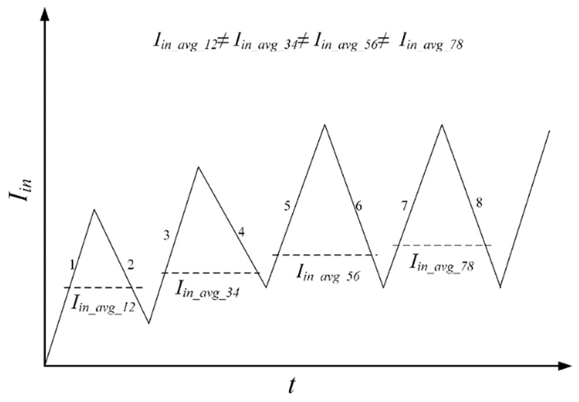
Now, if N ≈ 1, the current is always positive and the inverter operates in close proximity of the BCM with high ripple current. The theoretical input current waveform is shown in Figure 3. In this case, the average current can be defined as
I i n _ a v g _ c a s e 1 = 1 2 π ( 0 2 π D I i n _ 1 ( θ ) d θ + 2 π D 2 π I i n _ 2 ( θ ) d θ )
Now, simplifying (17) and using (A6)–(A8) can be obtained, which is shown in the Appendix A; where
A = 2 π ( D 1 ) cos φ ( 1 2 ) + sin φ
B = cos φ + π ( D 1 ) sin φ
C = sin φ π ( D 1 ) cos φ
Again, from (3), (A9) (see Appendix A) is obtained. Alternatively, the average current (Iin_avg_case1_alt) can be found (while n = 5 and m = 6) as shown in (A10) (see Appendix A). Accordingly, solving and simplifying (A10), (A11) (see Appendix A) is obtained, where
A = π ( D + 3 ) cos φ sin φ
B = cos φ + π ( D + 3 ) sin φ
Now, the output power of the converter is
P o u t , r m s = ( I m 2 ) 2 R L = ( V o u t , p e a k 2 ) 2 R L
Now, Im from (9) for case 1 is
I m = 2 π I i n _ a v g _ c a s e 1 ( 1 D ) cos ( 2 π D + φ ) cos φ
Replacing from (19) in (18), Pout,rma is obtained as demonstrated in (A12) (see Appendix A). Then, (A12) is solved for Cin, where N1 and D1 are demonstrated in (A13) and (A14) (see Appendix A).
C i n _ c a s e 1 = N 1 D 1
The negative quotient of Cin_case1 is neglected.
(b) 
Case 2: The input average current and the input capacitance for 1.5 < N < 3:
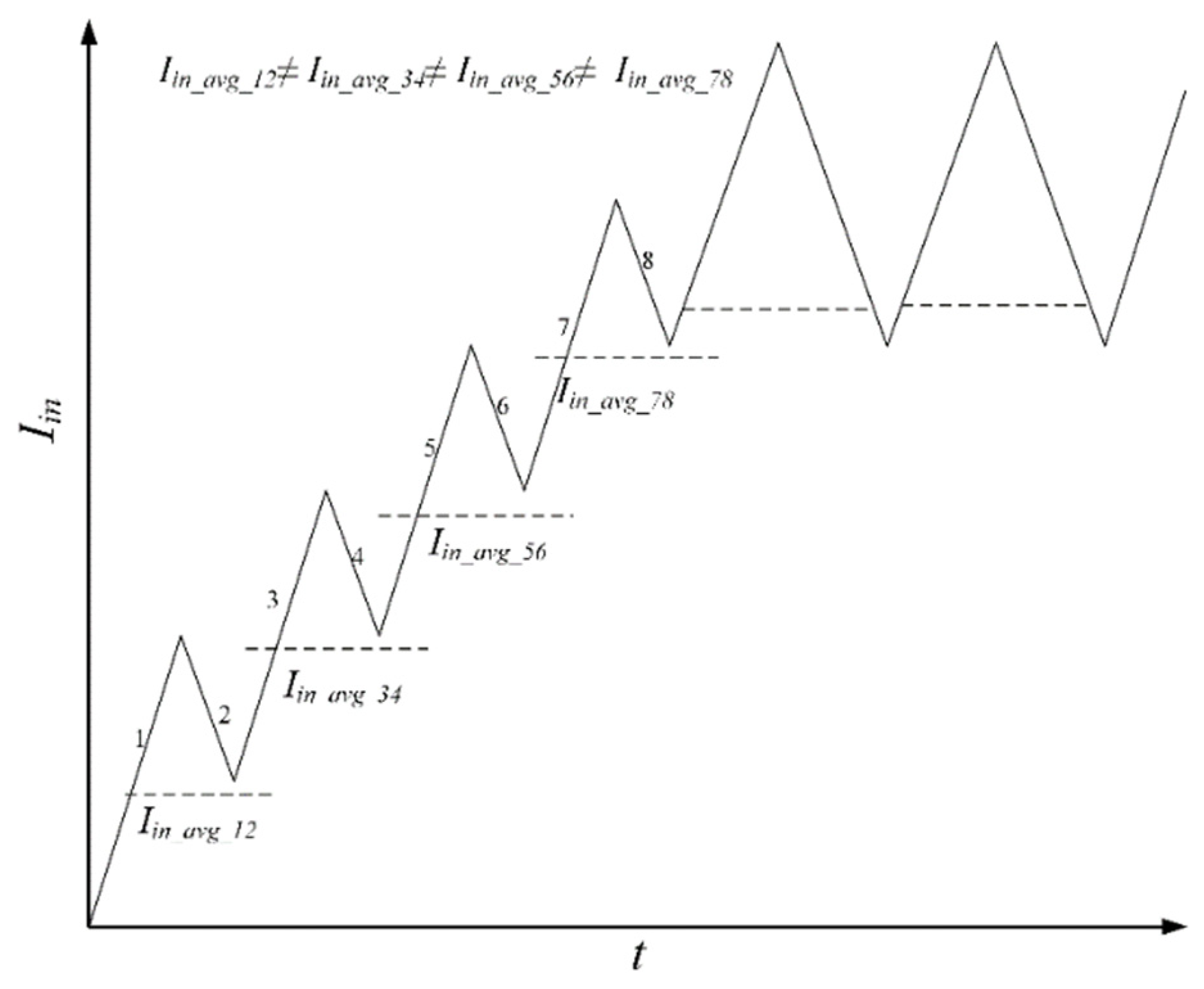
In this case, the input inductor is slightly greater than the Lf_boundary (approximately 1.5 to 2.5 times of Lf_boundary). The Lf_boundary, which is calculated from (14), is 50 µH and 55 µH at D = 0.55 and 0.50, respectively. The theoretical input current waveform is shown in Figure 4. The current is always positive and the inverter operates at the continuous conduction mode (CCM) with high current ripple. The average current Iin_avg_case_alt as derived in (29) is appropriate. However, due to the transient nature of the input current, Iin_avg_sum34 is determined to define the input current more accurately.
For a better understanding, Iin_avg_78 is derived in (A15), where
A = π ( D + 3 ) cos φ sin φ B = cos φ + π ( D + 3 ) sin φ
The current is shown in Figure 5. Now, using (21) and (A16) (see Appendix A) is solved for Cin as demonstrated in (A17) (see Appendix A). The negative quotient of Cin_case2 is neglected.
(c) 
Case 3-The input average current and the input capacitance for N ≥ 3:
In this case, the input inductor is greater than the Lf_boundary (approximately 3 to 5 times of Lf_boundary). The Lf_boundary, which is calculated from (14), is 50 µH and 55 µH at D = 0.55 and 0.50, respectively. The theoretical input current waveform is shown in Figure 5. The current is always positive and the inverter operates at the continuous conduction mode (CCM) with low current ripple. Moreover, in this case, Iin_avg_case2 is sufficient. However, Iin_avg_15-16 is determined to define the input current more accurately. The Cin_case3 is shown in (A20).
Hence,
I i n _ a v g _ c a s e 3 = I i n _ a v g _ c a s e 2 = I i n _ a v g _ 78
I i n _ a v g _ c a s e 3 _ a l t = I i n _ a v g _ 15 16
Replacing values in (22) and simplifying, (A18) (see Appendix A) is obtained.

3.2.5. Step 5

The switch voltage can be determined from (3), (6) and (9). Now, if n = 6, solving for dvs/ = 0,
θ p k = φ arcsin ( 1 2 π ( D 1 ) )
Replacing θpk from (23) into (A19) (see Appendix A) gives the peak switch voltage,
v s _ p k = 1 2 π ω C i n ( D 1 ) 2 P o u t , r m s R L ( ( 4 π 2 ( D 1 ) 2 1 ) + arcsin ( 1 2 π ( D 1 ) ) + φ )
The switch current,
I S ( θ ) = I i n I m sin ( θ + φ )
Replacing Iin from (5),
I S ( θ ) = I m ( cos ( 2 π D + φ ) cos φ ) 2 π ( 1 D ) I m sin ( θ + φ )
The current peaks at
θ = 2 π D
Hence, replacing from (23) and (24) in (26),
i s _ p k = 2 P o u t , r m s R L ( π ( D 1 ) sin ( 2 π D + φ ) cos φ 2 + cos ( 2 π D + φ ) 2 ) π ( D 1 )

4. Analysis of The Model Parameters

4.1. The Phase Difference (φ):

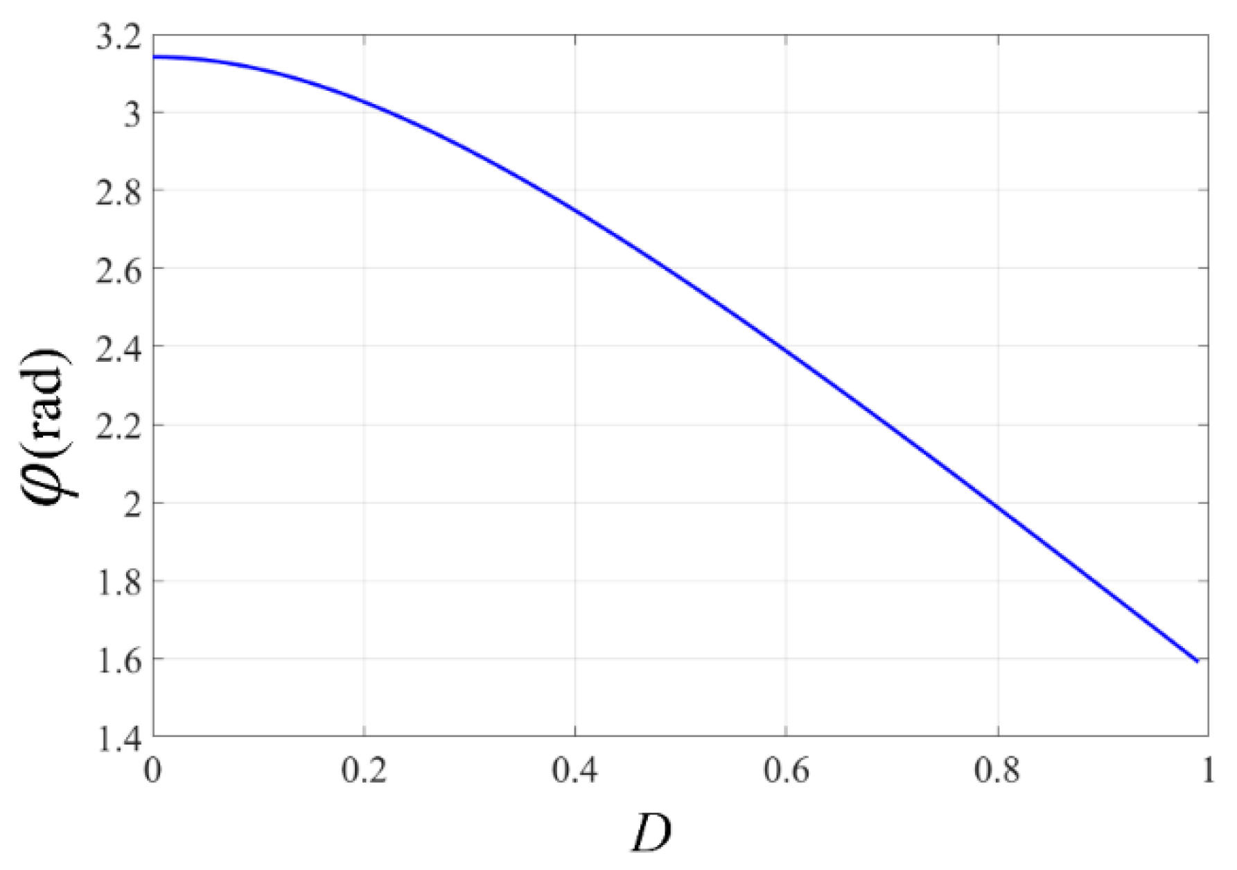
The phase difference between the output voltage and current is given in (8). Now, if D = 0, φ = π . Again, if D = 1, φ is undefined (0/0).
In Figure 6, φ is plotted against D. At D = 0, φ is maximum at π. As D increases, the phase difference decreases.

4.2. The Input Current Ripple

The input current ripple decreases with increasing size of Lf.
In Figure 7, the input current ripple percentage is demonstrated against Lf. As Lf decreases, the ripple percentage increases according to (13). However, the input current (Iin) remains positive as long as Lf > Lf_boundary.

4.3. The Input Capacitance (Cin)

4.3.1. Case 1

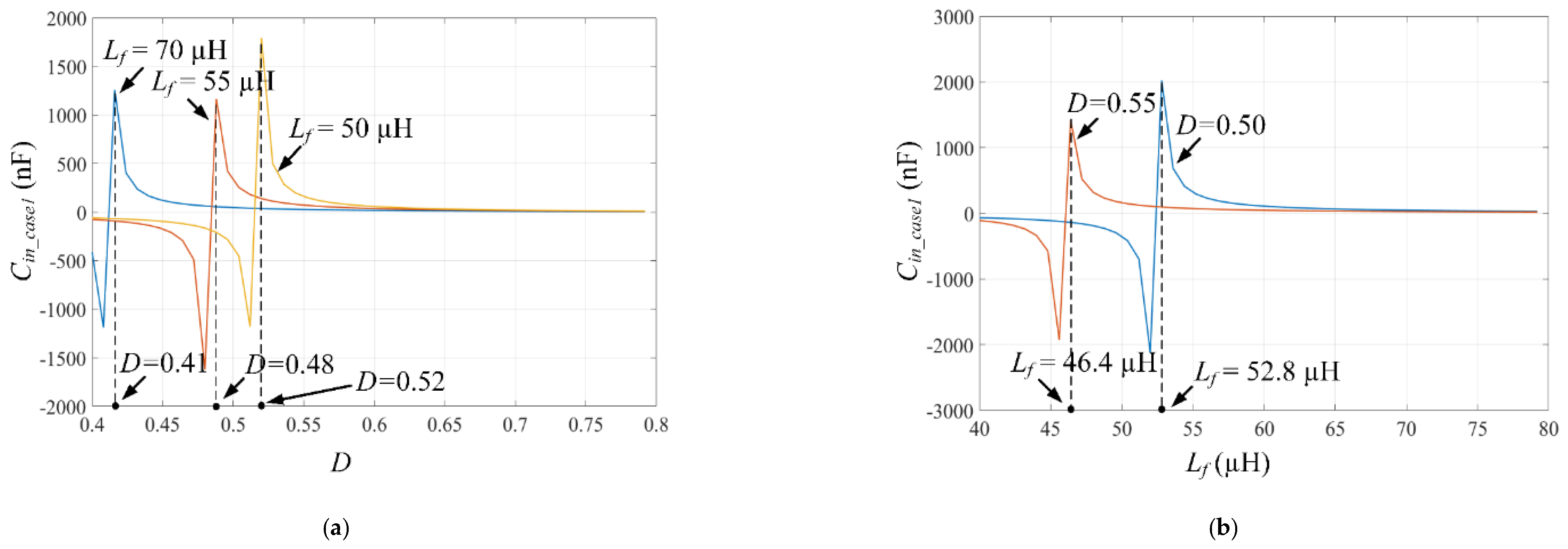
In Figure 8a,b, Cin_case1 is plotted against D and Lf, respectively, while Vin = 15 V, Vout_peak = 20 V, Pout_rms = 10 W and fs = 150 kHz. As obvious from Figure 9a, Cin_case1 is always positive for Dcr ≥ 0.52, Dcr ≥ 0.48 and Dcr ≥ 0.41, while Lf = 50, 55 and 70 µH, respectively. In Figure 8b, Cin_case1 is positive for Lf_cr > 52.8 and Lf_cr > 46.4 for D = 0.55 and 0.50, respectively. To achieve ZVS/ZVDS, these critical duty ratio and input inductances have to be maintained with Cin_case1 being chosen appropriately under the specified conditions.

4.3.2. Case 2

In Figure 9a,b, Cin_case2 is plotted against D and Lf, respectively, while Vin = 15 V, Vout_peak = 20 V, Pout_rms = 10 W and fs = 150 kHz. As obvious from Figure 10a, Cin_case2 is always positive for Dcr ≥ 0.52, Dcr ≥ 0.54 and Dcr ≥ 0.60, while Lf = 100, 90 and 80 µH, respectively. In Figure 9b, Cin_case2 is positive for Lf_c > 92.5 and Lf_cr > 105.2 for D = 0.55 and 0.50, respectively. To achieve ZVS/ZVDS, these critical duty ratio and input inductances have to be maintained with Cin_case1 being chosen appropriately under the specified conditions.

4.3.3. Case 3

In Figure 10a,b, Cin_case3 is plotted against D and Lf, respectively, while Vin = 15 V, Vout_peak = 20 V, Pout_rms = 10 W and fs = 150 kHz. As obvious from Figure 10a, Cin_case3 is always positive for Dcr ≥ 0.48, Dcr ≥ 0.52 and Dcr ≥ 0.61, while Lf = 170, 150 and 120 µH, respectively. In Figure 10b, Cin_case2 is positive for Lf_cr > 138.2 and Lf_cr > 159 at D = 0.55 and 0.50, respectively. To achieve ZVS/ZVDS, these critical duty ratio and input inductances have to be maintained with Cin_case3 being chosen appropriately under the specified conditions.

4.4. Peak Switch Voltage (Vs-pk)

The peak switch voltage (vs_pk) from (24) is demonstrated in Figure 11. The rating of the switch should be 2–3 times the peak voltage for safe operation under the specified operating conditions. Moreover, from Figure 12b, it is obvious that the peak switch voltage can be lowered by lowering the output power at a given D and RL. Similarly, it can be lowered by lowering the RL at a given D and Pout_rms as obvious from Figure 12c. However, for both cases, the output voltage is also affected with vs_pk.

4.5. Peak Switch Current (is-pk)

The peak switch current (is_pk) from (28) is demonstrated in Figure 12. The peak current has a maximum in the mid region of D (0.3 to 0.5) and gradually decreases on both sides. Hence, given the optimum D = 0.5, the rating of the switch should be 2–3 times the peak current for safe operation.

5. Simulation and Experimental Verification

The class-E inverter is simulated in MATLAB Simulink environment to demonstrate the waveforms. Table 1 demonstrates the common parametric values.
The Lr and Cr is selected to maintain a high loaded QL factor (QL ≥ 10), which is given as
Q L = ω L r R L
Hence, the resonance frequency of the circuit is
f r = 1 2 π L r C r
Once, Lr is selected for the desired QL from (46), Cr can be determined.
In this case, the input inductor is equal or close to the Lf_boundary. The Lf_boundary, which is calculated from (14), is 50 µH and 55 µH at D = 0.55 and 0.50, respectively. The output voltage and power of the inverter should demonstrate the specified value with minimal error. In addition, the average input current from the simulation must concur with the analytical value from (A8). Accordingly, as Cin is implemented calculated from (A17), the ZVS/ZVDS should be executed.
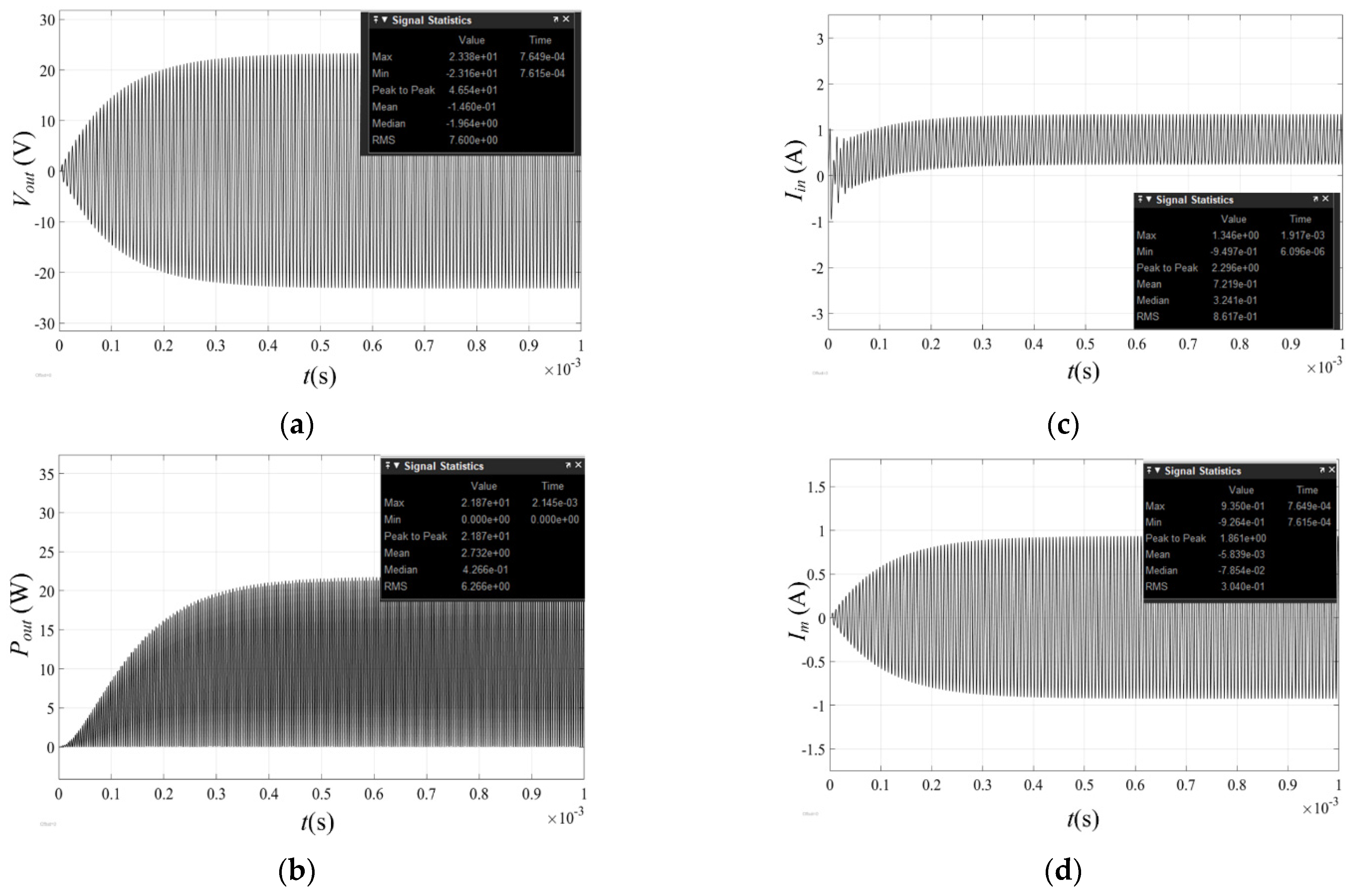
The circuit is simulated at the designated parametric values stated in Table 1. The output voltage and power waveforms are shown in Figure 13 for D = 0.50. As opposed to the ideal lossless analytical model, the switch in the simulation induces a conduction loss across the ON resistance (Rds-ON = 0.015 Ω).
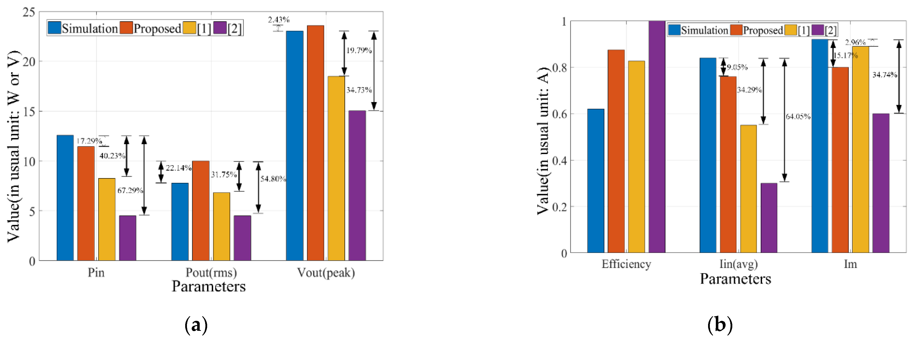
In Figure 14, the analytical values of Vin, Vout, Pin, Pout, η, Iin_avg, Im from the proposed model and [1,2] are stated along with the simulated results for D = 0.55 and 0.50. The percentage differences between the analytical and simulation results are calculated.
In Figure 14a, at D = 0.55, Vout_peak and Pin from the proposed model demonstrate a difference of 2.43% and 17.29% with the simulated value, respectively. For [1], these differences are maximum at 24.85% and 67.29%, respectively. In Figure 14b, the proposed model demonstrates a difference of 9.05% and 15.17% for Iin_avg and Im while the maximum is 64.05% and 34.74%, respectively, for [1].
In Figure 14c, at D = 0.50, Pin, Pout_rms and Vout_peak demonstrate a difference of 10.25, 37.34 and 16.90%, respectively, for the proposed model. These parameters demonstrate a maximum difference of 52.03, 48.09 and 19.45%, respectively, for [1]. Again, in Figure 14d, a maximum difference of 52.07% in Iin_avg and 31.11% in Im are observed for [1]. However, Iin_avg and Im are most accurately determined by the proposed model and [2] demonstrating an error of 9.25% and 4.38%, respectively.
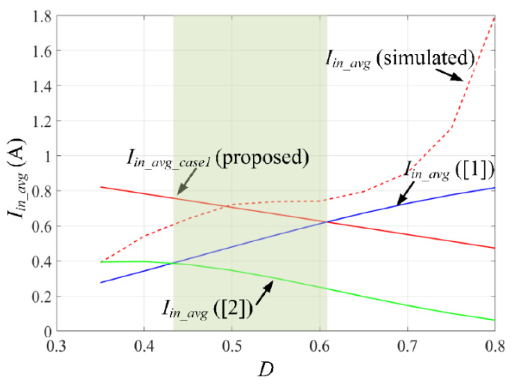
In Figure 15, the input average current for the proposed model, the model in [1,2] and for the simulation is demonstrated against D. As obvious, the optimum operating condition for the proposed model is D ≈ 0.43 to 0.61. The shaded area stands for an error ≤10%.
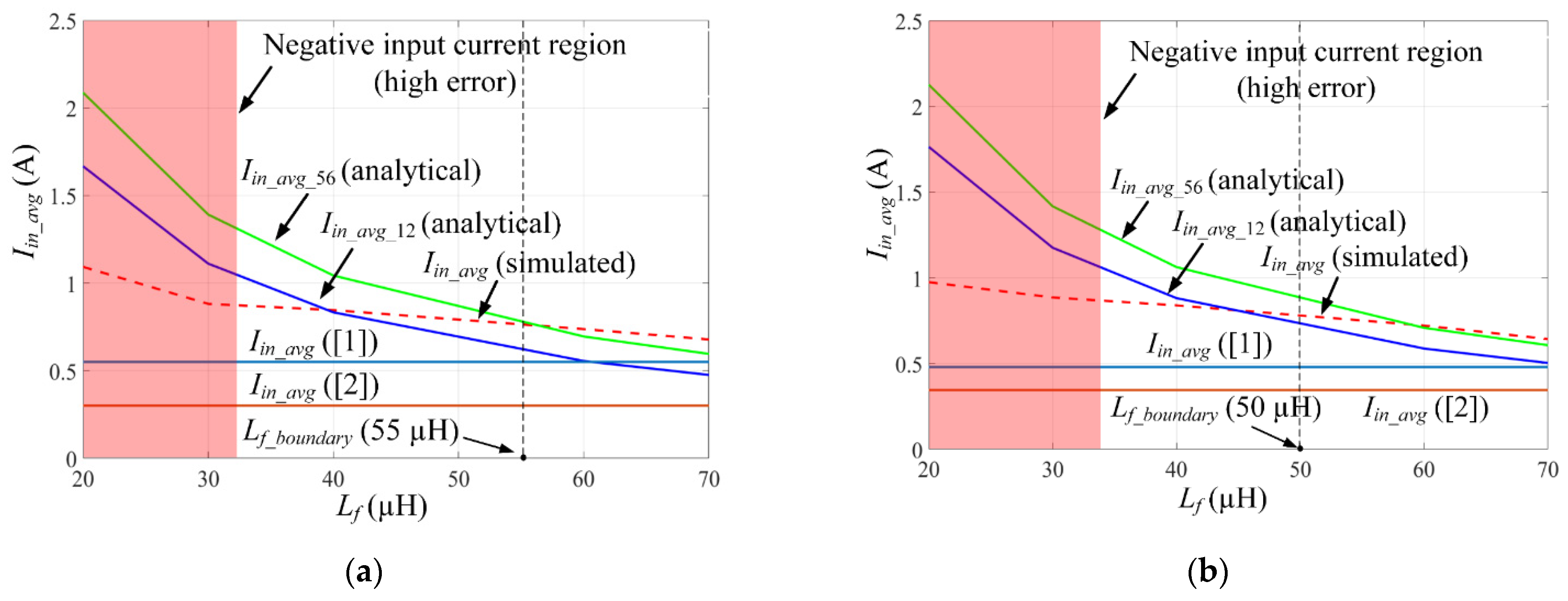
As stated previously, this model is accurate when the input inductor is equal or close to the boundary value (Lf_boundary). Hence, the analytical value of Iin should closely match to that from the simulation. In Figure 16, the input average current for the proposed model is compared with [1,2] and the simulation against D. The results are summarized in Table 2. As obvious, the percentage error between the analytical and simulated values are maximum when the input current is negative (at low Lf). As Lf approaches to Lf_boundary, the current always remains positive. Subsequently, the error is minimized.
As Lf continues to increase from Lf_boundary, Iin_avg_56 provides better approximation than Iin_avg_12. This is because of the transient nature of the current when the switch is turned ON. The error is as low as 1.5% (for Iin_avg_12) near Lf_boundary and 3.10% (for Iin_avg_56) at higher inductances. This is graphically shown in Figure 16a,b where the high error region (>20%) is shaded for D = 0.55 and D = 0.50, respectively. Accordingly, this region falls out of the scope of this model because of a significant error in approximating the average input current.

5.1. Case-2: The Continuous Conduction Mode (1 < N < 3)

As stated earlier, the input inductor is slightly greater than the Lf_boundary (approximately 1.5 to 2.5 times of Lf_boundary). The analytical values of Vout, Pout, Iin_avg and Im are derived in Section 3.2. In this section, the average input current for the proposed model as stated in (A15) is calculated and compared with the simulation results.
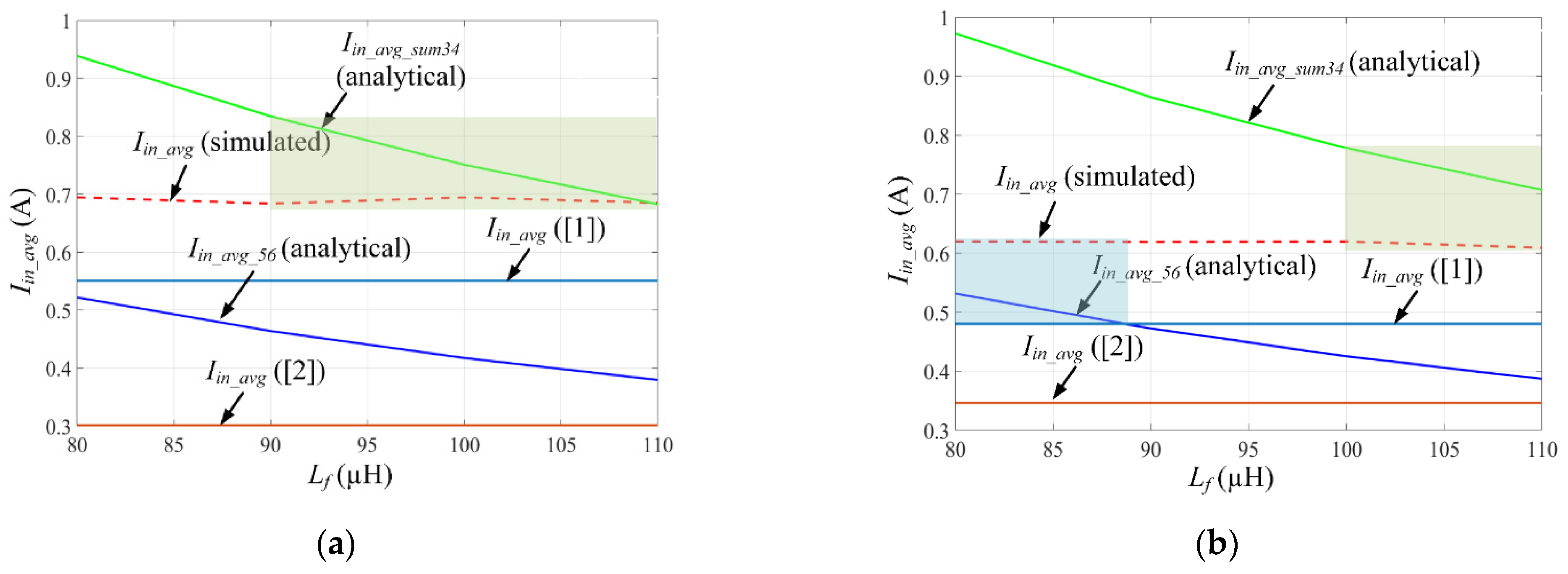
In Figure 17, the input average current for the proposed model, the model in [1,2] and for the simulation is demonstrated against D. The optimum operating condition for the proposed model is D ≈ 0.50 to 0.63. The shaded area stands for an error ≤10%.
In Figure 18, the input average current for the proposed model is compared with [1,2] and the simulation against D. The analytical and simulation results are summarized in Table 3. Owing to the transient nature of the input current, Iin_avg_56 gives rise to significant error in tracking the simulated values. The error becomes maximum, i.e., 44% and 36% at D = 0.55 and 0.50, respectively, for Lf = 110 µH. However, Iin_avg_sum34 provides a better approximation of the input current as Lf continues to increase. The minimum error of 0.36% and 16 % is recorded at D = 0.55 and 0.50, respectively, for Lf = 110 µH. The results are graphically shown in Figure 18a,b where the lower error region (≤10%) is shaded.

5.2. Case-3: The Continuous Conduction Mode (N > 3)

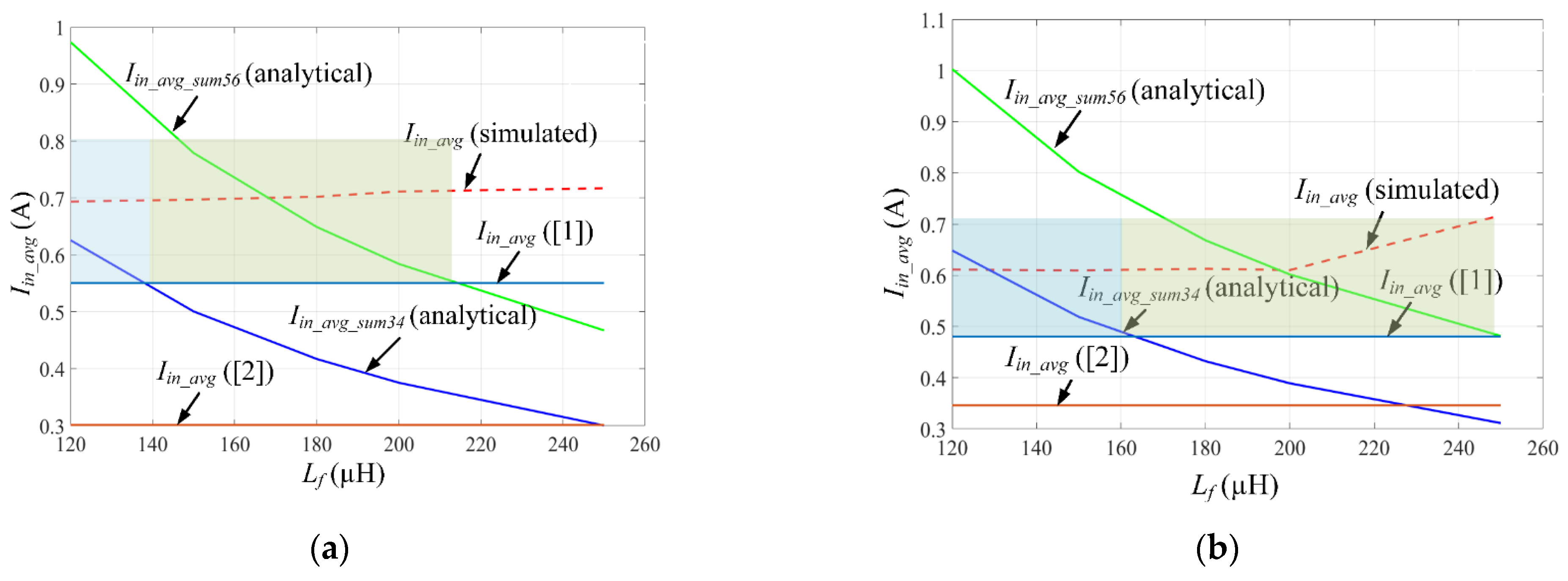
For case 3, the input inductor is greater than the Lf_boundary (approximately 2.5 to 5 times of Lf_boundary). The analytical values of Vout, Pout, Iin_avg and Im are derived in Section 3.2. In this section, the average input current for the proposed model as stated in (A19) is calculated and compared with the simulation results. In Figure 19, the input average current for the proposed model, the model in [1,2] and for the simulation is demonstrated against D. The optimum operating condition for the proposed model is D ≈ 0.50 to 0.63. The shaded area stands for an error ≤10%.
In Figure 20, the input average current for the proposed model is compared with [1,2] and the simulation against D. The analytical and simulation results are summarized in Table 4. Owing to the transient nature of the input current, Iin_avg_sum34 gives rise to significant error in tracking the simulated values at Lf = 160 µH. Beyond the latter, Iin_avg_sum56 provides a better approximation of the input current than [1,2] as Lf continues to increase. The minimum error of 7.56% and 1.39% is recorded at D = 0.55, Lf = 180 and D = 0.50, Lf = 200, respectively. The results are graphically shown in Figure 20a,b where the lower error region (≤10%) is shaded.
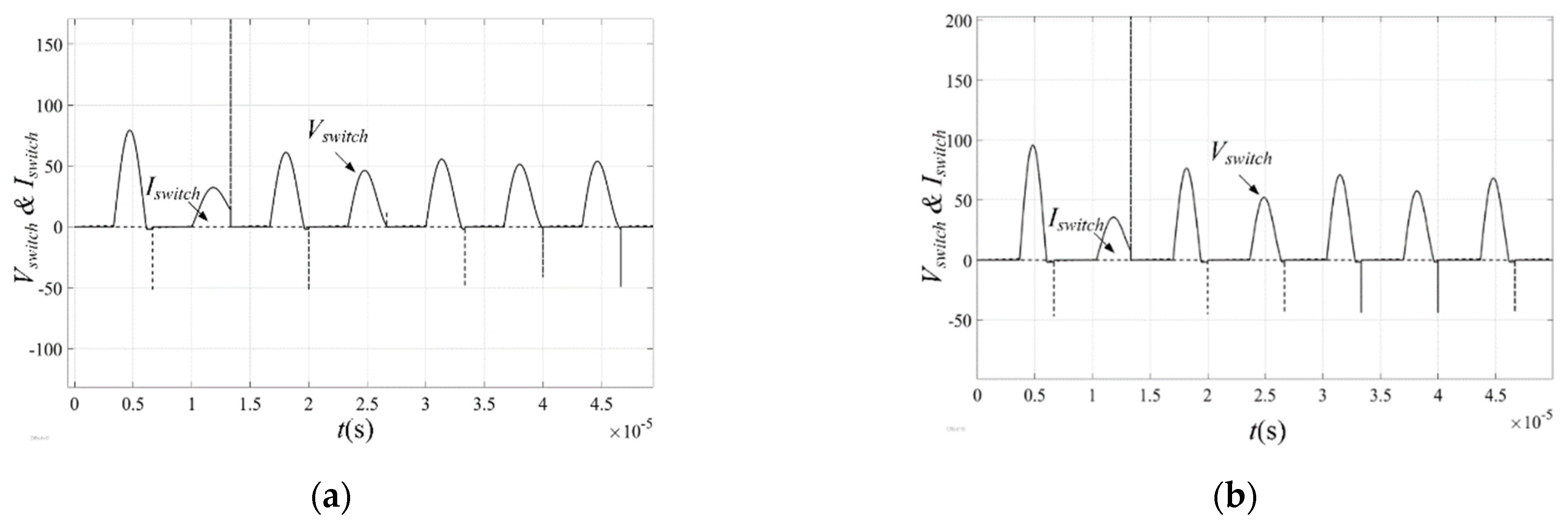
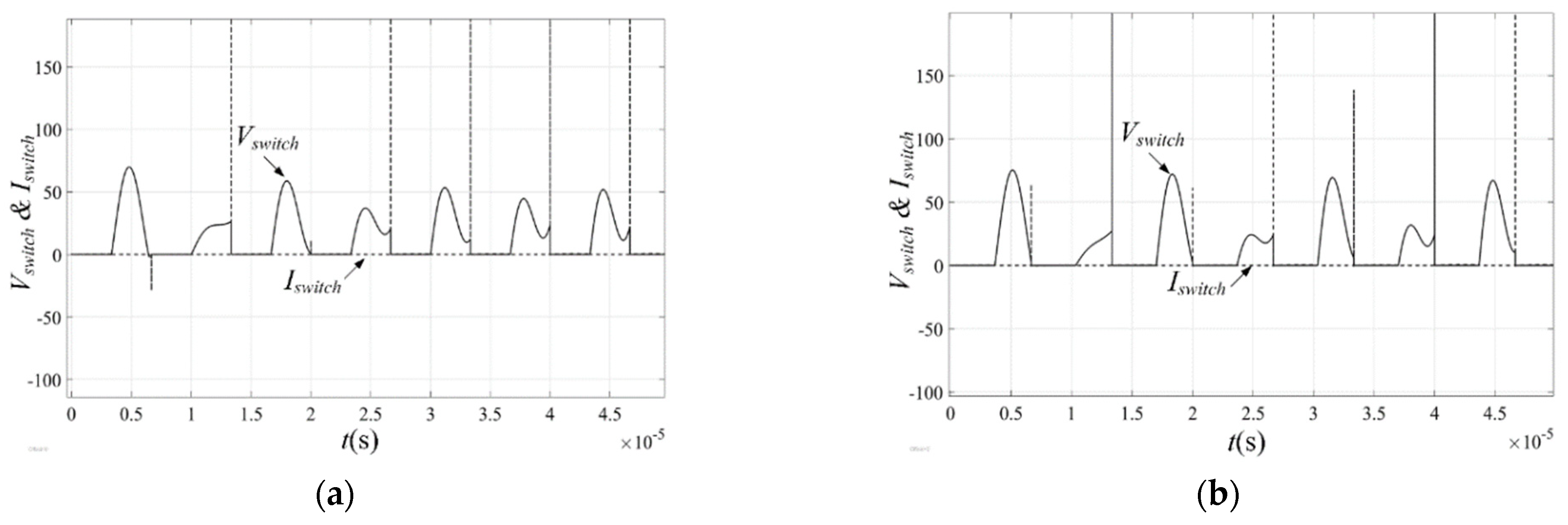
The switch voltage and current waveforms are shown in Figure 21a,b for D = 0.50 and 0.55, respectively, for case 1. As expected, the switch voltage is either zero or negative at constant dvs/dt. In Figure 21, the switch voltage and current waveforms are multiplied to measure the turn off losses. However, the exact switching loss would be nearly impossible to calculate from both a theoretical and simulation perspective. Instead, a very accurate relative estimate has been made from the simulated waveforms. As observed, the turn off loss (Pswitching_loss_rms) is approximately 0.72, 1.2 and 1.93% of the output power (Pout_rms = 7.786 W) for D = 0.50 and 0.55, respectively. In all cases, the turn on loss is negligible. The results are accumulated in Table 5 below.
The switch voltage and current waveforms are shown in Figure 22a,b for D = 0.50 and 0.55, respectively, for case 2. As expected, the switch voltage is either zero or negative at constant dvs/dt. In Figure 22, the switch voltage and current waveforms are multiplied to measure the turn off losses. As observed, the turn off loss (Pswitching_loss_rms) is approximately 0.60, 1.08 and 1.52% of the output power (Pout_rms = 7.786 W) for D = 0.50 and 0.55, respectively. In all cases, the turn on loss is negligible. The results are accumulated in Table 5.
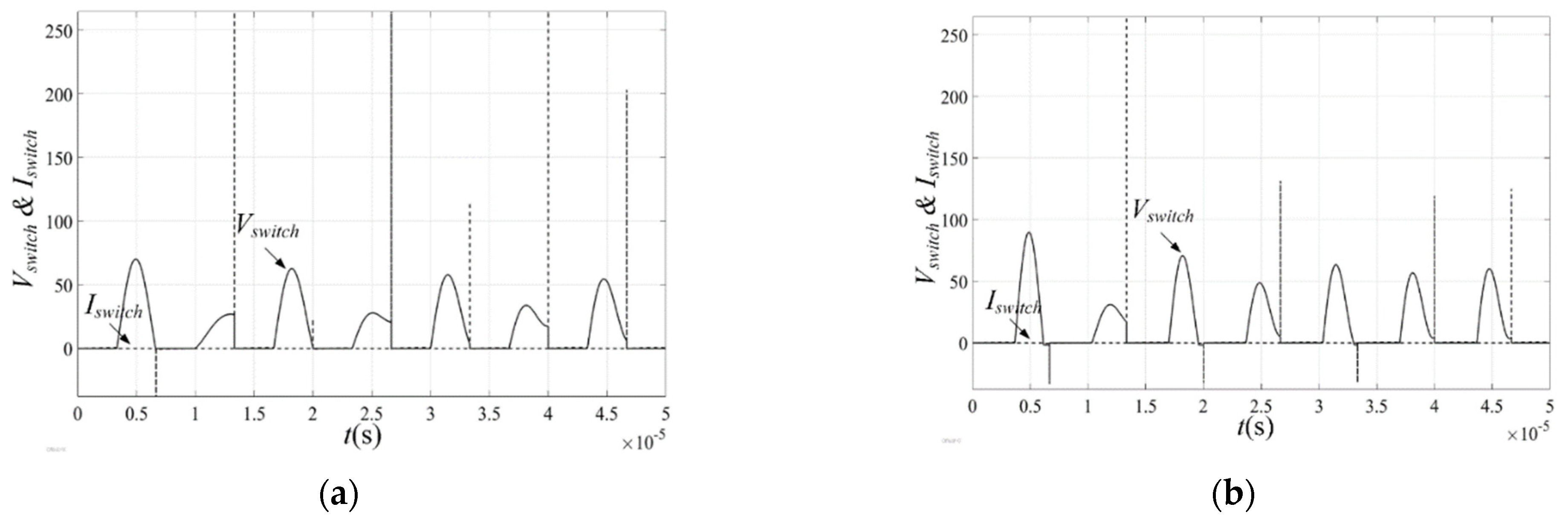
The switch voltage and current waveforms are shown in Figure 23a,b for D = 0.50, 0.55 and 0.60, respectively, for case 3. As expected, the switch voltage is either zero or negative at constant dvs/dt. In Figure 23, the switch voltage and current waveforms are multiplied to measure the turn off losses. As observed, the turn off loss (Pswitching_loss_rms) is approximately 0.56, 0.20 and 1.27 % of the output power (Pout_rms = 7.786 W) for D = 0.50 and 0.55, respectively. In all cases, the turn on loss is negligible. The results are accumulated in Table 5 below.
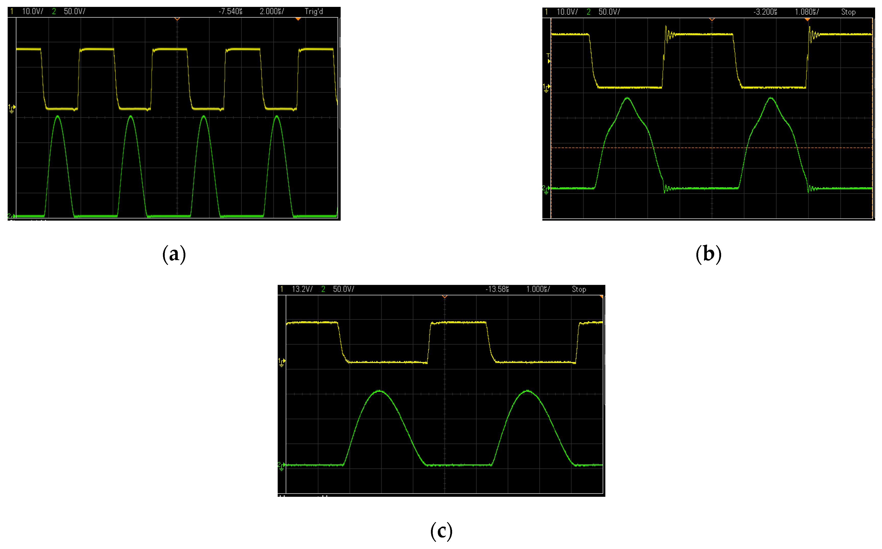
In Figure 24, the switching waveforms reconfirms the ZVS achievement for case 1, 2 and 3.

6. Conclusions

In this paper, the class-E inverter is modeled and analyzed for ZVS/ZVDS implementation. The modeling is based upon determining the input current to the inverter for various input inductances and state of ripple current under a specified condition. A comprehensive simulation and experimental testing are performed to support the proposed analytical model. Eventually, as opposed to the existing models, the proposed model can determine the input current, input/output power, efficiency more accurately. The percentage of error is also determined for different size of the input inductor and the duty ratio. For most of the part, the percentage error increases with increasing input inductor size at higher duty ratio and decreases at lower duty ratio. This input current is also used to determine the input capacitance of the inverter to aid the ZVS/ZVDS execution. It is observed that the percentage loss is <2% for all cases. In general, the results demonstrate that the proposed model is in better agreement with the test results as compared with the other existing models regardless of the input inductance and the input ripple current.

Author Contributions

Conceptualization, R.H.A.; data curation, M.H.M. and M.A.u.H.; formal analysis, A.S.M.S. (A. S. M. Shihavuddin), M.M.K. and J.A.; funding acquisition, A.I.; investigation, M.M.K. and M.S.B.A.; methodology, R.H.A. and J.A.; project administration, A.S.M.S. (A. S. M. Shihavuddin) and A.A.M.; resources, M.S.B.A. and A.S. (Ashraf Siddiquee); software, M.H.M.; validation, R.H.A.; visualization, R.H.A. and A.S. (Ashraf Siddiquee); writing—original draft, R.H.A.; writing—review and editing, A.A.M., M.A.u.H. and A.S. (Ashraf Siddiquee). All authors have read and agreed to the published version of the manuscript.

Funding

This research received no external funding. The APC was funded by Aminul Islam, from DTU, Lyngby, Denmark and ASM Shihavuddin from Green University of Bangladesh.

Conflicts of Interest

The authors declare no conflict of interest.

Appendix A

v s ( θ ) = I m ( cos ( 2 π D + φ ) cos φ ) ( 2 π D θ ) 2 π I m ( cos ( 2 π D + φ ) cos ( θ + φ ) ) ( D 1 ) 2 π ω C i n ( D 1 )
v s ( θ ) = 2 P o u t , r m s R L ( ( 2 π D θ ) ( cos ( 2 π D + φ ) cos φ ) 2 π ( D 1 ) ( cos ( 2 π D + φ ) cos ( θ + φ ) ) ) 2 π ω C i n ( D 1 )
I i n _ 1 ( θ ) = f 1 ( θ ) + 0 I i n _ 2 ( θ ) = f 2 ( θ ) + I i n _ 1 ( 2 π D ) = f 2 ( θ ) + f 1 ( 2 π D ) + 0 I i n _ 3 ( θ ) = f 3 ( θ ) + I i n _ 2 ( 2 π ) = f 3 ( θ ) + f 2 ( 2 π ) + f 1 ( 2 π D ) + 0 I i n _ 4 ( θ ) = f 4 ( θ ) + I i n _ 3 ( 2 π ( 1 + D ) ) = f 4 ( θ ) + f 3 ( 2 π ( 1 + D ) ) + f 2 ( 2 π ) + f 1 ( 2 π D ) + 0 I i n _ 5 ( θ ) = f 5 ( θ ) + I i n _ 4 ( 4 π ) = f 5 ( θ ) + f 4 ( 4 π ) + f 3 ( 2 π ( 1 + D ) ) + f 2 ( 2 π ) + f 1 ( 2 π D ) + 0
f n ( θ ) = 1 ω L f ( n 1 ) π θ V i n d θ
f m ( θ ) = 1 ω L f 2 π ( m 2 2 + D ) θ ( V i n ( 1 ( D 1 ) π ω C i n ( ( ( π θ 2 ) cos ( 2 π D + φ ) + π ( D 1 ) cos ( θ + φ ) ( π D θ 2 ) cos φ ) P o u t , r m s R L ) ) ) d θ
I i n _ n ( θ ) = f n ( θ ) + f m ( π ( n 1 ) ) + f n 2 ( 2 π ( n 3 2 + D ) ) + f m ( π ( n 3 ) ) + ..........
I i n _ m ( θ ) = f m ( θ ) + f n ( 2 π ( ( m 1 ) 1 2 + D ) ) + f m 2 ( π ( m 2 ) ) + f n ( 2 π ( ( m 3 ) 1 2 + D ) ) + ........
I i n _ a v g _ c a s e 1 = 1 ω 2 L f C i n ( 2 P o u t , r m s R L ( 1 D ) ( A cos 2 ( π D ) + 2 B cos ( π D ) sin ( π D ) + 2 C + π ( D 1 ) cos φ ) + 4 V i n π ω C i n ( D 2 D + 1 2 ) )
v s ( θ ) = 1 ω C i n 2 π ( m 2 1 + D ) m π ( 2 P o u t , r m s R L ( cos ( 2 π D + φ ) cos φ ) 2 π ( 1 D ) 2 P o u t , r m s R L sin ( θ + φ ) ) d θ
I i n _ a v g _ c a s e 1 _ a l t = 1 2 π ω L f ( 0 2 π ( 2 + D ) ( 0 2 π ( 2 + D ) V i n d θ ) d θ + 2 π ( 2 + D ) 6 π ( 2 π ( 2 + D ) 6 π ( V i n v s ( θ ) ) d θ ) d θ )
I i n _ a v g _ c a s e 1 _ a l t = 1 ω 2 L f C i n ( 8 P o u t , r m s R L ( D 1 ) ( A cos 2 ( π D ) B cos ( π D ) sin ( π D ) 4 π cos φ + sin φ ) + 4 V i n π ω C i n ( D 2 + D + 5 2 ) )
P o u t , r m s = ( P o u t , r m s 2 R L ( D 1 ) ω V i n C i n ω 2 L f C i n ) 2 2 R L ( π ( 1 D ) ) 2 ( cos ( 2 π D + φ ) cos φ ) 2 = V 2 o u t , p e a k 2 R L
N 1 = ( P o u t , r m s π ( D 1 ) 2 ( ω L f R L 1 cos 2 ( π D ) 1 cos 2 ( π D + φ ) ( ( ( 1 + π 2 ( D 2 2 D + 17 ) ) cos 2 ( π D ) 2 π ( D 1 ) sin ( π D ) cos ( π D ) 16 π 2 + 1 ) cos 2 ( π D + φ ) 8 π sin ( π D + φ ) cos ( π D + φ ) ( 1 + cos 2 ( π D ) + π ( D 1 ) sin ( π D ) cos ( π D ) ) 16 π 2 cos 2 ( π D ) + 16 π 2 ) 1 2 V o u t , p e a k 4 2 V i n R L π 2 ( D 1 ) ( D 2 + 1 2 ) cos ( π D + φ ) ( ( sin ( π D ) + π ( D 1 ) cos ( π D ) ) 4 π sin ( π D ) sin ( π D + φ ) ) ) )
D 1 = 8 ω ( L f 2 V o u t , p e a k 2 ω 2 cos 2 ( π D + φ ) ( cos 2 ( π D ) 1 ) 32 + L f 2 V o u t , p e a k 2 ω 2 cos 2 ( π D ) 32 + V i n 2 R L 2 π 4 ( D 1 ) 2 ( D 2 + 1 2 ) 2 L f 2 V o u t , p e a k 2 ω 2 32 )
I i n _ a v g _ c a s e 2 = I i n _ a v g _ 78 = 1 2 π ( 6 π 2 π ( 3 + D ) I i n _ 7 ( θ ) d θ + 2 π ( 3 + D ) 8 π I i n _ 8 ( θ ) d θ )
I i n _ a v g _ c a s e 2 = 1 ω 2 L f C i n ( 8 P o u t , r m s R L ( D 1 ) ( A cos 2 ( π D ) B cos ( π D ) sin ( π D ) 4 π cos φ + sin φ ) + 4 V i n π ω C i n ( D 2 + 1 2 ) )
C i n _ c a s e 2 = ( π ( D 1 ) 2 ( sin ( π D + φ ) sin ( π D ) + 1 4 ) ( 2 P o u t , r m s R L π R L 2 V i n ( D 1 ) + ω L f V o u t , p e a k sin ( π D + φ ) sin ( π D ) 2 ) ) ( ω ( ω 2 L f 2 V o u t , p e a k 2 sin 2 ( π D + φ ) sin 2 ( π D ) 8 + π 2 R L 2 V i n 2 ( D 1 ) 2 ) )
I i n _ a v g _ c a s e 3 _ a l t = 1 ω 2 L f C i n ( 8 P o u t , r m s R L ( D 1 ) ( A cos 2 ( π D ) B cos ( π D ) sin ( π D ) 14 π cos φ + sin φ ) + 4 V i n π ω C i n ( D 2 D + 1 2 ) )
v s ( θ ) = 1 ω C i n 2 π ( m 2 1 + D ) m π ( 2 P o u t , r m s R L ( cos ( 2 π D + φ ) cos φ ) 2 π ( 1 D ) 2 P o u t , r m s R L sin ( θ + φ ) ) d θ
C i n _ c a s e 3 = ( 4 π ( D 1 ) 2 ( sin ( π D + φ ) sin ( π D ) + 3 8 ) ( 2 P o u t , r m s R L π R L 2 V i n ( D 1 ) + ω L f V o u t , p e a k sin ( π D + φ ) sin ( π D ) R L P o u t , r m s 2 ) ) ( 3 ω ( ω 2 L f 2 V o u t , p e a k 2 sin 2 ( π D + φ ) sin 2 ( π D ) 18 + π 2 R L 2 V i n 2 ( D 1 ) 2 ) )

References

  1. Hayati, M.; Lotfi, A.; Kazimierczuk, M.K.; Sekiya, H. Analysis and Design of Class-E Power Amplifier With MOSFET Parasitic Linear and Nonlinear Capacitances at Any Duty Ratio. IEEE Trans. Power Electron. 2013, 28, 5222–5232. [Google Scholar] [CrossRef]
  2. Ayachit, A.; Corti, F.; Reatti, A.; Kazimierczuk, M.K. Zero-Voltage Switching Operation of Transformer Class-E Inverter at Any Coupling Coefficient. IEEE Trans. Ind. Electron. 2019, 66, 1809–1819. [Google Scholar] [CrossRef]
  3. Hayati, M.; Roshani, S.; Roshani, S.; Kazimierczuk, M.K.; Sekiya, H. Design of Class E Power Amplifier with New Structure and Flat Top Switch Voltage Waveform. IEEE Trans. Power Electron. 2018, 33, 2571–2579. [Google Scholar] [CrossRef]
  4. Sheikhi, M.; Hayati, A.; Grebennikov, A. Design Methodology of Class-E/F3Power Amplifier Considering Linear External and Nonlinear Drain–Source Capacitance. IEEE Trans. Microw. Theory Tech. 2017, 65, 548–554. [Google Scholar] [CrossRef]
  5. Hayati, M.; Sheikhi, A.; Grebennikov, A. Design and Analysis of Class E/F3 Power Amplifier with Nonlinear Shunt Capacitance at Nonoptimum Operation. IEEE Trans. Power Electron. 2015, 30, 727–734. [Google Scholar] [CrossRef]
  6. Kessler, D.J.; Kazimierczuk, M.K. Power losses and efficiency of class-E power amplifier at any duty ratio. IEEE Trans. Circuits Syst. I Regul. Pap. 2004, 51, 1675–1689. [Google Scholar] [CrossRef]
  7. Thongsongyod, C.; Ekkaravarodome, C.; Jirasereeamornkul, K.; Boonyaroonate, I.; Higuchi, K. High step-up ratio DC-DC converter using Class-E resonant inverter and Class-DE rectifier for low voltage DC sources. In Proceedings of the 2016 International Conference on Electronics, Information, and Communications (ICEIC), Danang, Vietnam, 27–30 January 2016; pp. 1–4. [Google Scholar]
  8. Niyomthai, S.; Sangswang, A.; Naetiladdanon, S.; Mujjalinvimut, E. Operation region of class E resonant inverter for ultrasonic transducer. In Proceedings of the 2017 14th International Conference on Electrical Engineering/Electronics, Computer, Telecommunications and Information Technology (ECTI-CON), Phuket, Thailand, 27–30 June 2017; pp. 435–438. [Google Scholar]
  9. Rizo, L.; Ruiz, M.N.; García, J.A. Device characterization and modeling for the design of UHF Class-E inverters and synchronous rectifiers. In Proceedings of the 2014 IEEE 15th Workshop on Control and Modeling for Power Electronics (COMPEL), Santander, Spain, 22–25 June 2014; pp. 1–5. [Google Scholar]
  10. Ma, K.; Chang, W.; Lee, Y. A simple CLASS-E inverter design for driving ultrasonic welding system. In Proceedings of the 2009 International Conference on Power Electronics and Drive Systems (PEDS), Taipei, Taiwan, 2–5 November 2009; pp. 894–896. [Google Scholar]
  11. Ekbote, A.; Zinger, D.S. Comparison of Class E and Half Bridge Inverters for Use in Electronic Ballasts. In Proceedings of the Conference Record of the 2006 IEEE Industry Applications Conference Forty-First IAS Annual Meeting, Tampa, FL, USA, 8–12 October 2006; Volume 5, pp. 2198–2201. [Google Scholar]
  12. Ashique, R.H.; Khan, M.M.; Shihavuddin, A.; Maruf, M.H.; Al Mansur, A.; ul Haq, M.A. A Novel Family of Class EFnm and E/Fnm Inverter for Improved Efficiency. In Proceedings of the 2020 2nd International Conference on Sustainable Technologies for Industry 4.0 (STI), Dhaka, Bangladesh, 19–20 December 2020; pp. 1–6. [Google Scholar]
  13. Aldhaher, S.; Yates, D.C.; Mitcheson, P.D. Modeling and Analysis of Class EF and Class E/F Inverters with Series-Tuned Resonant Networks. IEEE Trans. Power Electron. 2016, 31, 3415–3430. [Google Scholar] [CrossRef] [Green Version]
  14. Kaczmarczyk, Z.; Jurczak, W.A. Push–Pull Class-E Inverter with Improved Efficiency. IEEE Trans. Ind. Electron. 2008, 55, 1871–1874. [Google Scholar] [CrossRef]
  15. Kazimierczuk, M.K.; Jozwik, J. DC/DC converter with class E zero-voltage-switching inverter and class E zero-current-switching rectifier. IEEE Trans. Circuits Syst. 1989, 36, 1485–1488. [Google Scholar] [CrossRef]
  16. Li, Y.; Sue, S. Exactly analysis of ZVS behavior for class E inverter with resonant components varying. In Proceedings of the 2011 6th IEEE Conference on Industrial Electronics and Applications, Beijing, China, 21–23 June 2011; pp. 1245–1250. [Google Scholar]
Figure 1. The class-E inverter.
Electronics 10 01312 g001
Figure 2. The class-E converter in (a) Mode 1 (b) Mode 2.
Electronics 10 01312 g002
Figure 3. The theoretical input current when N ≈ 1 and D = 0.50. Assume usual units for all parameters.
Electronics 10 01312 g003
Figure 4. The theoretical input current when 1 < N < 3 and D = 0.50. Assume usual units for all parameters.
Electronics 10 01312 g004
Figure 5. The theoretical input current when N > 3 and D = 0.50. Assume usual units for all parameters.
Electronics 10 01312 g005
Figure 6. The phase difference against D at Vin = 15 V, Vout_peak = 20 V, Pout_rms = 10 W and fs = 150 kHz.
Electronics 10 01312 g006
Figure 7. Lf vs. M (input current ripple percentage) at D = 0.55, Vin = 15 V, Vout = 20 V, Pout = 10 W, Cin = 13 nF and fs = 150 kHz.
Electronics 10 01312 g007
Figure 8. (a) Cin_case1 vs. D at Lf = 50, 55 and 70 µH (b) Cin_case1 vs. Lf at D = 0.50 and 0.55, while Vin = 15 V, Vout_peak = 20 V, Pout = 10 W and fs = 150 kHz.
Electronics 10 01312 g008
Figure 9. (a) Cin_case2 vs. D at Lf = 80, 90 and 100 µH (b) Cin_case1 vs. Lf at D = 0.50 and 0.55, while Vin = 15 V, Vout_peak = 20 V, Pout = 10 W and fs = 150 kHz.
Electronics 10 01312 g009
Figure 10. (a) Cin_case3 vs. D at Lf = 120, 150 and 170 µH (b) Cin_case3 vs. Lf at D = 0.50 and 0.55, while Vin = 15 V, Vout_peak = 20 V, Pout = 10 W and fs = 150 kHz.
Electronics 10 01312 g010
Figure 11. The peak switch voltage (vs_pk) against (a) D while Vin = 15 V, Vout_peak = 20 V, RL = 25 Ω, Pout_rms = 10 W and fs = 150 kHz (b) Pout_rms while D = 0.5, Vin = 15 V, Vout_peak = 20 V, RL = 25 Ω and fs = 150 kHz (c) RL while D = 0.5, Vin = 15 V, Vout_peak = 20 V, Pout_rms = 10 W and fs = 150 kHz.
Electronics 10 01312 g011
Figure 12. The peak switch current (is_pk) against D.
Electronics 10 01312 g012
Figure 13. The (a) Vout at D = 0.50 (b) Pout at D = 0.50 (c) Iin at D = 0.50 (d Im at D = 0.50.
Electronics 10 01312 g013
Figure 14. The comparison of the analytical and simulated results of (a) Pin, Vout_peak and Pout_rms at D = 0.55; (b) η, Iin_avg and Im at D = 0.55; (c) Pin, Vout_peak and Pout_rms at D = 0.50; (d) η, Iin_avg and Im at D = 0.50.
Electronics 10 01312 g014aElectronics 10 01312 g014b
Figure 15. The input average current against D (case 1) while Vin = 15 V, Vout_peak = 20 V, Pout_rms = 10 W, D = 0.50, fs = 150 kHz and Lf = 50 µH.
Electronics 10 01312 g015
Figure 16. The average input currents vs Lf: the analytical (proposed, [1,2]) and simulated values at (a) D = 0.55 and (b) D = 0.50.
Electronics 10 01312 g016
Figure 17. The input average current against D (case 2) while Vin = 15 V, Vout_peak = 20 V, Pout_rms = 10 W, D = 0.50, fs = 150 kHz and Lf = 100 µH.
Electronics 10 01312 g017
Figure 18. The average input currents vs Lf: the analytical (proposed, [1,2]) and simulated values at (a) D = 0.55 and (b) D = 0.50.
Electronics 10 01312 g018
Figure 19. The input average current against D (case 3) while Vin = 15 V, Vout_peak = 20 V, Pout_rms = 10 W, D = 0.50, fs = 150 kHz and Lf = 200 µH.
Electronics 10 01312 g019
Figure 20. The average input currents vs Lf: the analytical (proposed, [1,2]) and simulated values at (a) D = 0.55 and (b) D = 0.50.
Electronics 10 01312 g020
Figure 21. Case 1: (a) The switching waveforms at D = 0.50, Lf = 50 µH and Cin = 12 nF (b) The switching waveforms at D = 0.55, Lf = 55 µH and Cin = 9 nF.
Electronics 10 01312 g021
Figure 22. Case 2: (a) The switching waveforms at D = 0.50, Lf = 80 µH and Cin = 10 nF (b) The switching waveforms at D = 0.55, Lf = 100 µH and Cin = 5 nF.
Electronics 10 01312 g022
Figure 23. Case 3: (a) The switching waveforms at D = 0.50, Lf = 180 µH and Cin = 4 nF (b) The switching waveforms at D = 0.55, Lf = 180 µH and Cin = 4 nF.
Electronics 10 01312 g023
Figure 24. The switching waveforms at Case 1: (a) D = 0.50, Lf = 50 µH and Cin = 4 nF; Case 2: (b) D = 0.50, Lf = 80 µH and Cin = 10 nF; Case 3: (c) D = 0.50, Lf = 180 µH and Cin = 4 nF.
Electronics 10 01312 g024
Table 1. Specifications for Class-E Inverter.
ParameterValue
Vin15 V
Vout_peak20 V
Pout_rms10 W
D0.50, 0.55
fs, fr150 kHz
RL25 Ω
Cout10 nF
Cin13 nF and 72 nF
Lf50 µH and 55 µH
Lr1.3 mH
Cr865.99355 pF
Case-1: Boundary Conduction Mode (N ≈ 1).
Table 2. The input current comparison against Lf (Iin_avg_12 and Iin_avg_56).
D = 0.55
Lf
(µH)
Iin_avg_12
(Analytical)
(A)
Iin_avg_56
(Analytical)
(A)
Iin_avg
(Simulation)
(A)
Error percentage
(Iin_avg_12
and simulation)
(%)
Error percentage
(Iin_avg_56
and simulation)
(%)
Ripple
(Simulation)
(%)
201.66712.08711.093052.5390.95365.96
301.11141.39140.881920.6557.77249.46
400.83351.04350.84621.5023.31189.08
600.55570.69570.718022.603.10111.42
700.47630.59630.678729.8212.14221.01
D = 0.50
Lf
(µH)
Iin_avg_12
(Analytical)
(A)
Iin_avg_56
(Analytical)
(A)
Iin_avg
(Simulation)
(A)
Error percentage
(Iin_avg_12
and simulation)
(%)
Error percentage
(Iin_avg_56
and simulation)
(%)
Ripple
(Simulation)
(%)
201.76392.12610.975180.89118.03358.93
301.17591.41740.885932.7359.99237.04
400.88191.06300.83985.0126.57178.61
600.58800.70870.721918.541.82145.44
700.50400.60750.643521.675.59108.78
Table 3. The input current comparison against Lf (Iin_avg_56 and Iin_avg_sum34).
D = 0.55
Lf
(µH)
Iin_avg_56
(Analytical)
(A)
Iin_avg_sum34
(Analytical)
(A)
Iin_avg
(Simulation)
(A)
Error percentage (Iin_avg_56
and simulation)
(%)
Error percentage
(Iin_avg_sum34
and simulation)
(%)
Ripple
(Simulation)
(%)
800.52180.93850.694524.8635.13115.19
900.46380.83430.683732.1621.7095.07
1000.41740.75080.694439.898.1286.40
1100.37950.68260.685144.600.3680.28
D = 0.50
Lf
(µH)
Iin_avg_56
(Analytical)
(A)
Iin_avg_sum34
(Analytical)
(A)
Iin_avg
(Simulation)
(A)
Error percentage
(Iin_avg_56
and simulation)
(%)
Error percentage
(Iin_avg_sum34
and simulation)
(%)
Ripple
(Simulation)
(%)
800.53150.97250.620014.2756.85129.17
900.47250.86440.619323.7039.57129.03
1000.42520.77800.619831.3925.5280.67
1100.38680.70720.609636.5416.0178.74
Table 4. The Input Current Comparison (Iin_avg_sum34 and Iin_avg_sum56).
D = 0.55
Lf
(µH)
Iin_avg_sum34
(Analytical)
(A)
Iin_avg_sum56
(Analytical)
(A)
Iin_avg
(Simulation)
(A)
Error percentage
(Iin_avg_sum34
and simulation)
(%)
Error percentage
(Iin_avg_sum56
and simulation)
(%)
Ripple
(Simulation)
(%)
1200.62570.97350.69369.7840.3572.08
1500.50060.77880.697028.1711.7360.25
1800.41710.64900.702140.597.5654.12
2000.37540.58410.711247.2117.8735.15
2500.30030.46730.716958.1134.8127.89
D = 0.50
Lf
(µH)
Iin_avg_sum34
(Analytical)
(A)
Iin_avg_sum56
(Analytical)
(A)
Iin_avg
(Simulation)
(A)
Error percentage
(Iin_avg_sum34
and simulation)
(%)
Error percentage
(Iin_avg_sum56
and simulation)
(%)
Ripple
(Simulation)
(%)
1200.64841.00270.61116.1064.0865.45
1500.51870.80210.609514.8931.5949.22
1800.43220.66840.612829.479.0748.95
2000.38900.60160.610136.231.3942.61
2500.31120.48130.716956.5932.8627.80
Table 5. The Approximate Switching Losses in Case 1, 2 and 3.
CaseDLf (µH)Cin (nF)Pswitching_loss_rms (mW)Percentage Loss (%)
10.50501256.430.72
0.5555993.951.20
0.60705150.81.93
20.50801046.760.60
0.55100584.081.08
0.60805118.71.52
30.50180443.830.56
0.55180415.290.20
0.60200299.331.27
Publisher’s Note: MDPI stays neutral with regard to jurisdictional claims in published maps and institutional affiliations.