
Behavioral Analysis and Immunity Design of the RO-Based TRNG under Electromagnetic Interference


Abstract
:1. Introduction
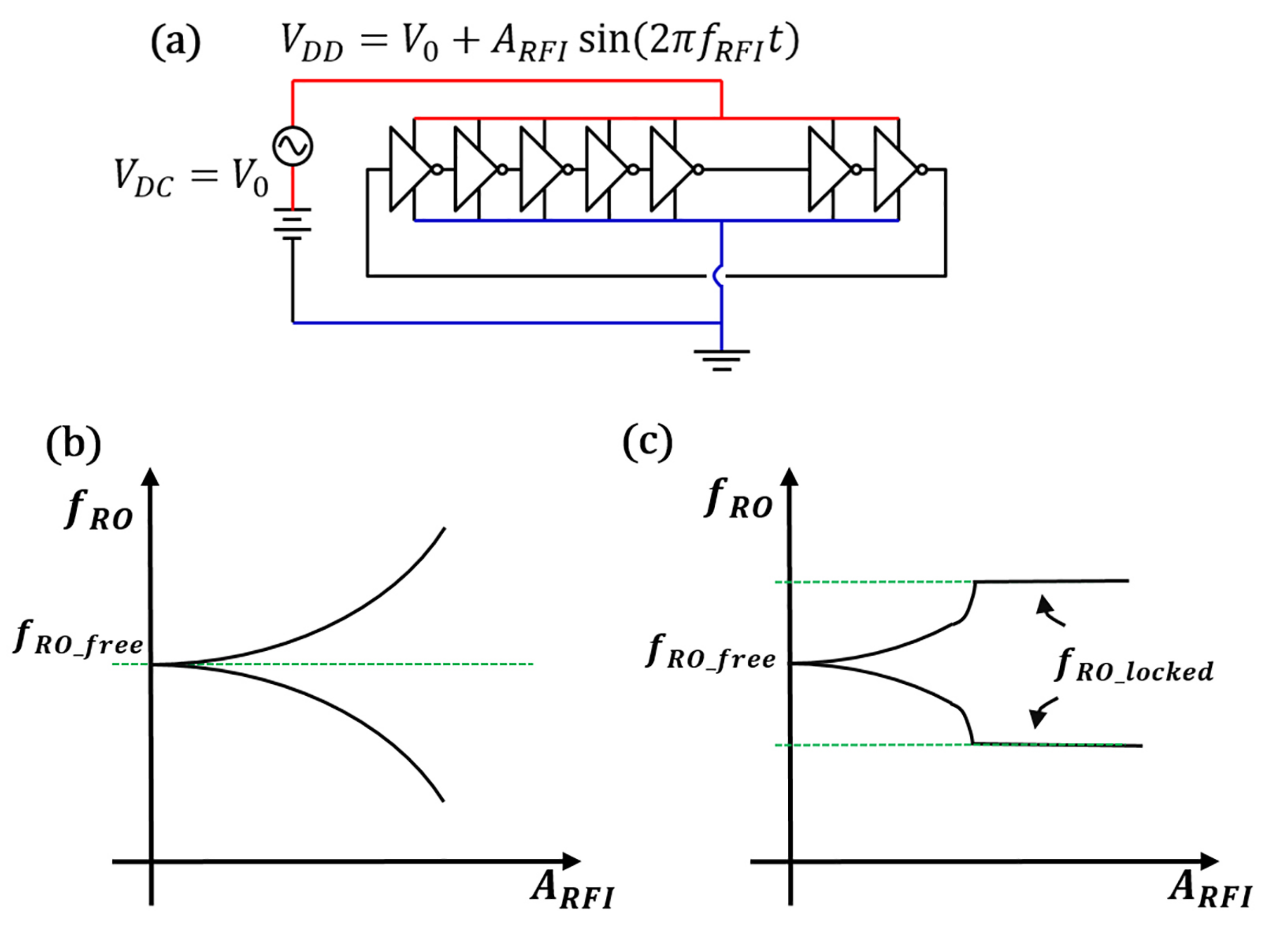
2. Injection Locking of Ring Oscillators
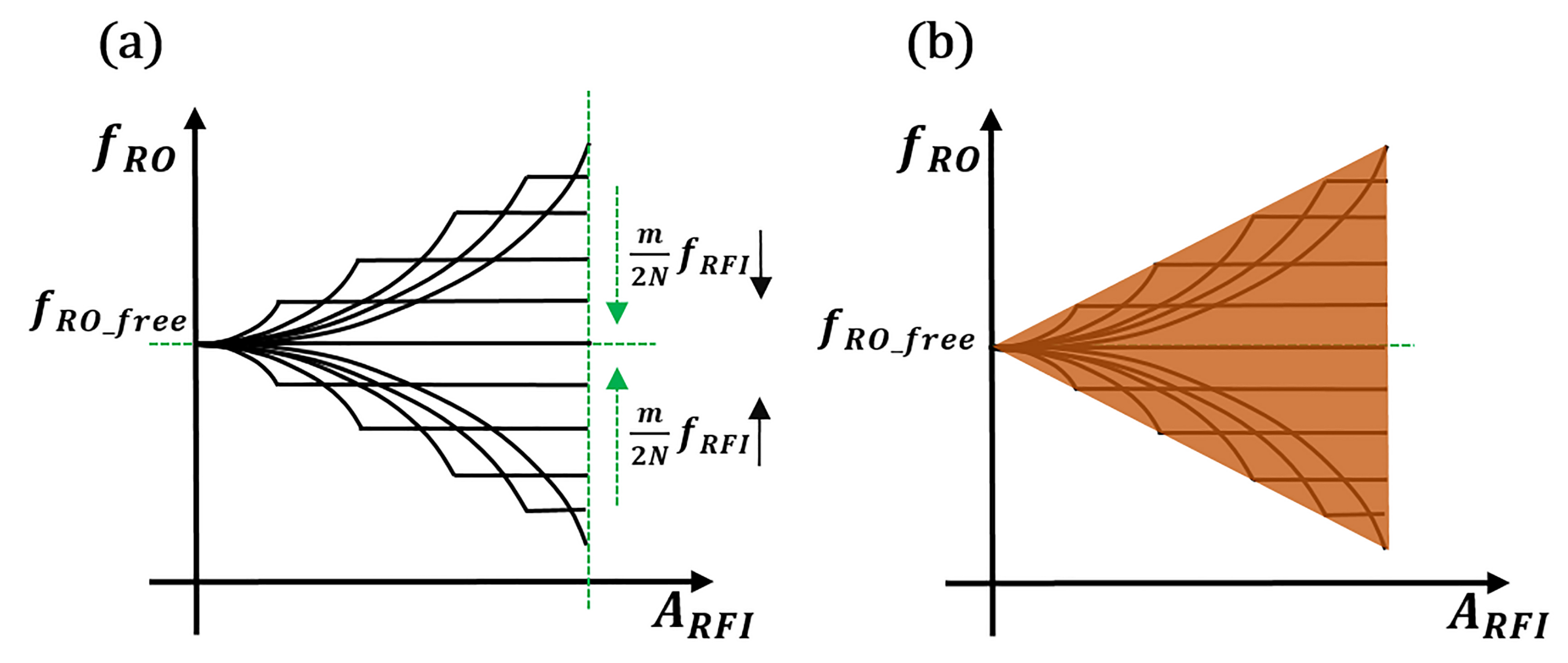
2.1. Conical Locking Region
2.2. Synchronous Locking of the Ring Oscillator Array
3. RO-Based TRNG Immunity Modeling and Optimization
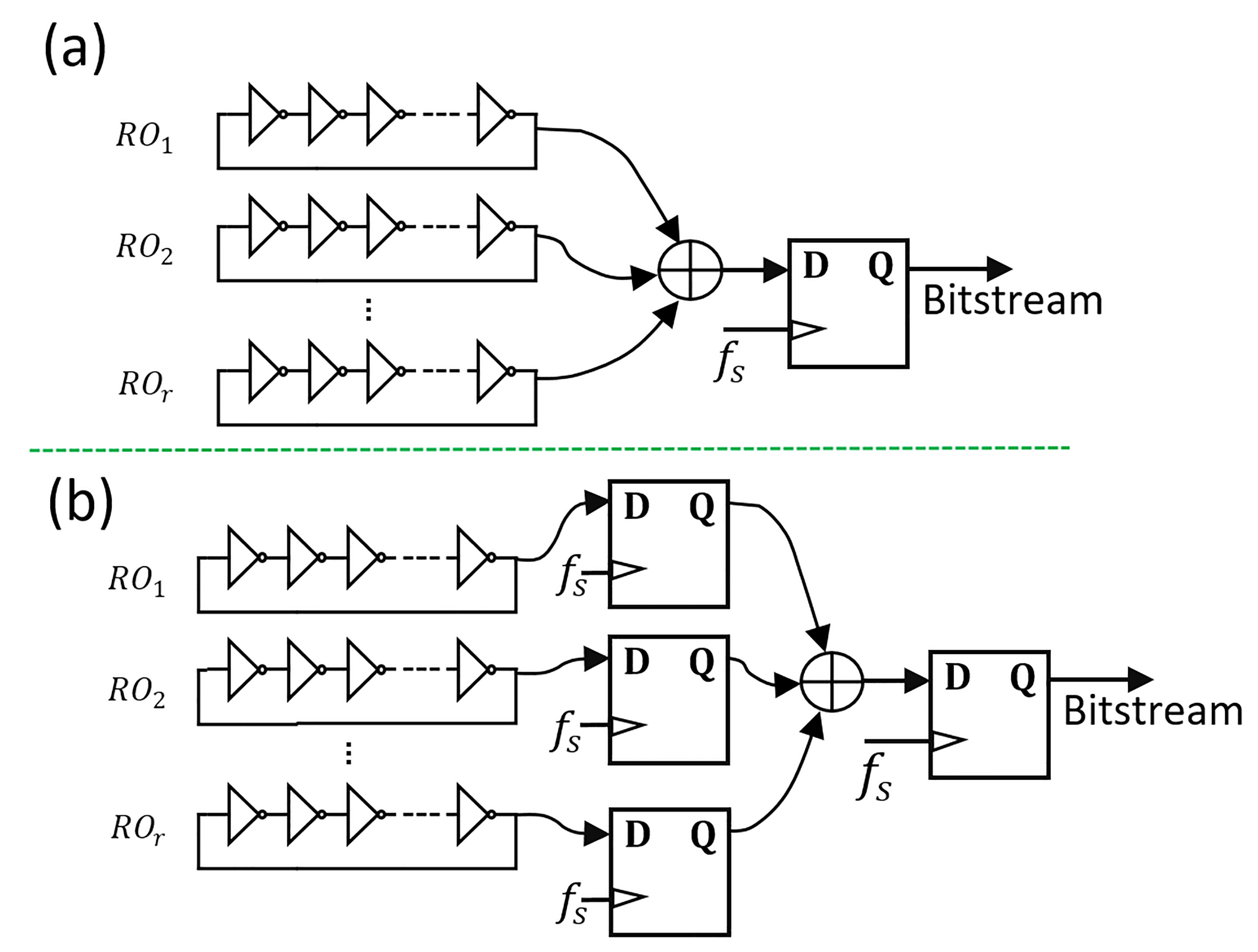
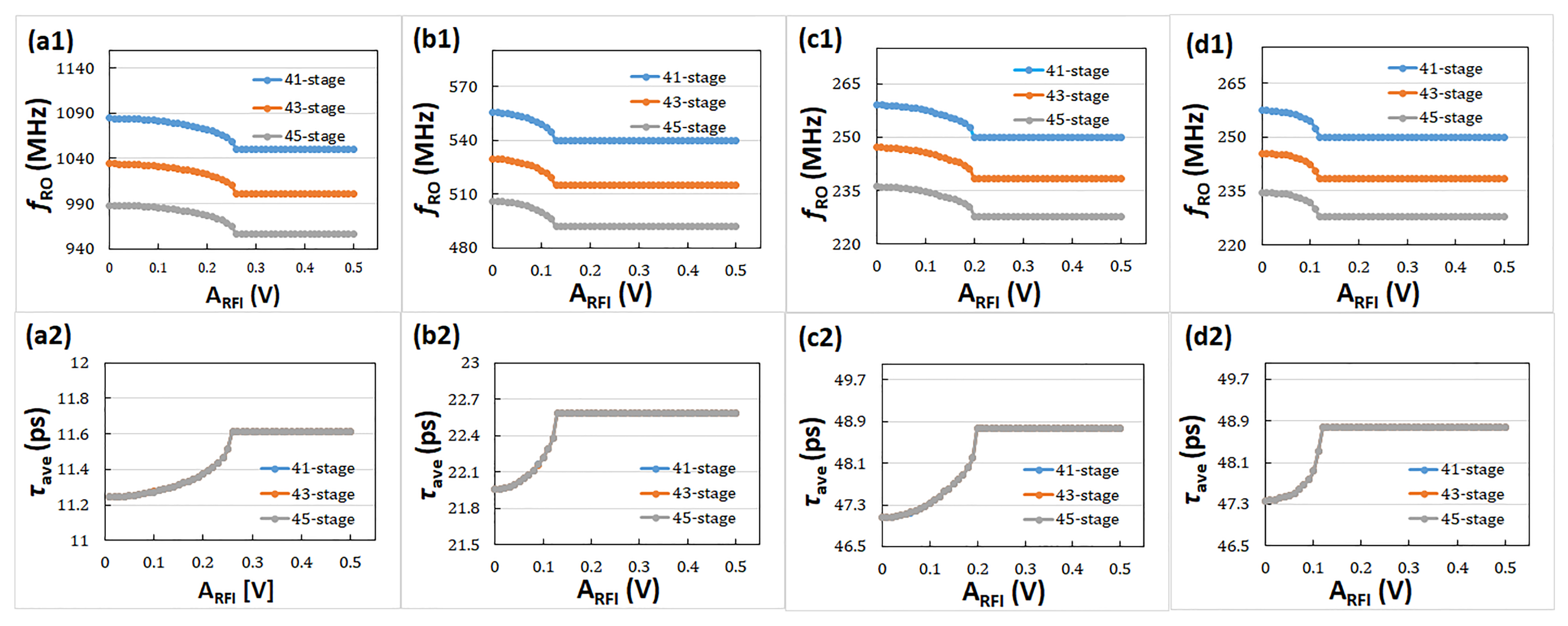
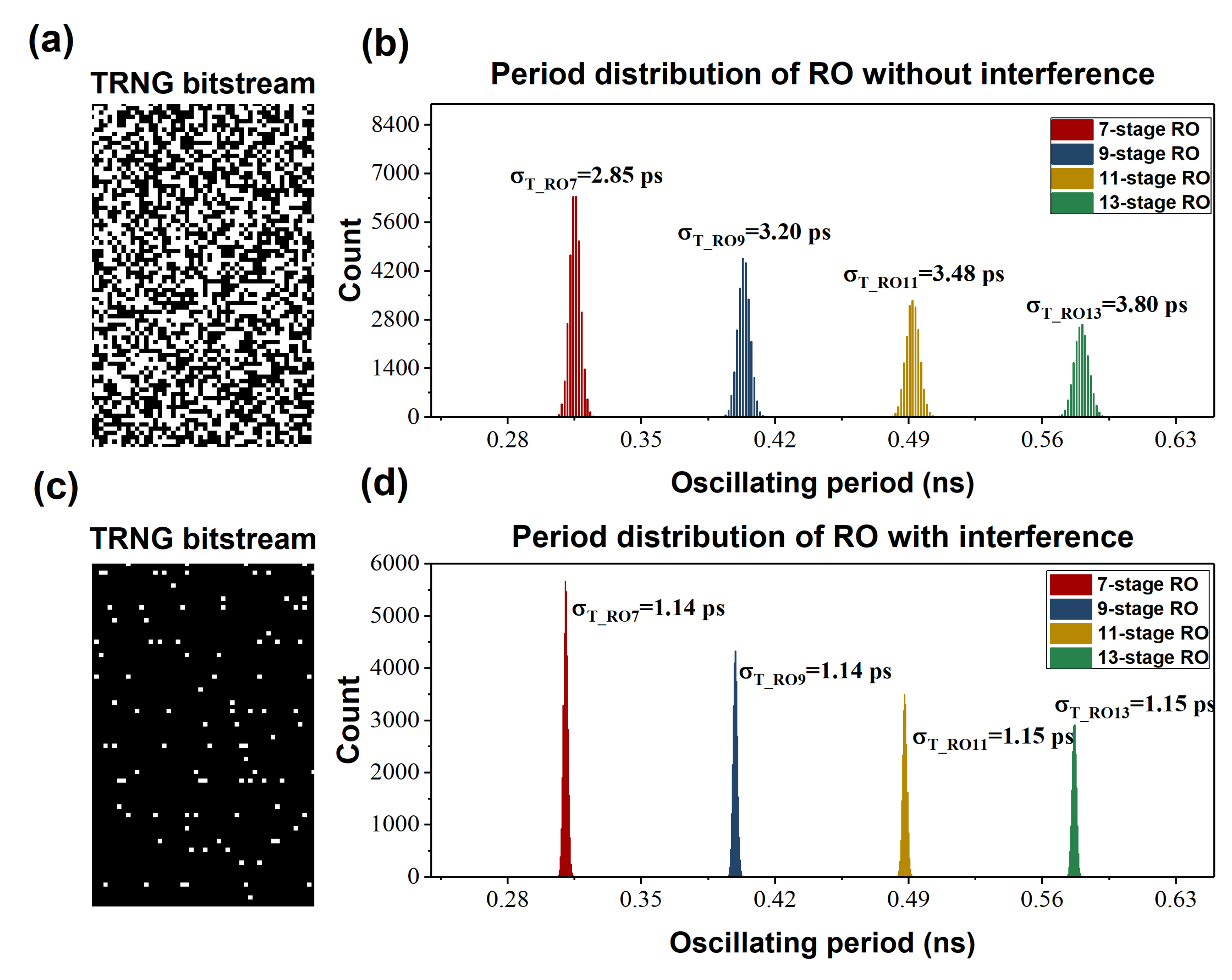
3.1. RO-Based TRNG Randomness-Degradation Mechanism
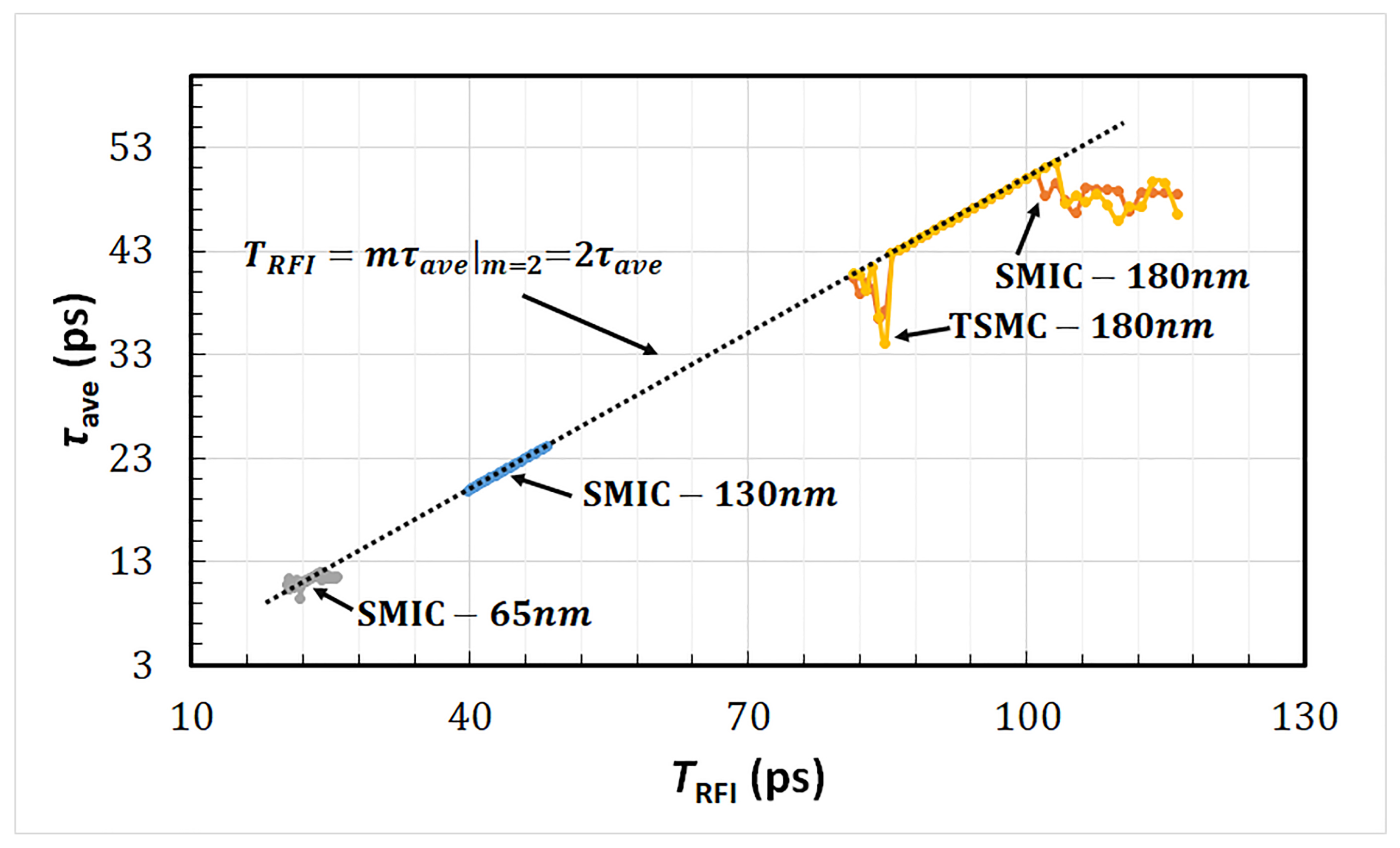
3.2. Immunity Modeling and Gate-Delay Differentiation
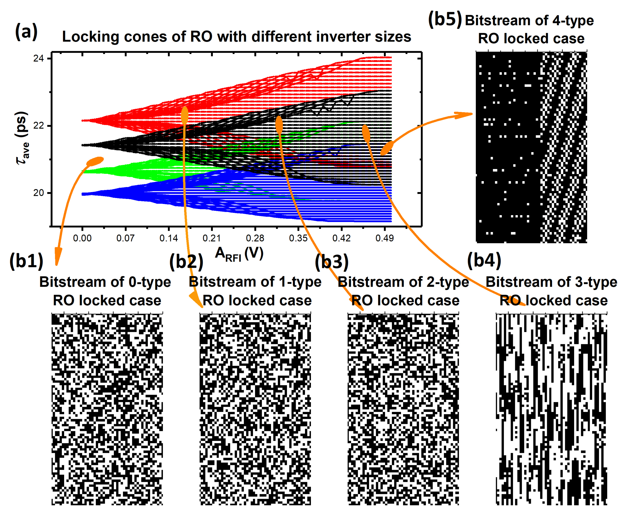
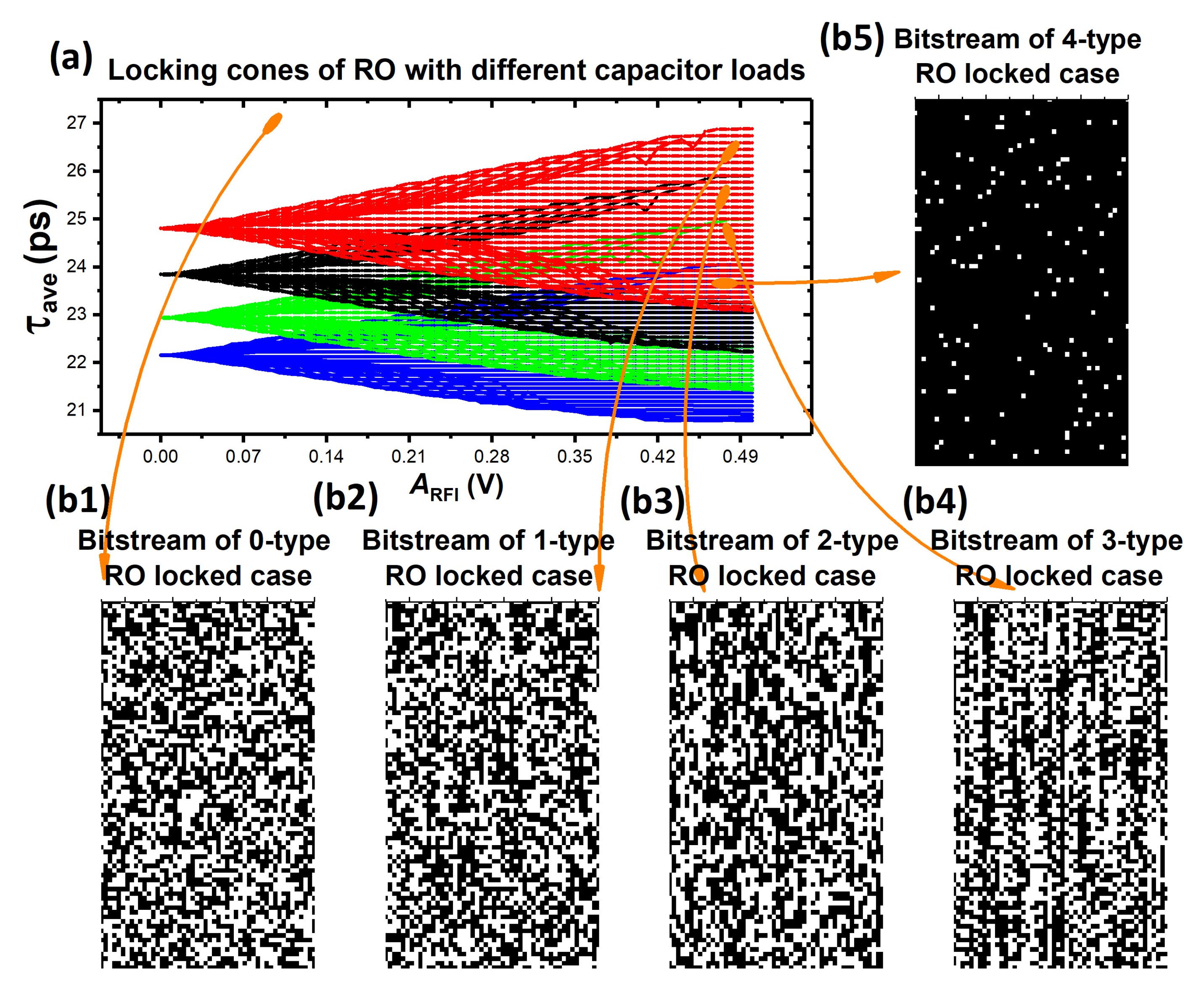
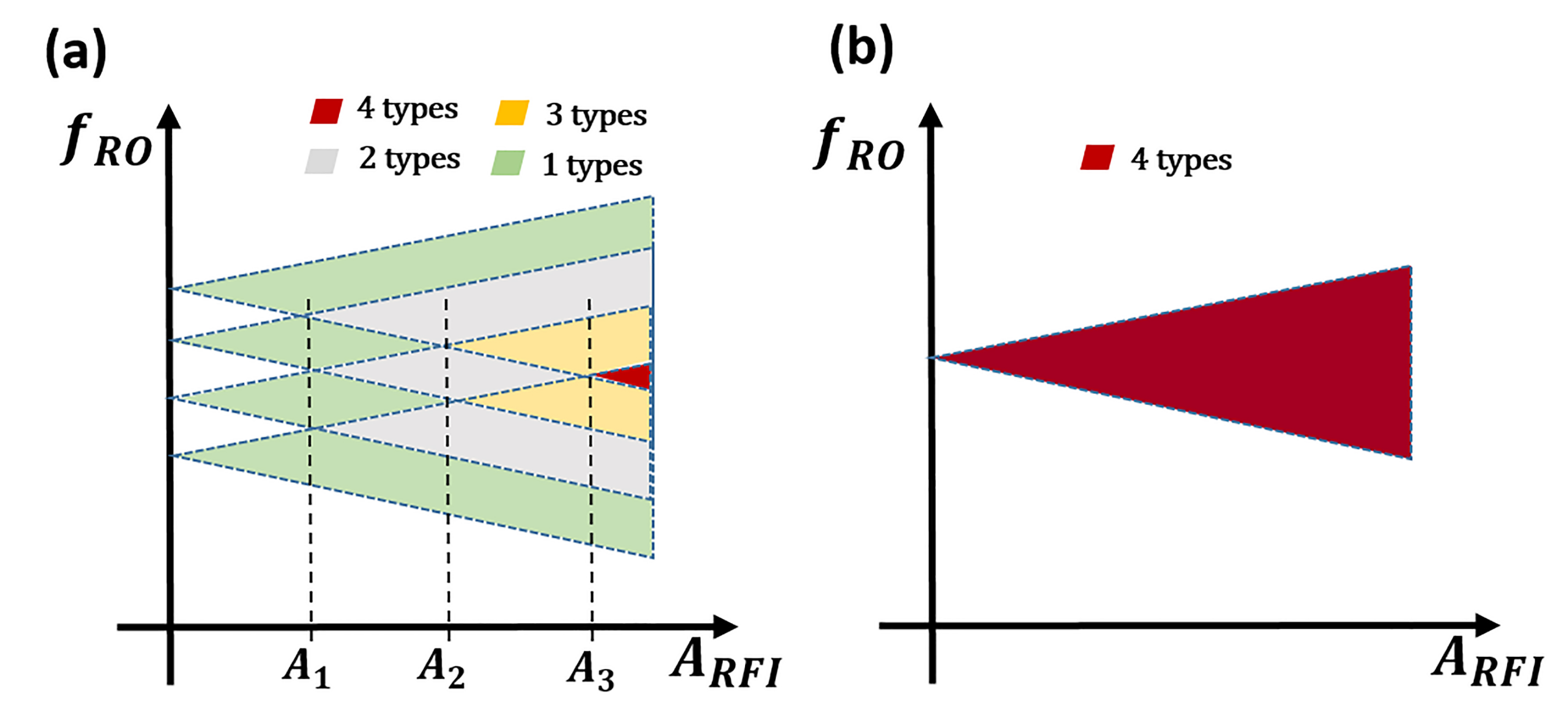
- To lock all four types of ROs, available and can only be selected in the red area, which is the overlapping area of the four conical locking regions. The required had to be greater than , and the selection of was also very harsh;
- To lock three types of ROs, the available and can only be selected in the yellow area. This required that > , and the available selection range of was also small;
- To lock two types of ROs, and can only be selected from the gray area. In such a case, it required > , and the selection range of was large. However, randomness did not become much worse because of only two types of ROs being locked;
- To lock one type of RO, and can only be selected from the light green area, which is easy to achieve. The influence of one type of RO locked on randomness can be ignored.
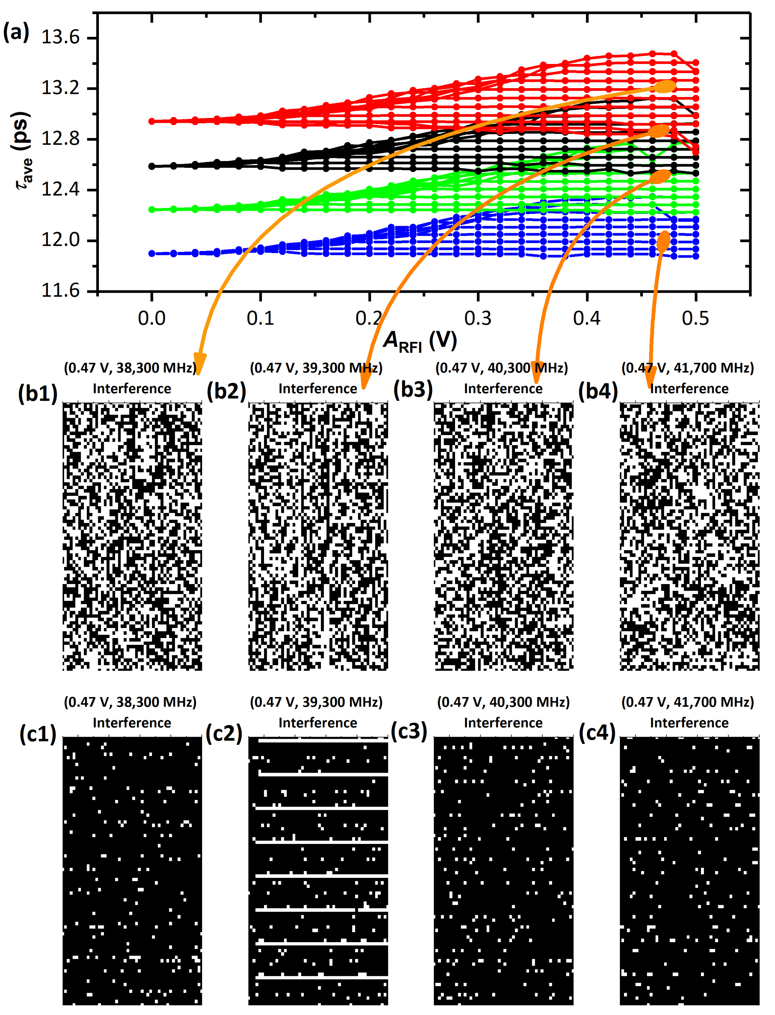
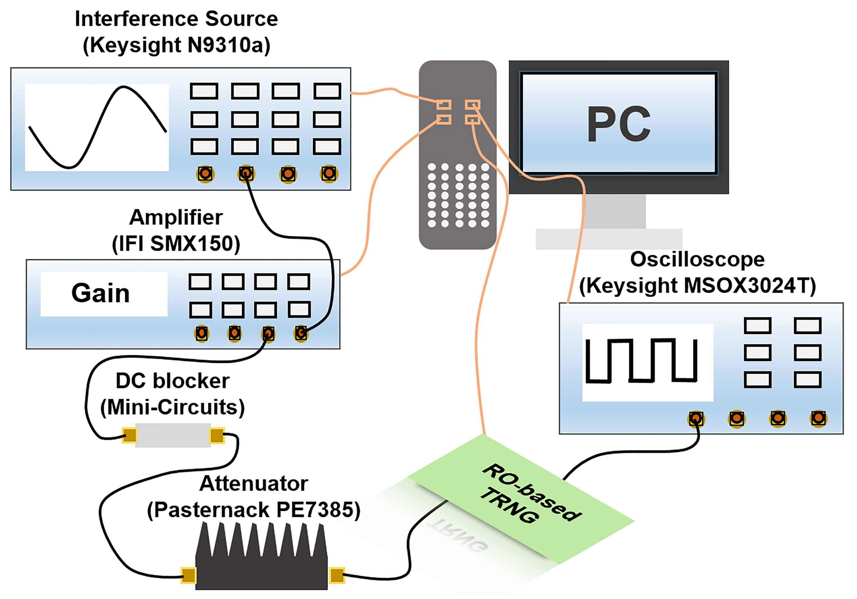
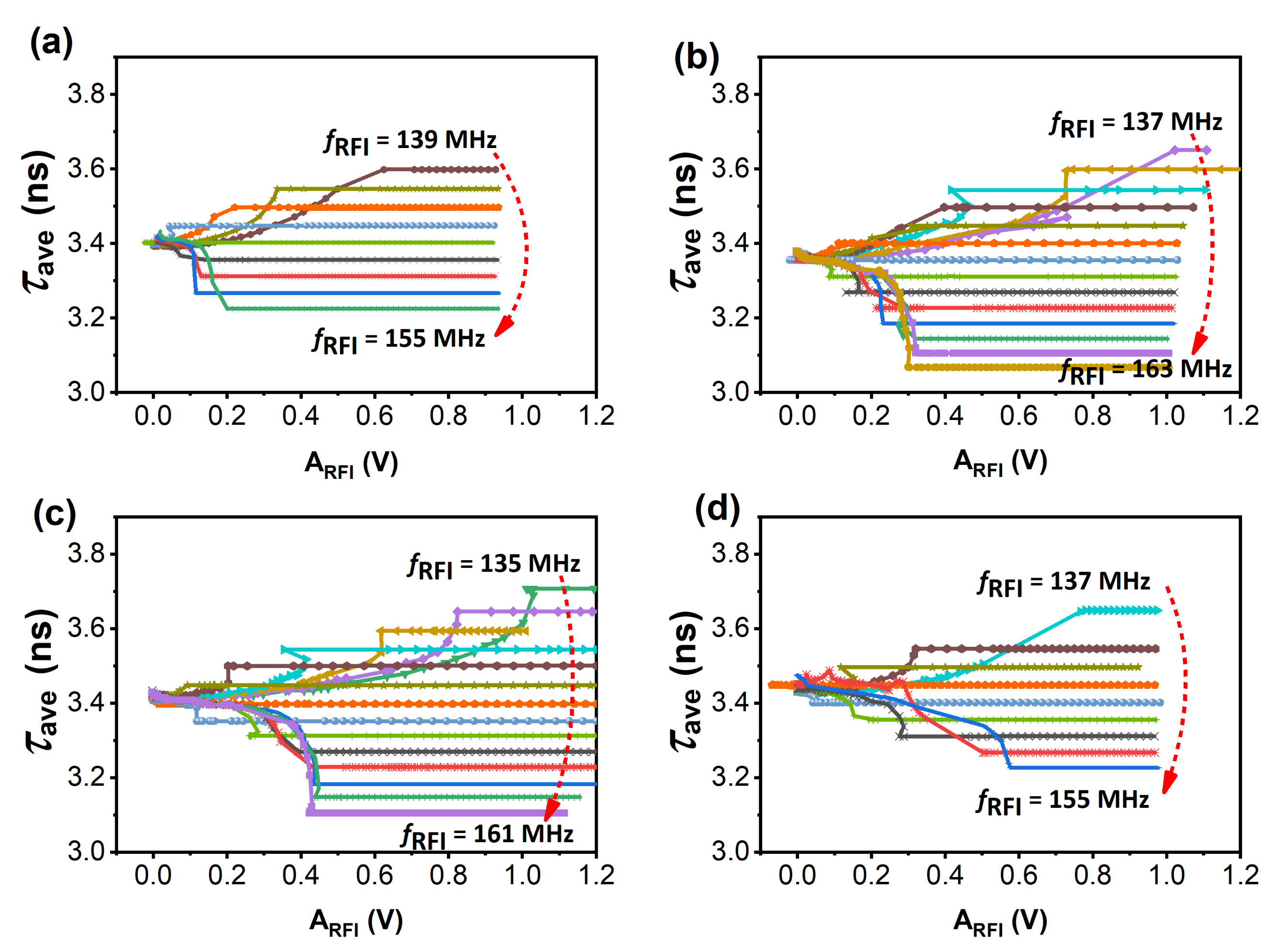
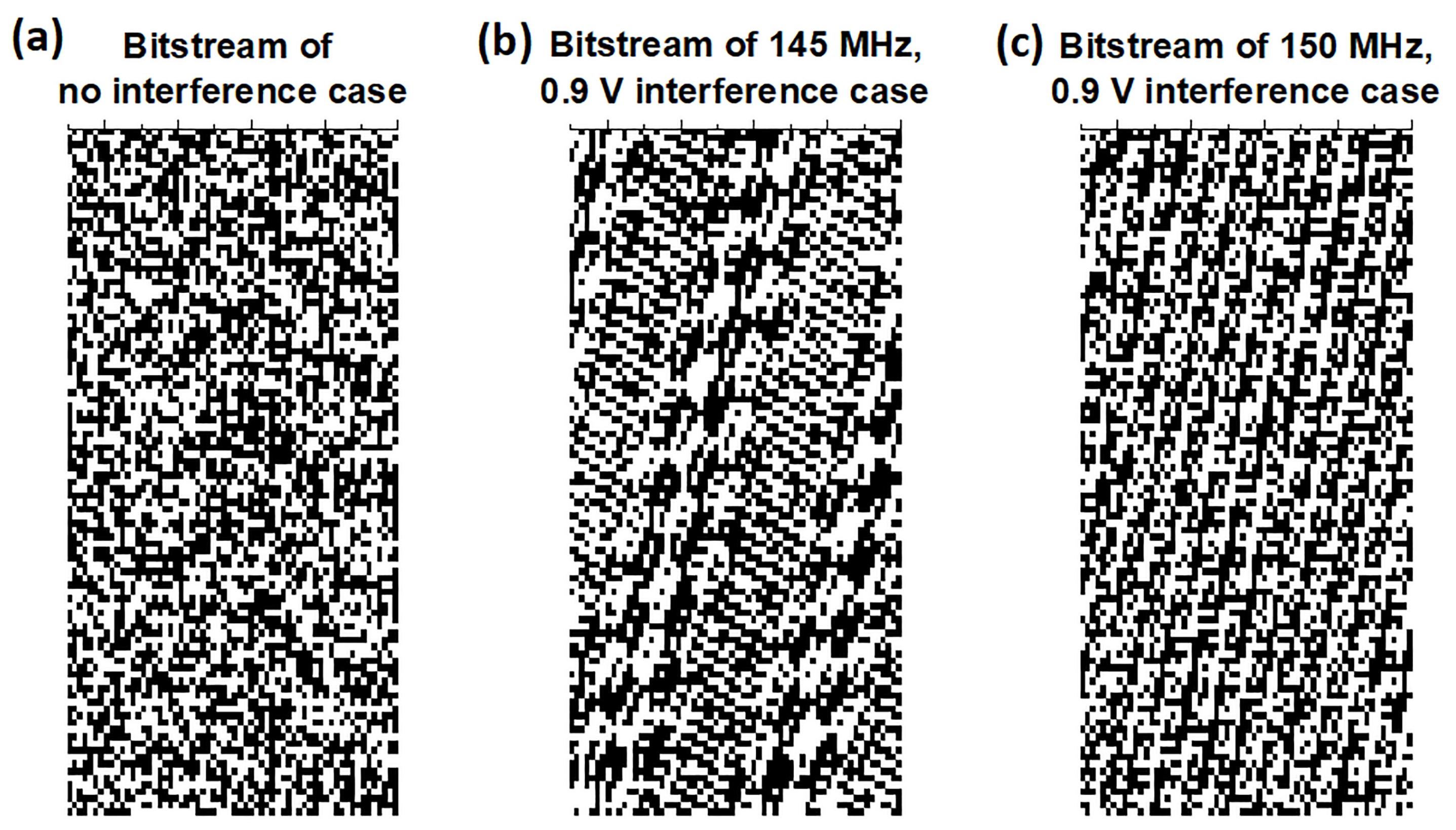
4. Measurement
5. Conclusions
Author Contributions
Funding
Conflicts of Interest
References
- Sunar, B.; Martin, W.J.; Stinson, D.R. A provably secure true random number generator with built-in tolerance to active attacks. IEEE Trans. Comput. 2007, 56, 109–119. [Google Scholar] [CrossRef]
- Wold, K.; Tan, C.H. Analysis and Enhancement of Random Number Generator in FPGA Based on Oscillator Rings. Int. J. Reconfigurable Comput. 2009, 2009, 4. [Google Scholar] [CrossRef] [Green Version]
- Rukhin, A.; Soto, J.; Nechvatal, J.; Smid, M.; Barker, E.; Leigh, S.; Levenson, M.; Vangel, M.; Banks, D.; Heckert, A.; et al. NIST Special Publication 800-22: A Statistical Test Suite for the Validation of Random Number Generators and Pseudo Random Number Generators for Cryptographic Applications; 2010 Technical Report; National Institute of Standards and Technology: Gaithersburg, MD, USA, 2010. [Google Scholar]
- Markettos, A.T.; Moore, S.W. The Frequency Injection Attack on Ring-Oscillator-Based True Random Number Generators. In Proceedings of the Cryptographic Hardware and Embedded Systems—Ches, Lausanne, Switzerland, 6–9 September 2009; Volume 5747, pp. 317–331. [Google Scholar]
- Bayon, P.; Bossuet, L.; Aubert, A.; Fischer, V.; Poucheret, F.; Robisson, B.; Maurine, P. Contactless Electromagnetic Active Attack on Ring Oscillator Based True Random Number Generator. In Proceedings of the International Workshop on Constructive Side-Channel Analysis and Secure Design, Darmstadt, Germany, 3–4 May 2012; Springer: Berlin/Heidelberg, Germany, 2012. [Google Scholar]
- Bayon, P.; Bossuet, L.; Aubert, A.; Fischer, V. Fault model of electromagnetic attacks targeting ring oscillator-based true random number generators. J. Cryptogr. Eng. 2016, 6, 61–74. [Google Scholar] [CrossRef] [Green Version]
- Osuka, S.; Fujimoto, D.; Hayashi, Y.; Homma, N.; Beckers, A.; Balasch, J.; Gierlichs, B.; Verbauwhede, I. EM Information Security Threats Against RO-Based TRNGs: The Frequency Injection Attack Based on IEMI and EM Information Leakage. IEEE Trans. Electromagn. Compat. 2019, 61, 1122–1128. [Google Scholar] [CrossRef]
- Schimmack, M.; Mercorelli, P. A structural property of the wavelet packet transform method to localise incoherency of a signal. J. Frankl. Inst. 2019, 356, 10123–10137. [Google Scholar] [CrossRef]
- Schimmack, M.; Mercorelli, P. An on-line orthogonal wavelet denoising algorithm for high-resolution surface scans. J. Frankl. Inst. 2018, 355, 9245–9270. [Google Scholar] [CrossRef]
- Ogasahara, Y.; Hashimoto, M.; Onoye, T. All-Digital Ring-Oscillator-Based Macro for Sensing Dynamic Supply Noise Waveform. IEEE J. Solid State Circuits 2009, 44, 1745–1755. [Google Scholar] [CrossRef] [Green Version]
- An, Y.J.; Jung, D.H.; Ryu, K.; Yim, H.S.; Jung, S.O. All-Digital ON-Chip Process Sensor Using Ratioed Inverter-Based Ring Oscillator. IEEE Trans. Very Large Scale Integr. (VLSI) Syst. 2016, 24, 3232–3242. [Google Scholar] [CrossRef]
- Hong, B.; Hajimiri, A. A Phasor-Based Analysis of Sinusoidal Injection Locking in LC and Ring Oscillators. IEEE Trans. Circuits Syst. I Regul. Pap. 2019, 66, 355–368. [Google Scholar] [CrossRef]
- Liu, S.; Zheng, Y.; Lim, W.M.; Yang, W. Ring Oscillator Based Injection Locked Frequency Divider Using Dual Injection Paths. IEEE Microw. Wirel. Compon. Lett. 2015, 25, 322–324. [Google Scholar] [CrossRef]
- Mirzaei, A.; Heidari, M.E.; Bagheri, R.; Abidi, A.A. Multi-Phase Injection Widens Lock Range of Ring-Oscillator-Based Frequency Dividers. IEEE J. Solid State Circuits 2008, 43, 656–671. [Google Scholar] [CrossRef]
- Razavi, B. A study of injection locking and pulling in oscillators. IEEE J. Solid State Circuits 2004, 39, 1415–1424. [Google Scholar] [CrossRef]
- Mureddu, U.; Bochard, N.; Bossuet, L.; Fischer, V. Experimental Study of Locking Phenomena on Oscillating Rings Implemented in Logic Devices. IEEE Trans. Circuits Syst. I Regul. Pap. 2019, 66, 2560–2571. [Google Scholar] [CrossRef]
- Su, T.; Li, F.; Lian, Z.; Feng, Z.; Li, Y.; Liu, Z. Frequency Shift of Ring Oscillators Due to Radio Frequency Interference on the Supply. IEEE Trans. Electromagn. Compat. 2015, 57, 1365–1373. [Google Scholar] [CrossRef]
- Xiao, Z.; Chen, D.; Su, T. Locking of RO due to RF interference in supply. Electron. Lett. 2019, 55, 254–256. [Google Scholar] [CrossRef]


| SMIC-65 nm | SMIC-130 nm | |||||
|---|---|---|---|---|---|---|
| 41-Stage | 43-Stage | 45-Stage | 41-Stage | 43-Stage | 45-Stage | |
| (MHz) | 1050 | 1001 | 957 | 540 | 515 | 492 |
| (ps) | 11.61 | 11.61 | 11.61 | 22.58 | 22.58 | 22.58 |
| SMIC-180 nm | TSMC-180 nm | |||||
| 41-Stage | 43-Stage | 45-Stage | 41-Stage | 43-Stage | 45-Stage | |
| (MHz) | 250 | 238 | 228 | 250 | 238 | 228 |
| (ps) | 48.78 | 48.78 | 48.78 | 48.78 | 48.78 | 48.78 |
| 7-Stage RO | 9-Stage RO | 11-Stage RO | 13-Stage RO | |
|---|---|---|---|---|
| 3166 MHz | 2476 MHz | 2034 MHz | 1726 MHz | |
| 22.56 ps | 22.44 ps | 22.35 ps | 22.29 ps | |
| Jitter without EMI | 2.85 ps | 3.20 ps | 3.48 ps | 3.80 ps |
| Jitter with EMI | 1.14 ps | 1.14 ps | 1.15 ps | 1.15 ps |
| Percentage of suppressed jitter | 60% | 64% | 67% | 70% |
| 7-Stage RO | 9-Stage RO | 11-Stage RO | 13-Stage RO | |
|---|---|---|---|---|
| Case 1 | = 0.40 μ; | = 0.98 μ; | = 2.22 μ; | = 7.70 μ; |
| = 0.61 μ | = 1.49 μ | = 3.38 μ | = 11.74 μ | |
| Case 2 | = 0 fF | = 0.13 fF | = 0.28 fF | = 0.44 fF |
| Jitters of ROs (ps) | ||||
|---|---|---|---|---|
| (V, MHz) | 7-Stage | 9-Stage | 11-Stage | 13-Stage |
| 23,700 | 3.37 | 3.92 | 4.08 | 3.69 |
| 22,500 | 1.90 | 5.73 | 5.07 | 4.16 |
| 22,800 | 1.27 | 1.31 | 9.16 | 5.60 |
| 23,100 | 0.92 | 0.87 | 1.01 | 9.05 |
| 23,370 | 0.90 | 0.81 | 0.85 | 1.51 |
| Jitters of ROs (ps) | ||||
|---|---|---|---|---|
| (V, MHz) | 7-Stage | 9-Stage | 11-Stage | 13-Stage |
| 18,050 | 3.70 | 4.67 | 4.75 | 4.81 |
| 18,868 | 10.89 | 13.20 | 14.77 | 1.17 |
| 19,455 | 13.49 | 13.63 | 1.20 | 1.00 |
| 20,080 | 10.62 | 1.20 | 0.99 | 0.94 |
| 20,408 | 1.32 | 1.06 | 0.96 | 0.92 |
| 7-Stage RO | 9-Stage RO | 11-Stage RO | 13-Stage RO |
|---|---|---|---|
| = 0 fF | = 0.13 fF | = 0.28 fF | = 0.44 fF |
Publisher’s Note: MDPI stays neutral with regard to jurisdictional claims in published maps and institutional affiliations. |
© 2021 by the authors. Licensee MDPI, Basel, Switzerland. This article is an open access article distributed under the terms and conditions of the Creative Commons Attribution (CC BY) license (https://creativecommons.org/licenses/by/4.0/).
Share and Cite
Zhang, Z.; Su, T. Behavioral Analysis and Immunity Design of the RO-Based TRNG under Electromagnetic Interference. Electronics 2021, 10, 1347. https://doi.org/10.3390/electronics10111347
Zhang Z, Su T. Behavioral Analysis and Immunity Design of the RO-Based TRNG under Electromagnetic Interference. Electronics. 2021; 10(11):1347. https://doi.org/10.3390/electronics10111347
Chicago/Turabian StyleZhang, Zhiwen, and Tao Su. 2021. "Behavioral Analysis and Immunity Design of the RO-Based TRNG under Electromagnetic Interference" Electronics 10, no. 11: 1347. https://doi.org/10.3390/electronics10111347
APA StyleZhang, Z., & Su, T. (2021). Behavioral Analysis and Immunity Design of the RO-Based TRNG under Electromagnetic Interference. Electronics, 10(11), 1347. https://doi.org/10.3390/electronics10111347