Article

Ring-Oscillator with Multiple Transconductors for Linear Analog-to-Digital Conversion

1
Electronics Technology Department, Carlos III University, 28903 Madrid, Spain
2
MaxLinear Austria, 9524 Villach, Austria
3
Thomas Johann Seebeck Department of Electronics, Tallinn University of Technology, 12616 Tallinn, Estonia
*
Author to whom correspondence should be addressed.
These authors contributed equally to this work.
Electronics 2021, 10(12), 1408; https://doi.org/10.3390/electronics10121408
Submission received: 29 April 2021 / Revised: 8 June 2021 / Accepted: 10 June 2021 / Published: 11 June 2021
(This article belongs to the Special Issue Low Power Circuits in Microelectronics)

Abstract

:
This paper proposes a new circuit-based approach to mitigate nonlinearity in open-loop ring-oscillator-based analog-to-digital converters (ADCs). The approach consists of driving a current-controlled oscillator (CCO) with several transconductors connected in parallel with different bias conditions. The current injected into the oscillator can then be properly sized to linearize the oscillator, performing the inverse current-to-frequency function. To evaluate the approach, a circuit example has been designed in a 65-nm CMOS process, leading to a more than 3-ENOB enhancement in simulation for a high-swing differential input voltage signal of 800-mV pp , with considerable less complex design and lower power and expected area in comparison to state-of-the-art circuit based solutions. The architecture has also been checked against PVT and mismatch variations, proving to be highly robust, requiring only very simple calibration techniques. The solution is especially suitable for high-bandwidth (tens of MHz) medium-resolution applications (10–12 ENOBs), such as 5G or Internet-of-Things (IoT) devices.

1. Introduction

The scaling down of CMOS processes has posed new challenges for analog-to-digital conversion, especially from the analog design perspective. Digital logic consumes less power, occupies less area, and works faster as design processes get smaller. Nevertheless, analog designs have become highly complex due to the low voltage supply and limited devices’ gain, higher noise impact, mismatch, and parasitic effects [1]. Thus, the current trend is towards mostly digital implementations.
Energy-efficient wide-band ADCs are essential for applications such as portable battery-powered devices or radio-receivers. Flash ADCs are usually implemented for high-speed analog-to-digital conversion [2]. However, the power consumption increases exponentially with the number of bits, making them less power-efficient for more than 10 ENOBs [3]. Additionally, they are extremely sensitive to mismatch phenomena when implemented with minimum-size devices and not scalable. To minimize this impact, devices’ dimensions are often increased at the cost of larger occupied area and higher power consumption [4,5].
SAR (Successive Approximation Register) ADCs are low-power, simple, and friendly-digital architectures. They are more energy-efficient than Flash-based architectures due to their mostly-digital implementation suitable with modern processes nodes [6,7]. Nevertheless, their sampling rate is limited by the need of a high-speed clock for the control logic [2], limiting their use for medium bandwidth and leading to dramatically high-power solutions when used for MHz-bandwidths [8,9,10,11].
Pipeline ADCs divide the analog-to-digital high-resolution conversion operation into several low-resolution conversion stages operating sequentially, showing a proper balance between accuracy and operation speed. The drawback of this kind of ADCs is the high-performance operational amplifier (opamp) mandated by a multiplyng digital-to-analog converter (MDAC) [2]. This block consumes a large amount of power, reducing the power efficiency, and entails challenging designs in deep submicron CMOS nodes [12,13].
Time-interleaved (TI) architectures combine low-speed ADCs connected in parallel and sampled with uniformly distributed different phases from a single clock signal to achieve a high sampling rate and high energy efficiency [2]. SAR, Flash, and pipeline ADCs are commonly used in TI-based structures. However, mismatch phenomena among the channels significantly degrade the resolution. To alleviate this issue, calibration circuits are needed, which require extra power consumption and increase the system complexity [14,15].
Continuous-Time Delta-Sigma ( Δ Σ ) modulator (CTSDM) ADCs have also been reported for wide-band analog-to-digital conversion [16], but some key points such as the analog nature of the filter loop, the excess loop delay, and the clock jitter increase the complexity design especially with narrow processes nodes. Noise-Shaping SAR (NS-SAR) structures combined with time-interleaving techniques remove the need for analog-circuits, relaxing technology scaling requirements and enabling high-bandwidth conversion with lower power consumption [17,18].
Voltage-controlled oscillator based analog-to-digital converters (VCO-based ADCs) have emerged as a promising solution due to their highly digital nature adequate for very low voltage supplies. Diverse hybrid structures with VCOs have been published: with VCOs as integrators/quantizers in CTSDMs [19,20,21,22,23], placing it into SAR-based structures for pipeline ADCs [24,25,26,27] or in multi-stage noise shaping (MASH) architectures [28,29,30,31]. If we look for simplicity, they are of special interest if a ring-oscillator is used in an open-loop configuration [32,33,34]. Apart from its simple digital architecture, composed of CMOS logic gates (NOT gates), the spectral properties of pulse frequency modulation enable first-order noise-shaped output data, with a performance similar to CTSDMs [35].
The main limitation of the ring-oscillator is the nonlinear voltage/current-to-frequency response, which translates into distortion and limits the dynamic range of the whole ADC. Several ways of correcting the ring-oscillators’ nonlinearity have been proposed in the literature. One of the most explored is digital calibration that requires large occupied area and wastes a lot of power [32,36]. Circuit-level solutions have also been introduced at the cost of a much lower oscillator gain [37] or more complex designs [38], being in many cases in applications for low-bandwidth ADCs. Another alternative consists of a VCO-based quantizer within a CTSDM [19,22], where the nonlinearity is corrected by the gain of the loop at the expense of more complex and non-scalable structures.
In this work, we propose a new way to mitigate the distortion generated by the nonlinearity of the ring-oscillator, exploiting a circuit design with significantly lower power consumption and area comparing to prior art. The idea makes use of several transconductors with different bias conditions connected in parallel to inject the current into a current-controlled oscillator (CCO) architecture. By means of selecting a proper distribution of those bias conditions, we can implement a nonlinear voltage-to-current function that approximates the inverse nonlinear current-to-frequency CCO relation. Figure 1 depicts a scheme that summarizes the idea described above. The VCO is composed of an input stage that converts an input voltage into a current, and a CCO that makes a current-to-frequency translation (Figure 1a). The transfer functions of both the front-end circuit and the ring-oscillator affect the whole response of the VCO (Figure 1b). To compensate for the nonlinearity of the structure, the inverse nonlinear function of the oscillator is artificially performed by the front-end circuit, thus canceling both nonlinear effects (Figure 1c). Something similar was already proposed in [39] with a resistive divider as the oscillator front-end circuit. The main disadvantage is that the input signal attenuation directly entails a lower dynamic range.
The possibility of going towards a fully-synthesizable architecture might be considered in the future, but it is currently out of the scope of the present manuscript, mainly due to the analog nature of the transconductors. All the digital parts can be implemented by using digital synthesis [3,6,7,40,41,42,43,44,45]. Tools for automated analog design are on-the-spot now and may become of application for the current architecture [46,47,48,49].
Our proposal is evaluated by transient simulation with a low power (LP) TSMC 65-nm CMOS process, showing excellent performance in power and area, especially compared to digital calibration techniques [32], significantly reducing the total harmonic distortion (THD) power. In addition, PVT variation and Monte Carlo simulations show that the solution is robust against those variations, requiring simple calibration to achieve substantial distortion enhancement and proper resolution improvement for high-swing input signals. Finally, the proposed circuit is completely scalable as the calibration is also performed digitally, making it suitable for PVT/mismatch compensation in very deep submicron CMOS nodes such as 16-nm or 7-nm.

2. Materials and Methods

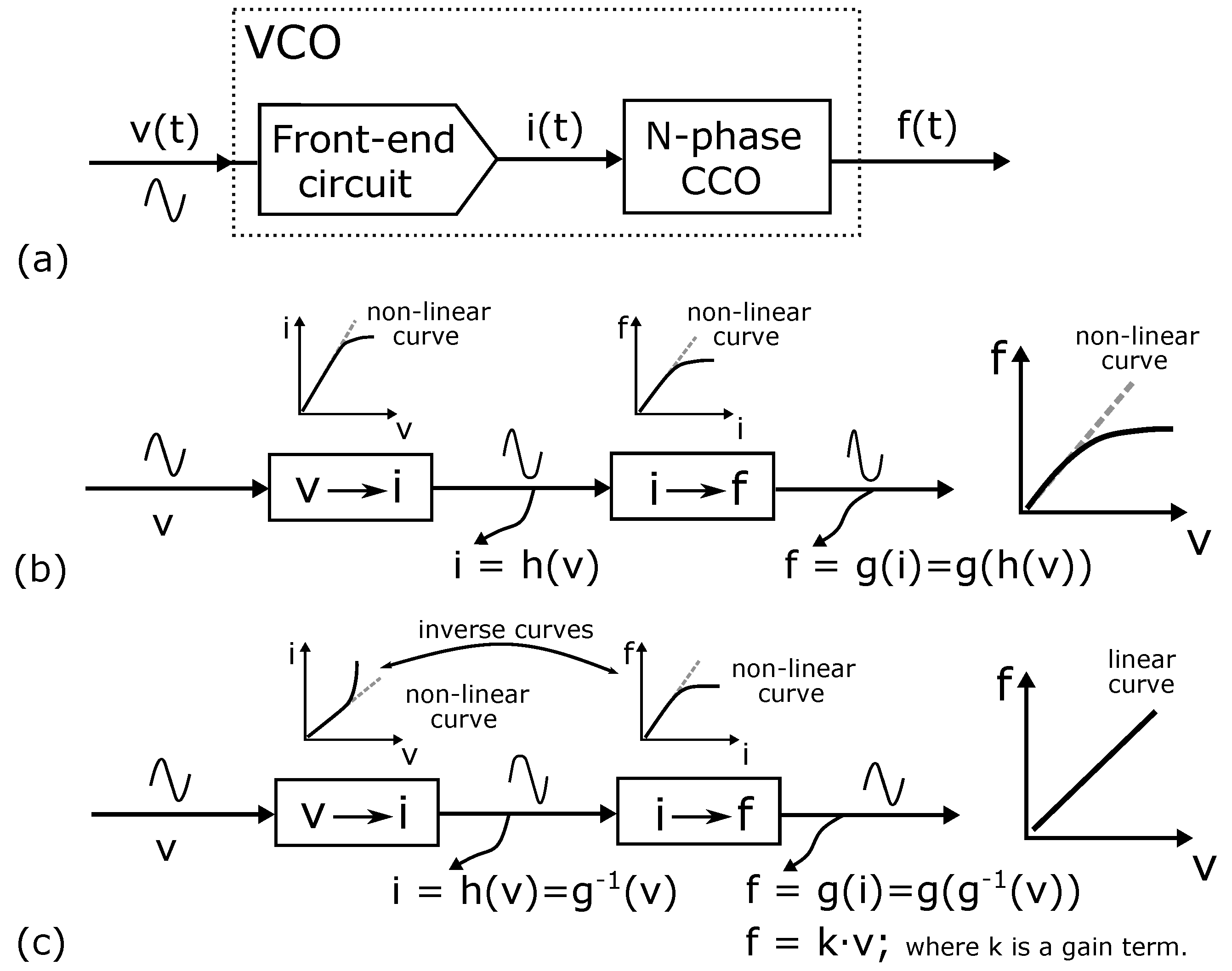
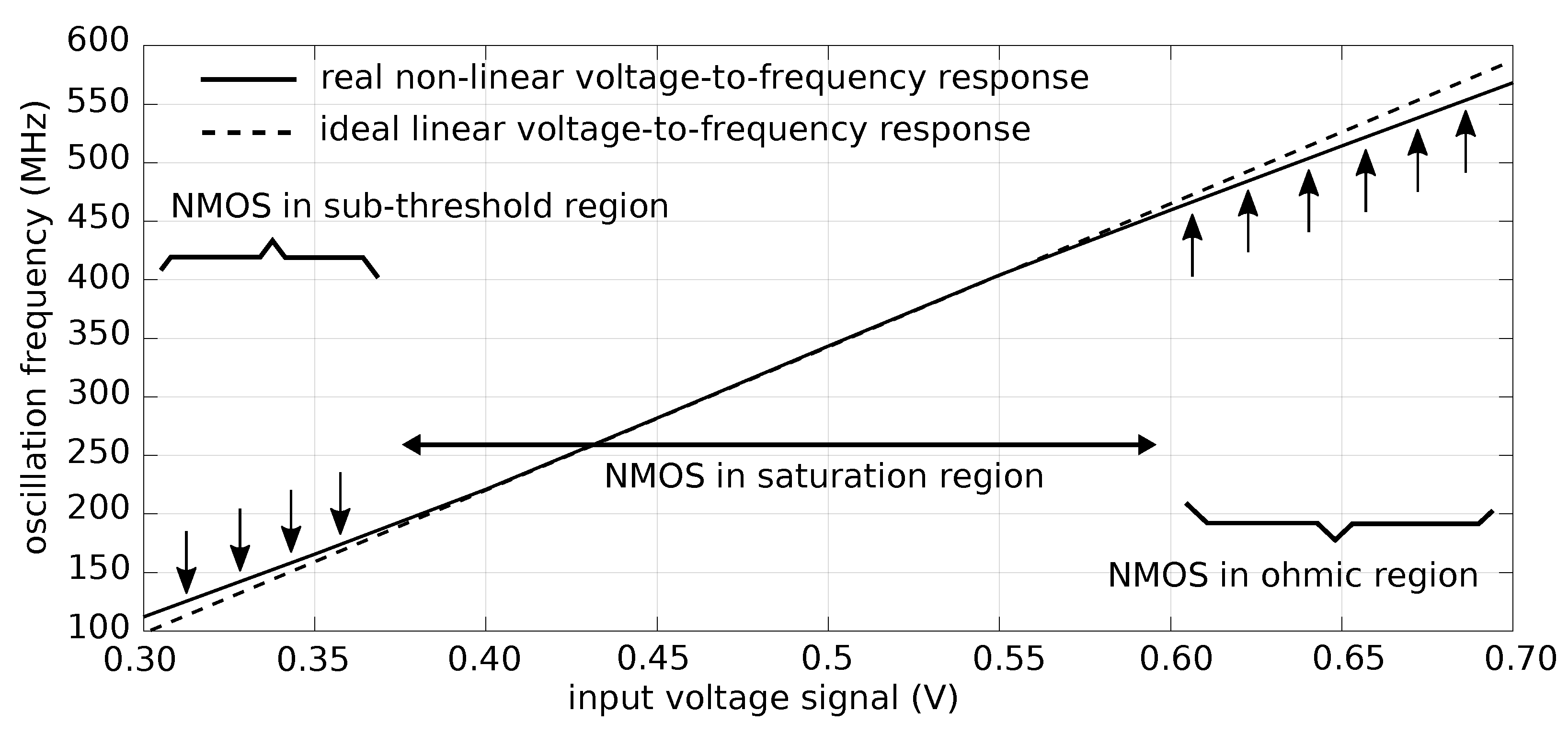
2.1. Nonlinearity in Ring-Oscillators

The conventional structure for a pseudo-differential open-loop VCO-based ADC is depicted in Figure 2a, built with one ring-oscillator per branch followed by some digital logic that samples and computes the first difference of the output phases (Figure 2b [35]). The VCO is composed of a transconductor-based front-end stage (g m ) and an N-phase CCO. The voltage-to-current conversion could be performed with a single NMOS transistor. Here, the instantaneous oscillation frequency ( f osc ( t ) ) of the ring-oscillator follows the expression:
f osc ( t ) = f o + K VCO · g m · x ( t ) ,
where f o is the rest oscillation frequency, K VCO is the ring-oscillator gain, g m is the transconductance of the front-end circuit (the single NMOS device in Figure 2b), and x ( t ) is the input voltage centered at zero. Level shifters are required to saturate amplitude-modulated oscillator output signals before being sampled and operated in discrete time.
As open-loop configuration corresponds to a highly technology-scalable architecture; this ring-oscillator is implemented with conventional CMOS logic gates and the circuitry afterward is composed of registers and XOR gates. However, the voltage-to-frequency response of the VCO is not linear due to the nonlinear time-delay dependence of the logic gates of the oscillator with respect to the flowing current [50], and the nonlinear voltage-to-current relation in the transconductance g m .
To have some intuition about the ring-oscillator nonlinear characteristic and its effect on the output data, a behavioral model of Figure 2 was designed in a 65-nm CMOS technology. The model included a 45-phase ring-oscillator with the rest of the blocks modeled with Verilog-A. The sampling frequency ( f s ) was 2 GHz with an analog bandwidth (ABW) of 50 MHz. The oscillation parameters were f o = 450 MHz and K VCO · g m = 1 GHz/V, for a 3 MHz sinusoidal differential input signal of 800 mV pp . The nominal voltage supply was 1.2 V.
Figure 3 depicts the spectrum of the output data y [ n ] resulting from a transient simulation. The harmonic distortion is clearly visible, with the third and fifth harmonic distortion terms (HD3 and HD5) equal to −44 dBc and −68 dBc, respectively (the second harmonic distortion term, HD2, term was −39 dBc in a single-ended configuration). The signal-to-noise ratio (SNR) is 63 dB and the signal-to-noise-distortion ratio (SNDR) is 44 dB, which means a degradation of approximately three ENOBs due to distortion. As seen, a peak SNDR higher than 50 dB becomes impossible, making this architecture unsuitable for next generation WLAN standard or 5G, where a peak SNDR higher than 65 dB over wide bandwidth is required [51].

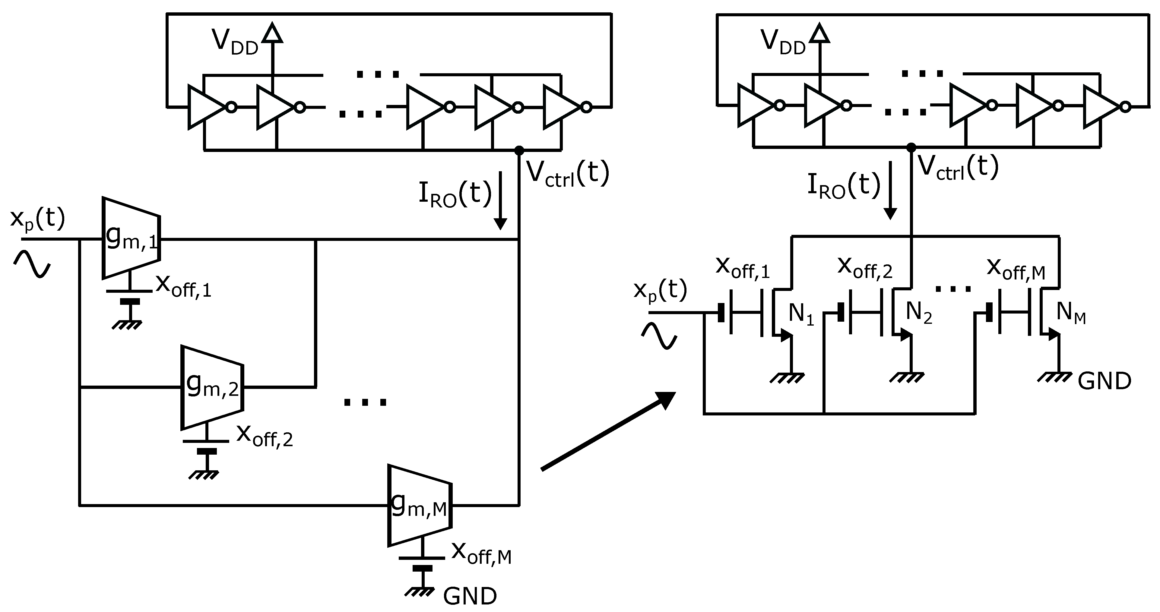
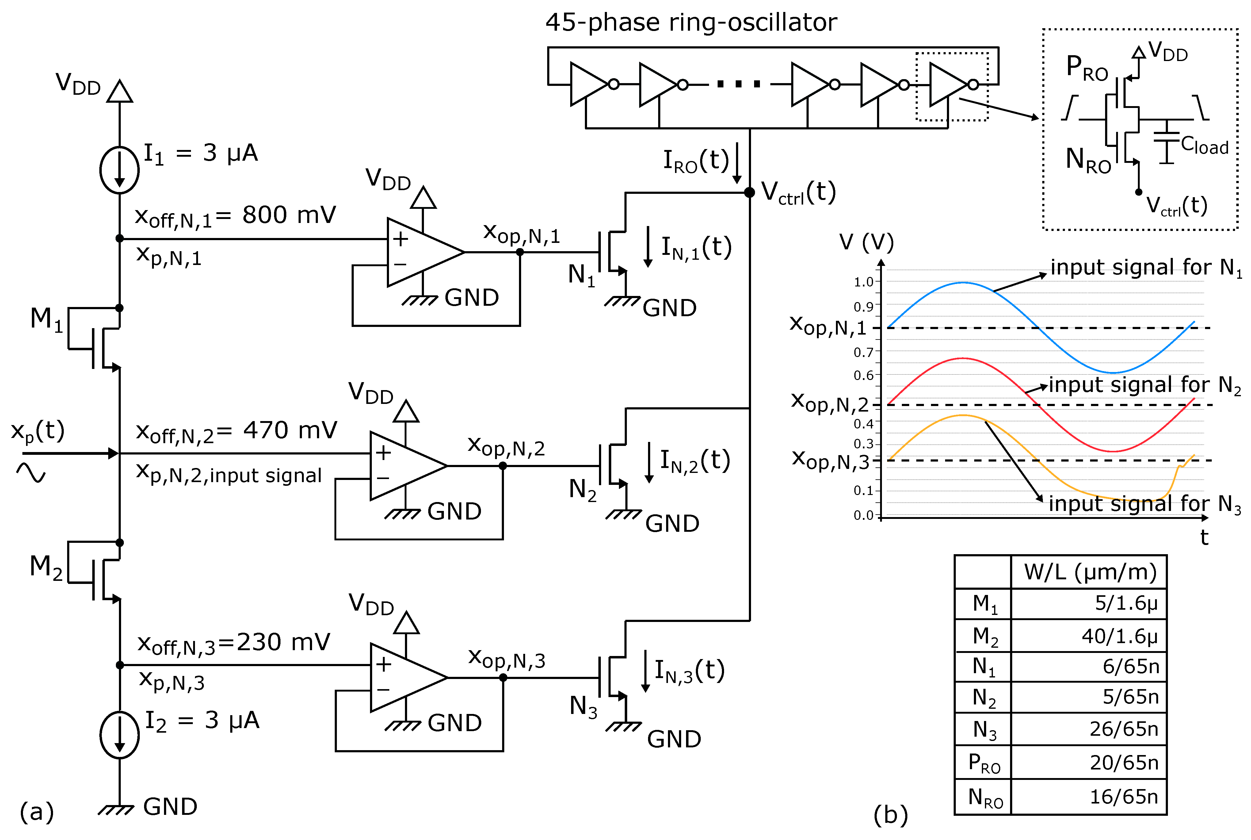
2.2. Proposed Multiple-Transconductor Ring-Oscillator

Figure 4 displays the voltage-to-frequency response of the oscillator simulated above. The ideal linear response has also been plotted. Assuming the ring-oscillator configuration of Figure 2b, we may distinguish between three different regions for the NMOS transistor: the saturated region, where the ring-oscillator shows a behavior approximately linear; and the sub-threshold and ohmic regions, where the nonlinearity is clearly visible. When having the NMOS working at such regions, the harmonic distortion will increase due to the joint action of both the nonlinear voltage-to-current conversion and the nonlinear time delay dependence of the ring-oscillator. This restricts most of the linear operating region to a small input voltage range, which might be suitable for low-swing input voltage applications [37], but not for high-swing ones. To increase the linear voltage range, we can inject more current into the oscillator in the ohmic region to move the curve up (see the arrows in Figure 4), and drain current in the sub-threshold region to move the curve down.
With that purpose in mind, we propose a circuit-level solution to extend the linear response of the ring-oscillator. The solution is based on injecting current into the ring-oscillator with several transconductors, instead of a single one, shifting the saturation regions of them throughout the whole desired input voltage range. On the one hand, we assume that we have at least one device working in saturation at any point of the input voltage range, getting an approximately linear voltage-to-frequency response. On the other hand, we have more flexibility to control the injected current into the ring-oscillator and perform a voltage-to-current conversion that mitigates the distortion due to the nonlinear time dependence of the logic gates. Looking at Figure 4, two current-based operations are needed: injection and draining, requiring respectively both NMOS and PMOS-based devices in the front-end circuit. Thus, the current flowing through the ring-oscillator I RO (t) can be expressed as follows:
I RO ( t ) = i = 1 M I N , i ( t ) j = 1 N I P , j ( t ) ,
where I N , i ( t ) is the current provided by the i-th NMOS device, and I P , j ( t ) is the current drained by the j-th PMOS device.
Using both PMOS and NMOS devices may suppose issues arising from matching and more complexity in making the calibration of the circuit. This is why, for a proof of concept, it was decided to correct and extend only the ohmic region by means of NMOS devices. Several NMOS devices are then connected in parallel. Each of these devices has its own offset component to control the point when they get into the saturation region. Figure 5 depicts a diagram of the proposed solution with a ring-oscillator whose input current is provided by M NMOS devices, where x off , i represents the offset voltage for each of the transconductors. These offset values must be allocated throughout the desired input voltage range to feed the proper current that approximates the inverse current–frequency relation of the ring-oscillator. Linearity is kept mainly because there is always at least one transconductor which is providing sufficient transconductance. Although the rest of transconductors are still providing some current gain, these values are negligible and do not affect the approximation made.
Apart from the mitigation of the nonlinearity, the proposed structure could also be used to enhance the oscillator gain K VCO . Note that, for the conventional approach (Figure 4), the oscillator gain is limited because the transconductor g m drops into the ohmic region and is not able to provide sufficient current to keep increasing the oscillation frequency with the same slope as in the saturation region. With the proposed solution, at any point of the selected input range, there is at least one transconductor providing enough current to keep a linear relation, so that the highest achievable oscillation frequency increases.
Finally, jitter requirements are alleviated due to the open-loop structure, in comparison to closed-loop architectures [21].

3. Results

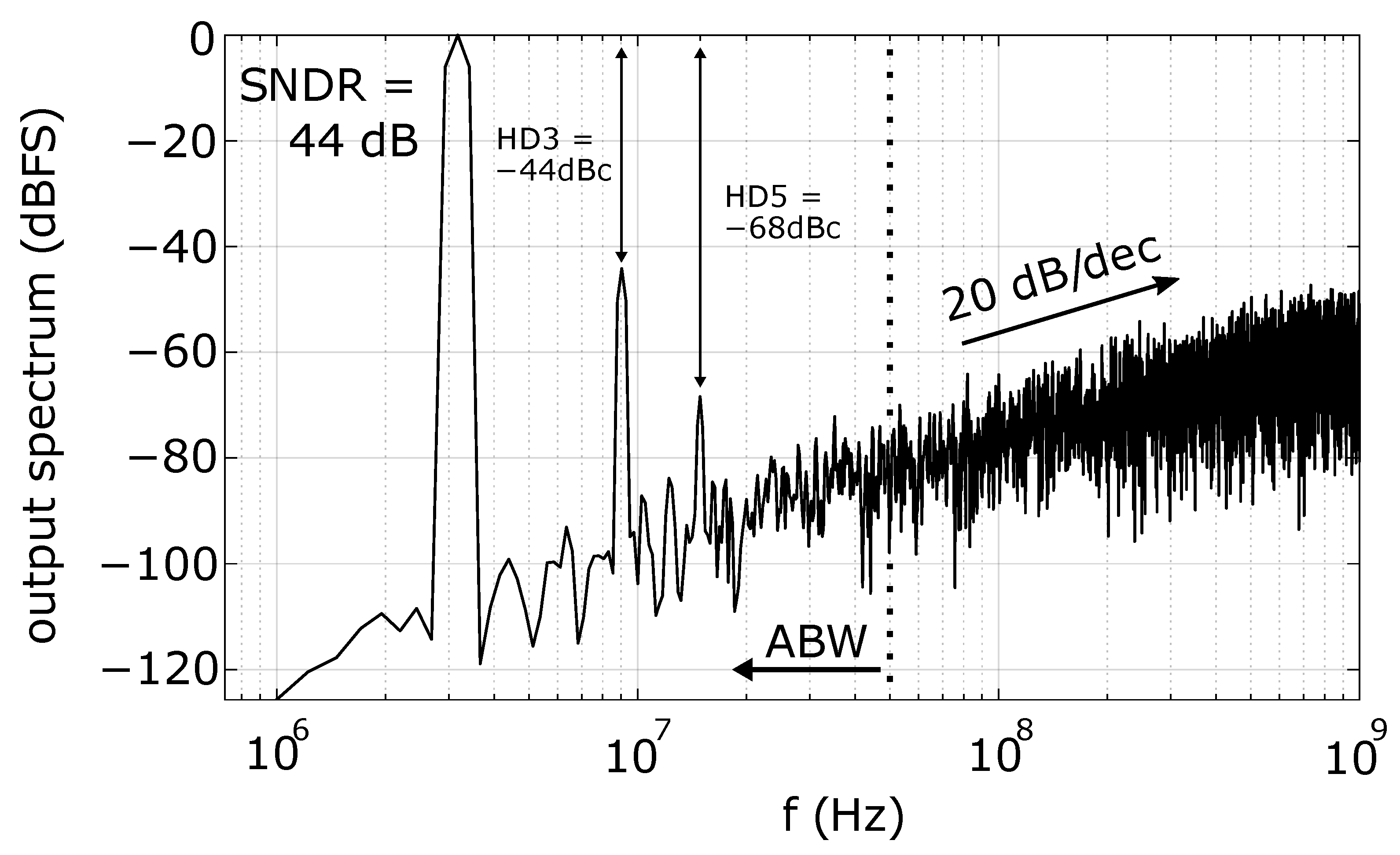
3.1. Circuit Validation

To evaluate the proposed architecture, a version of the circuit of Figure 5 was designed in a 65-nm CMOS process with a pseudo-differential configuration (Figure 2a) and 45 phases in the ring-oscillator. The front-end circuit of the ring-oscillator, together with the circuit used to trim the offset component of each transconductor, is shown in Figure 6. The offset component of the input signal is one of the offset references needed, and the other voltage references are generated by means of fixed bias currents and diode-connected transistors M 1 and M 2 . Due to the limited headroom voltage, M 2 operates in the sub-threshold region. In our case, three offset references were needed, with the values displayed in Figure 6. The size distribution of the transconductors was chosen according to a static behavior, performing a sweep of several transient simulations with different DC input values to get the voltage-to-frequency relation and quantify the nonlinear coefficients.
Low-power opamps connected in a buffer configuration were used to avoid kick-back noise. The opamp does not require high DC gain, hence its design does not lead to a technology scaling issue. The gain-bandwidth product value was 200 MHz and the margin phase was 55 , ensuring the proper operation of the system. Figure 6b illustrates the time response of x op , N , 1 , x op , N , 2 , and x op , N , 3 from a transient simulation where x p ( t ) is a sinusoidal signal. The unitary gain configuration is accomplished totally for x op , N , 1 , x op , N , 2 , and partially for x op , N , 3 , which gets distorted for voltage values lower than the threshold voltage (around 0.25 V). This is not relevant because, for gate voltage values lower than the threshold voltage, N 3 operates in a sub-threshold, and the current provided is negligible and does not significantly modify the approximation to the inverse oscillator’s current-to-frequency function. Opamp’s circuit is depicted in Figure 7, which consists of a two-stage Miller-compensated opamp with low offset (3 mV simulated, which is sufficiently low for proper performance).
Transient simulations were used to check the nonlinearity mitigation. Digital demodulation and sampling logic were modeled in VerilogA language. 10-fF capacitors were placed at the outputs of the ring-oscillator to simulate the input capacitance of the digital logic. Oscillation parameters were kept similar to Figure 3, except K VCO · g m , which was equal to 1.25 GHz/V, slightly higher than before due to linearity compensation. Figure 8 depicts the result of the nominal transient simulation. The HD3 and HD5 were equal to −67 and −75 dBc, respectively, leading to an SNDR of 63 dB (the HD2 value observed in a single-ended configuration was −63 dBc). The distortion is substantially mitigated in comparison to Figure 3. The same simulation was performed with output capacitors of 30 and 50 fF, achieving SNDR values of 62.8 dB and 61.7 dB, respectively, due to the slight decrease in the oscillator gain. The proposed solution achieved a THD value of −66.4 dBc for a differential input of 800 mV pp , Ref. [32] reported a THD chip measurement of −63.6 dBc for a differential input of 566 mV pp , and Ref. [52] reported a THD of −65.3 dBc for a differential input of 400 mV pp in simulation.
Integral nonlinearity (INL) performance, as a static characterization, was also analyzed. The results of a linear ramp test, using the best-fit straight-line approximation, are shown in Figure 9. The single-ended peak-to-peak INL error was [−0.44 0.26], within 1 LSB. In [40], a fully-synthesizable VCO-ADC is presented, where the INL achieved after digital correction was in the range (−1.4 1.49) LSBs and (−1.9 1.6) LSBs for simulation and measurement results, respectively.

3.2. Circuit-Level Impairments

To achieve a correct performance from the proposed solution, proper offset references for each of the transconductors need to be selected. The ring-oscillator might be affected by mismatch effects and PVT variations. This will result in variations in the oscillator current-to-frequency relation and in the required voltage-to-current function. The trimming circuit will be affected by these effects as well, modifying the transconductors’ bias points. To reduce mismatch effects between devices, the diode-connected transistors (M 1 and M 2 ) were designed to be large. To analyze the variation of x off , N , 1 , x off , N , 2 and x off , N , 3 ; and the oscillation frequency due to mismatching a set of 300 runs of Monte Carlo simulations was performed. The SNDR was normally distributed with a mean value of 63 dB and a standard deviation of 1.8 dB, with a worst-case SNDR value, was equal to 59.5 dB.
Apart from the mismatch verification, the impact of PVT variations in the VCO linearity was also checked. We noticed that the function of Figure 4 is mainly shifted throughout the horizontal axis, but its shape did not vary significantly for different PVT conditions. Consequently, centering the input offset in the linear region is the easiest requirement to keep the oscillator working in a linear manner. Figure 10 shows the SNDR values achieved for different PVT cases with the offset of the input signal (x off , N , 2 ) correctly tuned. SNDR degradation can be mainly observed for high temperatures. This degradation occurs when all the transconductors drop into the ohmic region due to the limited V ctrl (Figure 6), which is of special relevance for the FF case where the working linear region is dramatically reduced. To improve the linearity of the proposed solution in these cases, the voltage supply could be increased at the expense of increasing the power consumption or resizing the ring-oscillator at the expense of reducing the gain. All of the simulation results depicted in Figure 10 were obtained with a nominal voltage supply of 1.2 V. The same simulations were repeated including a variation of ±50 mV in the voltage supply. The resulting SNDR values did not differ from the ones shown in Figure 8, which means strong robustness against voltage supply variations.
Additionally, periodic steady-state and phase-noise analyses were performed to evaluate the limitation that the oscillator imposes to the system in terms of phase noise [53]. The estimated value of SNDR regarding the oscillator phase noise was 71 dB, much lower than the quantization noise based SNDR limit observed in Figure 8.

3.3. Calibration Circuit

A calibration circuit is required to correctly select the offset of the input signal x off , N , 2 , approximate the inverse current-to-frequency ring oscillator’s function, and keep proper linearity. With that purpose in mind, we propose to use a digital foreground calibration circuit enabled periodically. Therefore, static power is not increased. The circuit is depicted in Figure 11. The idea is measuring the rest oscillation frequency f o , identifying the PVT operating point of the prototype and correctly selecting the best input signal offset, similar to what was done for Figure 10 elaboration. The rest oscillation frequency is measured by means of a digital delay chain (NAND gates) that measures the semiperiod of the oscillating signal coming from one of the phases of the ring-oscillator. The outputs of the NAND gates are stored with flip-flops, whose outputs are thermometically encoded and represent an estimation of the semiperiod of f o . This digital estimation gets into a Look-Up-Table (LUT) with previously defined values that select the best offset of the input signal. This offset value is finally controlled by means of an opamp whose output offset component can be digitally tuned.

4. Discussion

The proposed architecture does not add extra relevant power consumption. The main contributor to the power breakdown is the oscillator (1.5 mW per oscillator—in line with other previous publications). The power consumption of each opamp is of 115 μ W, and the branch needed to generate the offset references consumes 3.6 μ W. As a consequence, the power consumption associated with the extra circuitry for linearization is less than 19% of the total required power, while, in [32], it is 60%. Although this power estimation will no doubt increase in an experimental prototype, it is expected that the power ratio between these elements remains. In relation to the area, it is not expected that our solution adds extra area growth in comparison to other digital calibration techniques.
The architecture in [32] introduces a VCO-based nonuniform sampling (NUS) ADC, which involves on-chip nonlinearity estimation and off-chip nonlinearity correction embedded within a non-uniform digital signal processing (DSP). The area of the set of structures dedicated to the calibration occupies almost the same of the ADC itself: 0.13 mm 2 and 0.14 mm 2 , respectively. In [36], a reconfigurable CTSDM for analog-to-digital conversion is presented with an on-chip digital background calibration and self-canceling dither techniques. The calibration unit occupies 64% of the area of the whole chip and the voltage-to-current converter and the ring-oscillator consume less than a fifth part of the total power dissipation [54]. Our solution for nonlinearity mitigation does not involve background continuous intensive digital operations and is performed in the analog domain, reducing the required power consumption and also the occupied area.
The VCO-based open-loop configuration ADC in [37] presents a resistive network to tune the ring-oscillator voltage-to-frequency function and reduce harmonic distortion. The principle of the resistive divider scheme was originally introduced in [39], and compromises ring-oscillator’s gain by attenuating the input amplitude. Our solution does not restrict oscillator’s gain.
The structure explored in [19] contains a VCO as a quantizer within a Δ Σ loop. Nonlinearity is mitigated through a high-gain loop filter. The VCO-based quantizer only occupies 3.7% of the active area and consumes 13% of the total power, but it is hardly extended to low voltage supply environments. While enough voltage supply is granted to allow digital switching in the ring-oscillator, our solution can be implemented for lower voltage supply applications.
Table 1 summarizes the performance of the proposed design and provides a comparison to prior works. Different VCO-based ADCs structures (a fully-synthesizable design [40] is also included), hybrid SAR-VCOs, and traditional Flash and SAR architectures are characterized as competitive alternatives. To achieve a fair comparison between the reference solutions and the proposed design, area, power, and Figure-of-Merit (FoM) values only include the ring-oscillator and the associated linearization blocks for the cases where data are available ( ).

5. Conclusions

A circuit-level solution to linearize ring-oscillators-based ADCs is proposed. The solution is based on making use of several transconductors connected in parallel with different bias conditions to implement a voltage-to-current function that approximates the inverse nonlinear current-to-frequency function of the ring-oscillator. To evaluate the approach, a ring-oscillator-based ADC with the proposed circuit was designed and simulated in 65-nm. Nonlinearity was strongly reduced resulting in an ENOB enhancement of more than three bits for high-swing inputs. Additionally, mismatch effects, PVT variations, and noise impact were assessed. The proposal exhibited great robustness without resorting to a complex circuit design and just requiring simple foreground digital calibration. The new VCO-based ADC structure benefits from important power savings in comparison to state-of-the-art digital calibration circuits conventionally used to mitigate distortion. It is also expected to achieve area savings, but this needs to be confirmed through experimental prototypes. The proposal is particularly intended for high-bandwidth and medium-resolution applications, such as 5G or IoT (Internet-of-Things) modules.

Author Contributions

Conceptualization, L.M.A.-G., V.M., V.K., S.P., L.H. and E.G.; methodology, L.M.A.-G., V.M., V.K., S.P., L.H. and E.G.; software, L.M.A.-G. and E.G.; validation, L.M.A.-G. and E.G.; formal analysis, L.M.A.-G. and E.G.; investigation, E.G.; resources, S.P., L.H. and E.G.; data curation, L.M.A.-G. and E.G.; writing—original draft preparation, L.M.A.-G. and E.G.; writing—review and editing, L.M.A.-G., V.M., V.K., S.P., L.H. and E.G.; visualization, L.M.A.-G. and E.G.; supervision, L.H. and E.G.; project administration, L.H. and E.G.; funding acquisition, S.P. All authors have read and agreed to the published version of the manuscript.

Funding

This research was funded by Project TEC2017-82653-R, Spain.

Data Availability Statement

No new data were created or analyzed in this study. Data sharing is not applicable to this article.

Conflicts of Interest

The authors declare no conflict of interest. The funders had no role in the design of the study; in the collection, analyses, or interpretation of data; in the writing of the manuscript, or in the decision to publish the results.

Abbreviations

ADCAnalog-to-digital converter
CCOCurrent-controlled oscillator
ENOBEffective number of bits
IoTInternet-of-things
VCOVoltage-controlled oscillator
SARSuccessive approximation register
OpampOperational amplifier
TITime-Interleaved
NS-SARNoise-shaping SAR
TINS-SARTime interleaving noise-shaping SAR
Δ Σ Delta-Sigma
CTSDMContinuous-time Σ Δ modulator
VCO-based ADCVoltage-controlled oscillator-based analog-to-digital converter
MASHMulti-stage noise shaping
THDTotal harmonic distortion
PVTProcess, voltage and temperature
ABWAnalog bandwidth
HD3Third harmonic distortion term
HD5Fifth harmonic distortion term
HD2Second harmonic distortion term
SNDRSignal-to-noise-distortion ratio
SNRSignal-to-noise ratio
INLIntegral nonlinearity
LSBLeast significant bit
NUSNonuniform sampling
DSPDigital signal processing
CDFCumulative distribution function

References

  1. Lewyn, L.L.; Ytterdal, T.; Wulff, C.; Martin, K. Analog Circuit Design in Nanoscale CMOS Technologies. Proc. IEEE 2009, 97, 1687–1714. [Google Scholar] [CrossRef]
  2. Zahrai, S.A.; Onabajo, M. Review of Analog-To-Digital Conversion Characteristics and Design Considerations for the Creation of Power-Efficient Hybrid Data Converters. J. Low Power Electron. Appl. 2018, 8, 12. [Google Scholar] [CrossRef] [Green Version]
  3. Weaver, S.; Hershberg, B.; Moon, U. Digitally Synthesized Stochastic Flash ADC Using Only Standard Digital Cells. IEEE Trans. Circuits Syst. Regul. Pap. 2014, 61, 84–91. [Google Scholar] [CrossRef]
  4. Fahmy, A.; Liu, J.; Kim, T.; Maghari, N. An All-Digital Scalable and Reconfigurable Wide-Input Range Stochastic ADC Using Only Standard Cells. IEEE Trans. Circuits Syst. II Express Briefs 2015, 62, 731–735. [Google Scholar] [CrossRef]
  5. Jeon, M.; Yoo, W.; Kim, C.; Yoo, C. A Stochastic Flash Analog-to-Digital Converter Linearized by Reference Swapping. IEEE Access 2017, 5, 23046–23051. [Google Scholar] [CrossRef]
  6. Aiello, O.; Crovetti, P.; Alioto, M. Fully Synthesizable Low-Area Analogue-to-Digital Converters With Minimal Design Effort Based on the Dyadic Digital Pulse Modulation. IEEE Access 2020, 8, 70890–70899. [Google Scholar] [CrossRef]
  7. Park, J.; Hwang, Y.; Jeong, D. A 0.5-V Fully Synthesizable SAR ADC for On-Chip Distributed Waveform Monitors. IEEE Access 2019, 7, 63686–63697. [Google Scholar] [CrossRef]
  8. Cao, Z.; Yan, S.; Li, Y. A 32 mW 1.25 GS/s 6b 2b/Step SAR ADC in 0.13 μm CMOS. IEEE J. Solid-State Circuits 2009, 44, 862–873. [Google Scholar] [CrossRef]
  9. Inerfield, M.; Kamath, A.; Su, F.; Hu, J.; Yu, X.; Fong, V.; Alnaggar, O.; Lin, F.; Kwan, T. An 11.5-ENOB 100-MS/s 8mW dual-reference SAR ADC in 28nm CMOS. In Proceedings of the 2014 Symposium on VLSI Circuits Digest of Technical Papers, Honolulu, HI, USA, 10–13 June 2014; pp. 1–2. [Google Scholar]
  10. Kapusta, R.; Shen, J.; Decker, S.; Li, H.; Ibaragi, E.; Zhu, H. A 14b 80 MS/s SAR ADC With 73.6 dB SNDR in 65 nm CMOS. IEEE J. Solid-State Circuits 2013, 48, 3059–3066. [Google Scholar] [CrossRef]
  11. Morie, T.; Miki, T.; Matsukawa, K.; Bando, Y.; Okumoto, T.; Obata, K.; Sakiyama, S.; Dosho, S. A 71dB-SNDR 50 MS/s 4.2 mW CMOS SAR ADC by SNR enhancement techniques utilizing noise. In Proceedings of the 2013 IEEE International Solid-State Circuits Conference Digest of Technical Papers, San Francisco, CA, USA, 17–21 February 2013; pp. 272–273. [Google Scholar]
  12. Chang, D.; Moon, U. A 1.4-V 10-bit 25-MS/s pipelined ADC using opamp-reset switching technique. IEEE J. Solid-State Circuits 2003, 38, 1401–1404. [Google Scholar] [CrossRef]
  13. Shibata, H.; Taylor, G.; Schell, B.; Kozlov, V.; Patil, S.; Paterson, D.; Ganesan, A.; Dong, Y.; Yang, W.; Yin, Y.; et al. 16.6 An 800MHz-BW VCO-Based Continuous-Time Pipelined ADC with Inherent Anti-Aliasing and On-Chip Digital Reconstruction Filter. In Proceedings of the 2020 IEEE International Solid-State Circuits Conference—(ISSCC), San Francisco, CA, USA, 16–20 February 2020; pp. 260–262. [Google Scholar]
  14. Dortz, N.L.; Blanc, J.; Simon, T.; Verhaeren, S.; Rouat, E.; Urard, P.; Tu, S.L.; Goguet, D.; Lelandais-Perrault, C.; Benabes, P. 22.5 A 1.62GS/s time-interleaved SAR ADC with digital background mismatch calibration achieving interleaving spurs below 70dBFS. In Proceedings of the 2014 IEEE International Solid-State Circuits Conference Digest of Technical Papers (ISSCC), San Francisco, CA, USA, 9–13 February 2014; pp. 386–388. [Google Scholar]
  15. Baert, M.; Dehaene, W. A 5-GS/s 7.2-ENOB Time-Interleaved VCO-Based ADC Achieving 30.5 fJ/cs. IEEE J. Solid-State Circuits 2020, 55, 1577–1587. [Google Scholar] [CrossRef]
  16. Paton, S.; Giandomenico, A.D.; Hernandez, L.; Wiesbauer, A.; Potscher, T.; Clara, M. A 70-mW 300-MHz CMOS continuous-time ΣΔ ADC with 15-MHz bandwidth and 11 bits of resolution. IEEE J. Solid-State Circuits 2004, 39, 1056–1063. [Google Scholar] [CrossRef]
  17. Jie, L.; Zheng, B.; Flynn, M.P. 20.3 A 50MHz-Bandwidth 70.4dB-SNDR Calibration-Free Time-Interleaved 4th-Order Noise-Shaping SAR ADC. In Proceedings of the 2014 2019 IEEE International Solid- State Circuits Conference—(ISSCC), San Francisco, CA, USA, 17–21 February 2019; pp. 332–334. [Google Scholar]
  18. Lin, C.-Y.; Lin, Y.-Z.; Tsai, C.-H.; Lu, C.-H. 27.5 An 80MHz-BW 640MS/s Time-Interleaved Passive Noise-Shaping SAR ADC in 22nm FDSOI Process. In Proceedings of the 2021 IEEE International Solid- State Circuits Conference (ISSCC), San Francisco, CA, USA, 13–22 February 2021; pp. 378–380. [Google Scholar]
  19. Straayer, M.Z.; Perrott, M.H. A 12-Bit, 10-MHz Bandwidth, Continuous-Time ΣΔ ADC With a 5-Bit, 950-MS/s VCO-Based Quantizer. IEEE J. Solid-State Circuits 2008, 43, 805–814. [Google Scholar] [CrossRef]
  20. Cardes, F.; Gutierrez, E.; Quintero, A.; Buffa, C.; Wiesbauer, A.; Hernandez, L. 0.04-mm2 103-dB-A Dynamic Range Second-Order VCO-Based Audio ΣΔ ADC in 0.13-μm CMOS. IEEE J. Solid-State Circuits 2018, 53, 1731–1742. [Google Scholar] [CrossRef]
  21. Huang, S.; Egan, N.; Kesharwani, D.; Opteynde, F.; Ashburn, M. 28.3 A 125MHz-BW 71.9dB-SNDR VCO-based CT ΔΣ ADC with segmented phase-domain ELD compensation in 16 nm CMOS. In Proceedings of the 2017 IEEE International Solid-State Circuits Conference (ISSCC), San Francisco, CA, USA, 5–9 February 2017; pp. 470–471. [Google Scholar]
  22. Zhong, Y.; Tang, X.; Liu, J.; Zhao, W.; Li, S.; Sun, N. An 81.5dB-DR 1.25MHz-BW VCO-Based CT ΔΣ ADC with Double-PFD Quantizer. In Proceedings of the 2021 IEEE Custom Integrated Circuits Conference (CICC), Austin, TX, USA, 25–30 April 2021; pp. 1–2. [Google Scholar]
  23. Xing, X.; Gielen, G.G.E. A 42 fJ/Step-FoM Two-Step VCO-Based Delta-Sigma ADC in 40 nm CMOS. IEEE J. Solid-State Circuits 2015, 50, 714–723. [Google Scholar] [CrossRef]
  24. Dey, S.; Mayaram, K.; Fiez, T. A 12 MHz BW, 80 dB SNDR, 83 dB DR, 4th order CT-ΔΣ modulator with 2nd order noise-shaping and pipelined SAR-VCO based quantizer. In Proceedings of the 2019 IEEE Custom Integrated Circuits Conference (CICC), Austin, TX, USA, 14–17 April 2019; pp. 1–4. [Google Scholar]
  25. Hou, Y.; Chen, Z.; Miyahara, M.; Matsuzawa, A. An Op-amp free SAR-VCO hybrid ADC with second-order noise shaping. In Proceedings of the 2016 IEEE International Conference on Electron Devices and Solid-State Circuits (EDSSC), Hong Kong, China, 3–5 August 2016. [Google Scholar]
  26. Sanyal, A.; Ragab, K.; Chen, L.; Viswanathan, T.R.; Yan, S.; Sun, N. A hybrid SAR-VCO ΔΣ ADC with first-order noise shaping. In Proceedings of the IEEE 2014 Custom Integrated Circuits Conference, San Jose, CA, USA, 15–17 September 2014; pp. 1–4. [Google Scholar]
  27. Xie, Y.; Liang, Y.; Liu, M.; Liu, S.; Zhu, Z. A 10-Bit 5 MS/s VCO-SAR ADC in 0.18-μm CMOS. IEEE Trans. Circuits Syst. II Express Briefs 2019, 66, 26–30. [Google Scholar] [CrossRef]
  28. Ragab, K.; Sun, N. A 12-b ENOB 2.5-MHz BW VCO-Based 0-1 MASH ADC With Direct Digital Background Calibration. IEEE J. Solid-State Circuits 2017, 52, 433–447. [Google Scholar] [CrossRef]
  29. Gutierrez, E.; Hernandez, L.; Cardes, F. VCO-based sturdy MASH ADC architecture. Electron. Lett. 2017, 53, 14–16. [Google Scholar] [CrossRef]
  30. Sacco, E.; Vergauwen, J.; Gielen, G. A 16.1-bit Resolution 0.064-mm2 Compact Highly Digital Closed-Loop Single-VCO-Based 1-1 Sturdy-MASH Resistance-to-Digital Converter With High Robustness in 180-nm CMOS. IEEE J. Solid-State Circuits 2020, 55, 2456–2467. [Google Scholar] [CrossRef]
  31. Maghami, H.; Payandehnia, P.; Mirzaie, H.; Zanbaghi, R.; Zareie, H.; Goins, J.; Dey, S.; Mayaram, K.; Fiez, T.S. A Highly Linear OTA-Less 1-1 MASH VCO-Based ΔΣ ADC With an Efficient Phase Quantization Noise Extraction Technique. IEEE J. Solid-State Circuits 2020, 55, 706–718. [Google Scholar] [CrossRef]
  32. Wu, T.; Chen, M.S. A Noise-Shaped VCO-Based Nonuniform Sampling ADC With Phase-Domain Level Crossing. IEEE J. Solid-State Circuits 2019, 54, 623–635. [Google Scholar] [CrossRef]
  33. Gutierrez, E.; Perez, C.; Hernandez, L.; Cardes, F.; Petrescu, V.; Walter, S.; Gaier, U. A Pulse Frequency Modulation VCO-ADC in 40 nm. IEEE Trans. Circuits Syst. II Express Briefs 2019, 66, 51–55. [Google Scholar] [CrossRef]
  34. Perez, C.; Quintero, A.; Amaral, P.; Wiesbauer, A.; Hernandez, L. A 73dB-A Audio VCO-ADC based on a Maximum Length Sequence Generator in 130nm CMOS. IEEE Trans. Circuits Syst. II Express Briefs 2021. [Google Scholar] [CrossRef]
  35. Gutierrez, E.; Hernandez, L.; Cardes, F.; Rombouts, P. A Pulse Frequency Modulation Interpretation of VCOs Enabling VCO-ADC Architectures With Extended Noise Shaping. IEEE Trans. Circuits Syst. I Regul. Pap. 2018, 65, 444–457. [Google Scholar] [CrossRef]
  36. Taylor, G.; Galton, I. A Reconfigurable Mostly-Digital Delta-Sigma ADC With a Worst-Case FOM of 160 dB. IEEE J. Solid-State Circuits 2013, 48, 983–995. [Google Scholar] [CrossRef]
  37. Nguyen, V.; Schembari, F.; Staszewski, R.B. A 0.2-V 30-MS/s 11b-ENOB Open-Loop VCO-Based ADC in 28-nm CMOS. IEEE J. Solid-State Circuits Lett. 2018, 1, 190–193. [Google Scholar] [CrossRef]
  38. Ahmadi-Farsani, J.; Rosa, J.M.d. Bulk-Input VCO-Based Sigma-Delta ADCs with Enhanced Linearity in 28-nm FD-SOI CMOS. In Proceedings of the 2019 IEEE International Symposium on Circuits and Systems (ISCAS), Sapporo, Japan, 26–29 May 2019; pp. 1–5. [Google Scholar]
  39. Fishani, A.B.; Rombouts, P. Highly linear VCO for use in VCO-ADCs. Electron. Lett. 2016, 52, 268–270. [Google Scholar] [CrossRef] [Green Version]
  40. Unnikrishnan, V.; Vesterbacka, M. Time-Mode Analog-to-Digital Conversion Using Standard Cells. IEEE Trans. Circuits Syst. Regul. Pap. 2014, 61, 3348–3357. [Google Scholar] [CrossRef] [Green Version]
  41. Wulff, C.; Ytterdal, T. A Compiled 9-bit 20-MS/s 3.5-fJ/conv.step SAR ADC in 28-nm FDSOI for Bluetooth Low Energy Receivers. IEEE J. Solid-State Circuits 2017, 52, 1915–1926. [Google Scholar] [CrossRef]
  42. Weaver, S.; Hershberg, B.; Maghari, N.; Moon, U. Domino-Logic-Based ADC for Digital Synthesis. IEEE Trans. Circuits Syst. II Express Briefs 2011, 58, 744–747. [Google Scholar] [CrossRef]
  43. Ding, M.; Harpe, P.; Chen, G.; Busze, B.; Liu, Y.; Bachmann, C.; Philips, K.; van Roermund, A. A Hybrid Design Automation Tool for SAR ADCs in IoT. IEEE Trans. Very Large Scale Integr. (VLSI) Syst. 2018, 26, 2853–2862. [Google Scholar] [CrossRef] [Green Version]
  44. Waters, A.; Moon, U.-K. A fully automated verilog-to-layout synthesized ADC demonstrating 56dB-SNDR with 2MHz-BW. In Proceedings of the 2015 IEEE Asian Solid-State Circuits Conference (A-SSCC), Xiamen, China, 9–11 November 2015; pp. 1–4. [Google Scholar]
  45. Aiello, O.; Crovetti, P.; Sharma, A.; Alioto, M. Fully-Synthesizable Current-Input ADCs for Ultra-Low Area and Minimal Design Effort. In Proceedings of the 2019 26th IEEE International Conference on Electronics, Circuits and Systems (ICECS), Genova, Italy, 27–29 November 2019; pp. 715–718. [Google Scholar]
  46. McConaghy, T.; Palmers, P.; Steyaert, M.; Gielen, G.G.E. Trustworthy Genetic Programming-Based Synthesis of Analog Circuit Topologies Using Hierarchical Domain-Specific Building Blocks. IEEE Trans. Evol. Comput. 2011, 15, 557–570. [Google Scholar] [CrossRef]
  47. Gielen, G.; Eeckelaert, T.; Martens, E.; McConaghy, T. Automated synthesis of complex analog circuits. In Proceedings of the 2007 18th European Conference on Circuit Theory and Design, Sevilla, Spain, 26–30 August 2007; pp. 20–23. [Google Scholar]
  48. Rutenbar, R.A.; Gielen, G.G.E.; Roychowdhury, J. Hierarchical Modeling, Optimization, and Synthesis for System-Level Analog and RF Designs. Proc. IEEE 2007, 95, 640–669. [Google Scholar] [CrossRef]
  49. der Plas, G.V.; Vandenbussche, J.; Gielen, G.G.E.; Sansen, W. A layout synthesis methodology for array-type analog blocks. IEEE Trans. Comput. Aided Des. Integr. Circuits Syst. 2002, 21, 645–661. [Google Scholar] [CrossRef]
  50. Rabaey, J.M. Digital Integrated Circuits: A Design Perspective; Prentice-Hall, Inc.: Upper Saddle River, NJ, USA, 1996. [Google Scholar]
  51. Wang, C.; Tsai, J.; Su, S.; Tsai, J.; Chen, J.; Lou, C. 20.6 An 80MHz-BW 31.9fJ/conv-step Filtering ΔΣ ADC with a Built-In DAC-Segmentation/ELD-Compensation 6b 960MS/s SAR-Quantizer in 28nm LP for 802.11ax Applications. In Proceedings of the 2019 IEEE International Solid- State Circuits Conference—(ISSCC), San Francisco, CA, USA, 17–21 February 2019; pp. 338–340. [Google Scholar]
  52. Borgmans, J.; Rombouts, P. Enhanced circuit for linear ring VCO-ADCs. Electron. Lett. 2019, 55, 583–585. [Google Scholar] [CrossRef] [Green Version]
  53. Tu, C.; Wang, Y.; Lin, T. A Low-Noise Area-Efficient Chopped VCO-Based CTDSM for Sensor Applications in 40-nm CMOS. IEEE J. Solid-State Circuits 2017, 52, 2523–2532. [Google Scholar] [CrossRef]
  54. Taylor, G. Mostly Digital ADCs for Highly-Scaled CMOS Processes. Ph.D. Thesis, University of California, Oakland, CA, USA, 2011. [Google Scholar]
Figure 1. (a) General scheme of a VCO; (b) nonlinear VCO operation; and (c) proposed linearization technique.
Electronics 10 01408 g001
Figure 2. (a) Pseudo-differential configuration for an open-loop VCO-based ADC; (b) circuit built with an N-phase ring-oscillator, level shifters, flip-flops, and XOR gates.
Electronics 10 01408 g002
Figure 3. Distortion due to a nonlinear ring-oscillator in analog-to-digital conversion.
Electronics 10 01408 g003
Figure 4. Voltage-to-frequency conversion function of a conventional ring-oscillator (solid line) and an ideal linear curve estimation (dashed line).
Electronics 10 01408 g004
Figure 5. Proposed multiple-transconductor circuit for a linear ring-oscillator-based analog-to-digital conversion.
Electronics 10 01408 g005
Figure 6. Trimming circuit used to generate the offset references of the ring-oscillator, (a) schematic and (b) device sizes and chronograms.
Electronics 10 01408 g006
Figure 7. Two-stage Miller-compensated opamp of Figure 6, (a) schematic and (b) device sizes.
Electronics 10 01408 g007
Figure 8. Output spectrum of transient simulation of the circuit proposed in Figure 6.
Electronics 10 01408 g008
Figure 9. INL performance of the system with the circuit proposed in Figure 6.
Electronics 10 01408 g009
Figure 10. SNDR variation of Figure 8 due to different PVT conditions. Capital letters indicate devices’ process: ‘S’ means “slow”, ‘F’ means “fast”, and ‘T’ means typical. The first letter refers to NMOS devices and the second one refers to PMOS devices. The nominal voltage supply (1.2 V) is the same for all the cases.
Electronics 10 01408 g010
Figure 11. Scheme of the proposed calibration technique.
Electronics 10 01408 g011
Table 1. Comparison to state-of-the-art.
Parameter[3][9][19][23][25][32] *[36][37] *[38][40]This Work
Meas./Sim.MRMRMRMRSRMRMRMRSRMRSR
Results
Supply [V]1.211.20.9111.20.210.61.2
Process [nm]90281304065656528286565
BW [MHz]105502040520037.50.0611025.650
SNDR [dB]35.89676759.575.75770686250.363
THD [dBc]−74.4−67.7−65.7−80.7−63.6−76−72.5−53.9−66.4
INL [LSB] a −2/0.44−1.9/1.6−0.44/0.26
ENOB5.6710.8510.849.5912.39.1811.3411108.0610.17
Diff. Input
Range [mV]
28020001807151800566800355800600 b 800
Power [mW]34.88402.570.5135.4390.00650.233.3 b 3.69
Area [mm 2 ]0.180.10.420.0170.15570.110.070.026 c
FoM [dB] 1 130.7165154160.9173.9154.5159.8167.7166.4149.2164.3
FoM [fJ/c-s] 2 325643.25004214.9153201.2261423532
LinearizationInv.Digital Δ Σ Two-stepDigitalDigitalDigitalResist.Bulk-DigitalMultiple
techniqueGauss.calib.loopVCO-ADCf-calib.f-calib.b-calib.netw.drivenf-calibtransc.
FoM [dB] 1 = SNDR + 10 l o g 10 (BW/Power). FoM [fF/conv-step] 2 = Power/(2·BW·2 ( S N D R 1.76 ) / 6.02 ), a Referred to single-ended mode. b These area and power consumption values are only for the ADC core, the digital correction block is not included. c This input voltage swing is for a single-ended VCO-ADC architecture. Inv. Gaus. CDF = The inverse of Gaussian Cumulative Distribution Function (CDF). Digital f-calib./b-calib. = Digital foreground-calibration/background-calibration.t Resist. netw. = Resistive network. Multiple transc. = Multiple transconductors.
Publisher’s Note: MDPI stays neutral with regard to jurisdictional claims in published maps and institutional affiliations.

