1. Introduction
DDR synchronous dynamic RAM (SDRAM) has evolved over the years in response to ever increasing demand for speed and lower power consumption. DDR4 has data rates from 1600 Mbps to 3200 Mbps and has a rated voltage of 1.2 V [
1]. The increased data rate results in smaller bit interval, which produces stringent timing requirements. The lower operating voltage of DDR4 reduces the margin for voltage noise in the system. The timing and voltage effects due to defects in the system which were not significant before are becoming more important with the increase in data speeds.
DDR4 uses fine pitch ball grid array (FBGA) packages due to their higher input output terminals density, low package dimensions and less parasitic effects [
2,
3,
4]. These packages have solder balls under the package, which are soldered directly to the printed circuit board. The inspection of solder balls becomes difficult once a device is soldered to the printed circuit board. The reliability of the interconnection between the device package and the printed circuit board remains the weakest link in the reliability of the system. The interconnection is susceptible to faults due to mechanical and thermal stresses in the operating environment.
FBGA package solder balls are susceptible to defects, such as void, crack, and fractures. Voids in solder balls occur during the reflow process and they reduce the mechanical reliability of the solder balls [
5]. Cracks in solder balls occur due to thermal coefficient mismatch between the device package and the printed circuit board. The mismatch causes stress on the solder ball and results in cracks in the solder ball [
6,
7,
8,
9]. These cracks are cumulative in nature and may develop into fractures over the period of time.
The crack does not cause an open in the interconnection between the device package and the printed circuit board. However, it changes the electrical characteristics of the interconnection. The crack introduces a parallel capacitance in the electrical model of the interconnection [
10,
11]. The value of the capacitance depends on the dimensions of the crack and the solder ball. The parallel capacitance attenuates higher frequencies and increases the rise time of the signal. The data eye opening becomes smaller due to degradation of the signal. As the data rate increases there is more degradation of the signal. This decrease in the width of the data eye opening degrades the bit error rate of the data channel and, thus, reduces the reliability of the system.
To see the effect of crack in solder ball on the signal integrity of the DDR4 data channel, the data channel is loaded with a capacitive element [
12]. The value of the capacitive element corresponds to the dimensions of the crack. The data eye is measured for the channel with the capacitive loading and is compared with a channel having no defect. The data eye is used to create bathtub plots for the crack defect data channel and the no defect data channel. The comparison of the bathtub plots show the BER degradation due to crack in solder ball [
13,
14].
Section 2 details the crack defect in FBGA solder ball. The electrical model of a non-defective solder ball and a solder ball with crack defect are presented. The crack in solder ball adds parallel capacitance to the electrical model of the solder ball. The capacitance values due to crack are calculated for cracks of various cross sectional areas.
Section 3 details simulation setup and simulation measurements for a DDR4 data channel having cracked solder ball. The data eye width and voltage margin losses are calculated. The simulations show data eye degradation due to crack in solder ball. The simulations are done for data rates of 2.133 Gbps, 2.666 Gbps and 3.2 Gbps. It is shown that as the data rate increases the data eye width and voltage margin losses increase.
Section 4 details the measurement setup and test fixtures for inspecting the crack effect in a running system. DDR4 RDIMM module is loaded with a capacitor to mimic the crack in solder ball. FPGA based memory controller is used for running a pseudo random binary sequence (PRBS) data pattern on the DDR4 data channel. The data channel is probed at the back of the DIMM socket, as it provides an easily accessible probing point.
Section 5 details measurement results. Two DDR4 data channels are measured for comparison. DQ3 data channel has no defect and the data eye is measured for DQ3. The DQ2 data channel has a crack in solder and a capacitor is loaded on the data line to mimic the crack effect in solder ball. DQ3 and DQ2 data eyes are compared. Bathtub plots are created for both DQ3 and DQ2 data channels. Bathtub plots show how the crack increases the bit error rate for the data channel.
Section 6 is the conclusion of the paper.
2. Crack in Solder Ball
Crack in solder ball can form at the solder ball and device interface, in the solder ball or at the solder ball and printed circuit board interface.
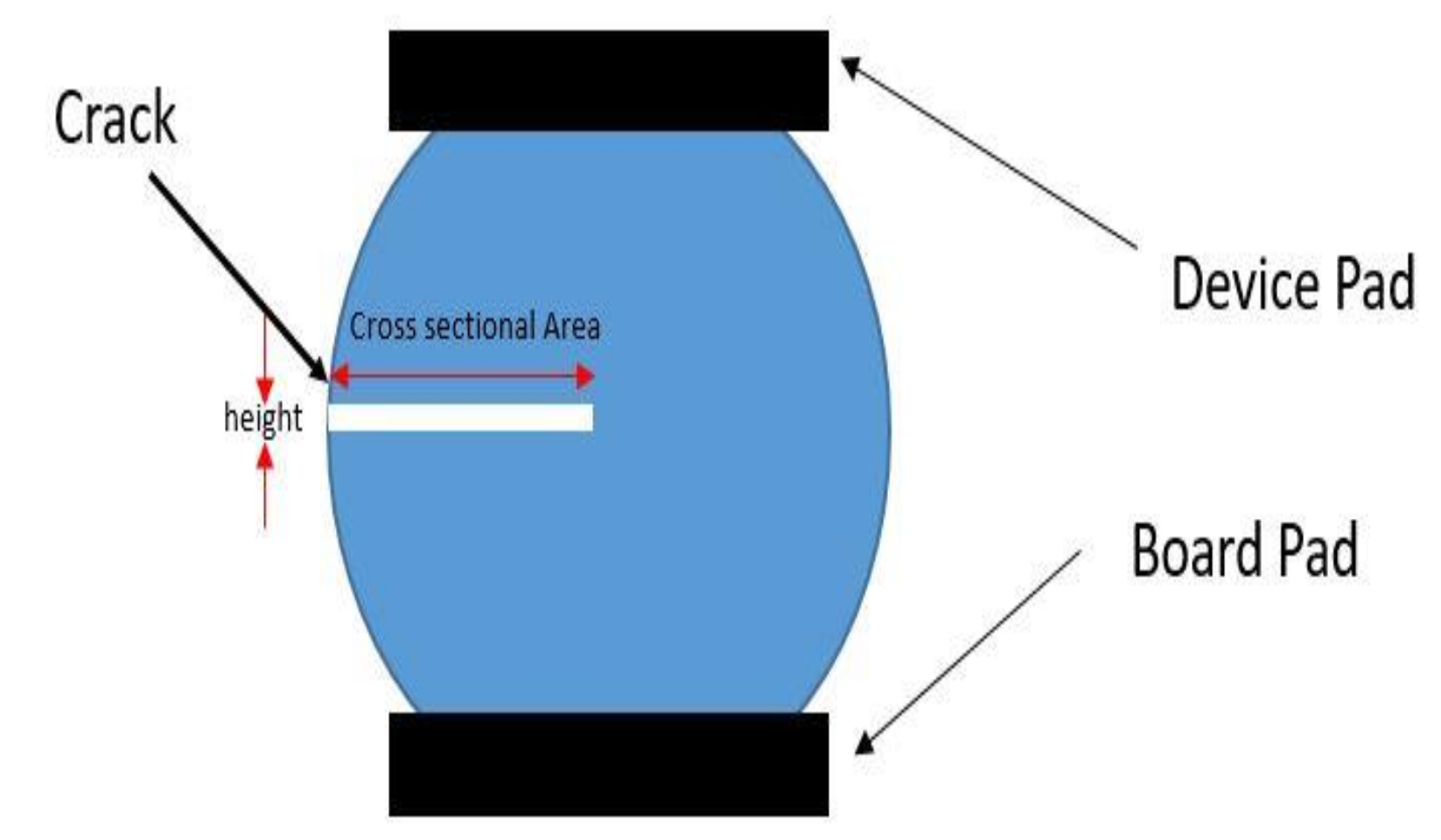
Figure 1 shows crack at the center of the solder ball. The crack divides the solder ball into the connected part and the separated part. The cross section area of the disconnected part can be calculated using the length of the crack.
Figure 1 shows the height of the crack and cross sectional area of the crack.
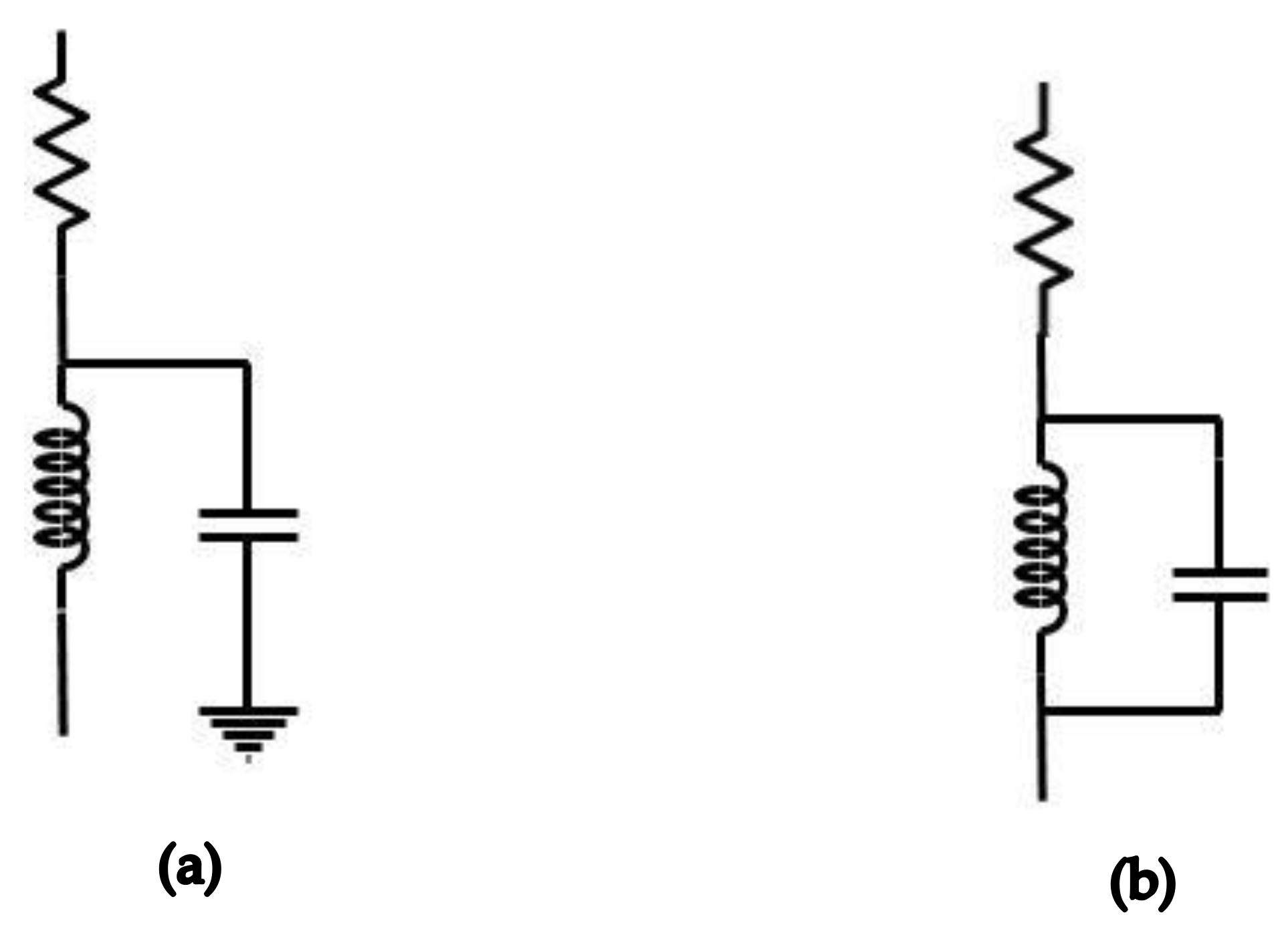
The solder ball electrical model is shown in
Figure 2a [
15]. There is inductance due to the length of the solder ball, parasitic capacitance between the solder ball and the ground. The DC resistance is due to finite conductivity of the solder ball material. At higher frequencies the resistance increases due to the skin effect. The crack in solder ball changes the electrical model of the solder ball as shown in
Figure 2b [
11]. There is parallel capacitance due to the crack, as the crack creates empty space in the solder ball.
The value of the capacitance depends on the cross sectional area of the crack and the height of the crack. The capacitance values for cracks of various lengths and cross sectional areas are shown in
Table 1. The solder ball has diameter of 0.35 mm. The height of the crack is 0.5 nm. The value of the capacitance in
Table 1 is calculated by C = ɛ
r∗ɛ
0∗A
c/d. Where A
c is the area of cross section of the cracked part of the solder ball, d is the height of the crack. ɛ
r is relative permittivity for air and it has a value of 1.0005. ɛ
0 is the permittivity for vacuum and it has a value of 8.854 × 10
−12 F/m [
16].
Table 1 shows that the capacitance due to crack increases as the length of the crack increases.
3. Simulation of Solder Ball Crack in Data Channel
The simulation setup to see the effect of crack in DDR4 data channel and the simulation results are described in this section.
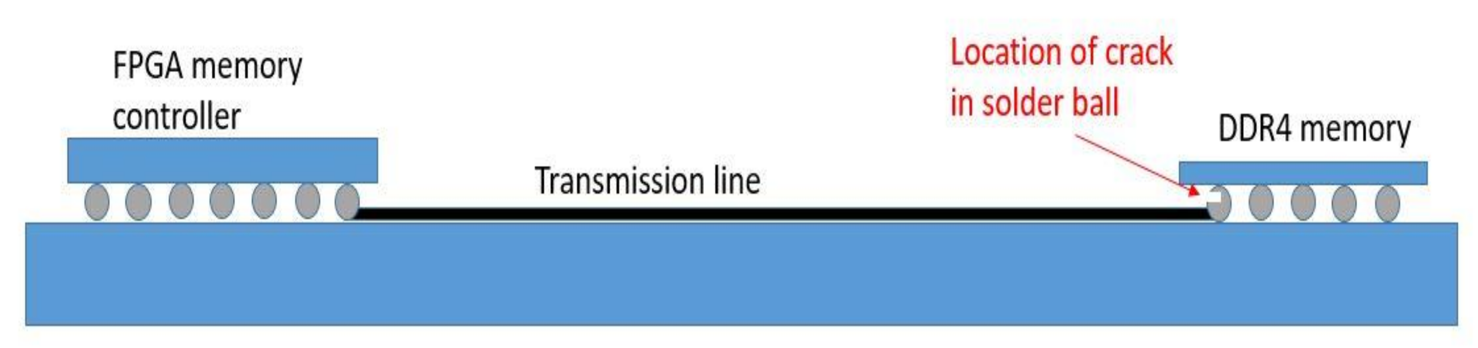
Figure 3 shows location of crack in DDR4 FBGA package solder ball. The crack occurs at the solder ball of the DDR4 data channel. The data eye is measured at the DDR4 receiver. The simulation setup consists of FPGA memory controller connected to DDR4 memory through a transmission line. The vias, DIMM socket, and pcb stack are not included in the simulation. There is no random jitter or noise in the simulation and the simulation qualitatively shows the effect of crack.
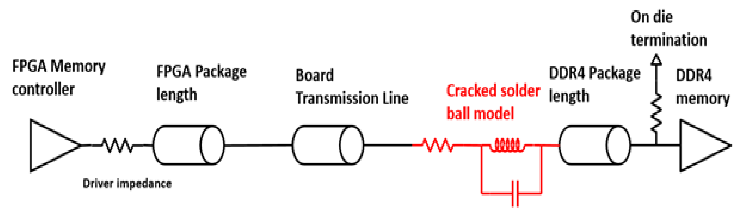
The DDR4 data channel containing the cracked solder ball is shown in
Figure 4. FPGA memory controller IBIS model is used for simulation [
17]. Driver impedance is set to 40 Ohms. The package length describes the pin delay due to trace length in the package. R, L, C pin parameters for FPGA are used. Board transmission line is a microstrip line having 40 Ohms characteristic impedance. The electrical model for cracked solder ball is used in the simulation. The self-resistance of the solder ball is 6.9 milliohm. The self-inductance of the solder ball is 69 picohenry. The capacitance due to crack in the solder ball is 325 picorfarads. DDR4 package length describes the pin delay due to trace length in the package. R, L, and C pin parameters for DDR4 memory are used. The on-die termination for DDR4 is 40 Ohms. Micron DDR4 IBIS model is used [
18].
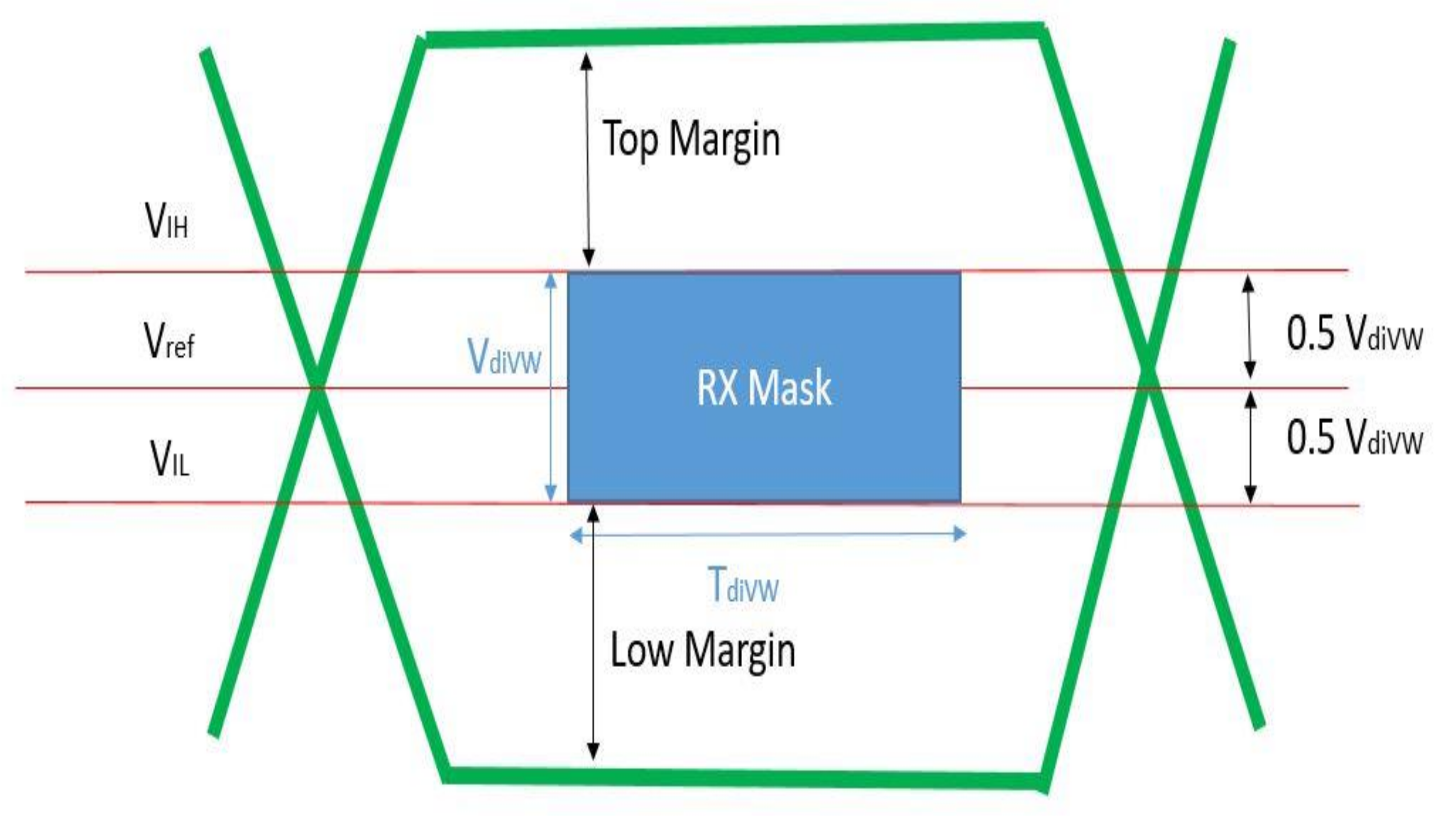
JEDEC standard defines DDR4 receiver mask (RX Mask) as shown in
Figure 5. Time data input valid window (T
divw) defines RX mask along time axis. Voltage data input valid window (V
divw) defines RX mask along voltage axis [
1]. The top margin is defined as the voltage margin between top of the RX mask and top of the data eye. Low margin is defined as the voltage margin between the lower part of the RX mask and low part of the data eye. The width of the data eye is the horizontal opening of the data eye at either V
IH or V
IL, whereas V
IH and V
IL are voltage high and voltage low thresholds, as shown in
Figure 5.
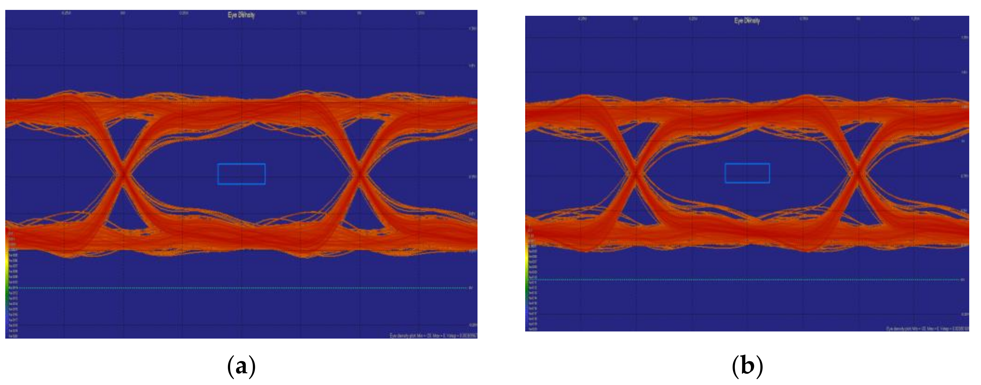
Hyperlynx software was used for simulation. The driver impedance is set to 40 Ohms and the DDR4 termination is set to 40 Ohms. Pseudo random binary sequence (PRBS) signal is applied to the DDR4 data channel and data eye is captured at the DDR4 receiver. The data channel response when there is a cracked solder ball in the data channel is compared with the case when there is no crack in the solder ball. The simulation results show that the cracked solder ball decreases the data eye width, top margin and low margin. This qualitatively shows that there will be increase in bit error rate due to cracks in solder ball.
Figure 6a shows 2.133 Gbps PRBS signal for DDR4 data channel when there is no crack in the DDR4 package solder ball. The rectangle inside the data eye shows the DDR4 receiver RX mask.
Figure 6b shows a data eye when there is a crack in the solder ball. The width of the data eye for
Figure 6a is 0.8598 UI and the width for
Figure 6b is 0.8414 UI, where UI is unit bit interval. The top margin of data eye when there is no crack is 0.1726 V and the top margin is 0.1653 V when there is crack in solder ball. The low margin is 0.1864 when there is no crack and the margin is 0.1726 when there is a crack in solder ball. The crack decreases the data eye width, top margin and low margin. This will result in increased bit error rate.
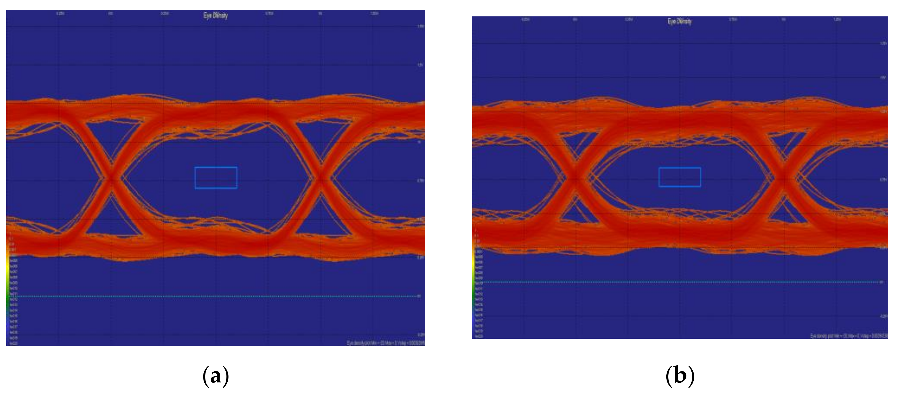
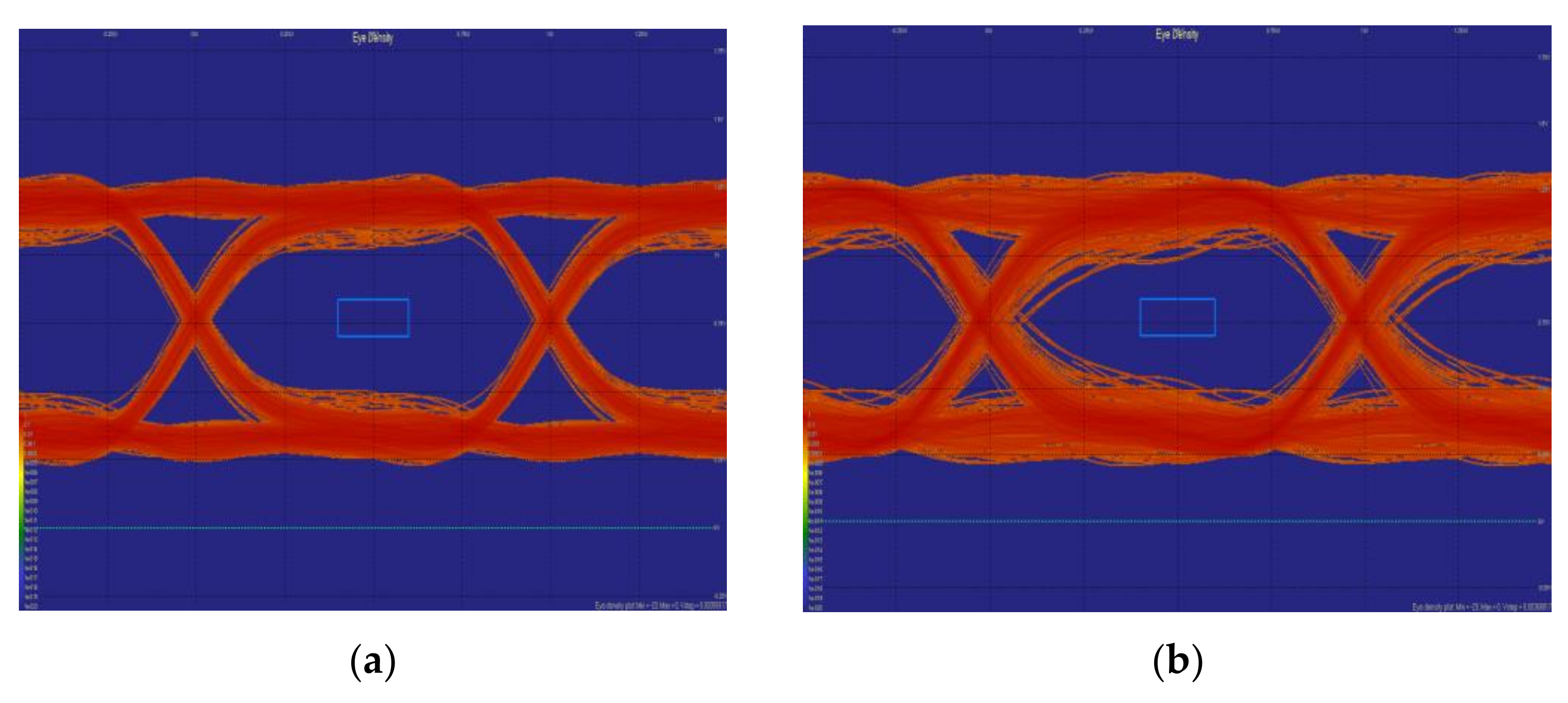
Figure 7 and
Figure 8 show PRBS data eye for data rate of 2.666 Gbps and 3.2 Gbps, respectively. As the data rate increases the data eye becomes more closed due to crack in solder ball. PRBS signal with higher data rate contains higher frequencies and attenuation of these high frequencies due to crack causes more data eye degradation.
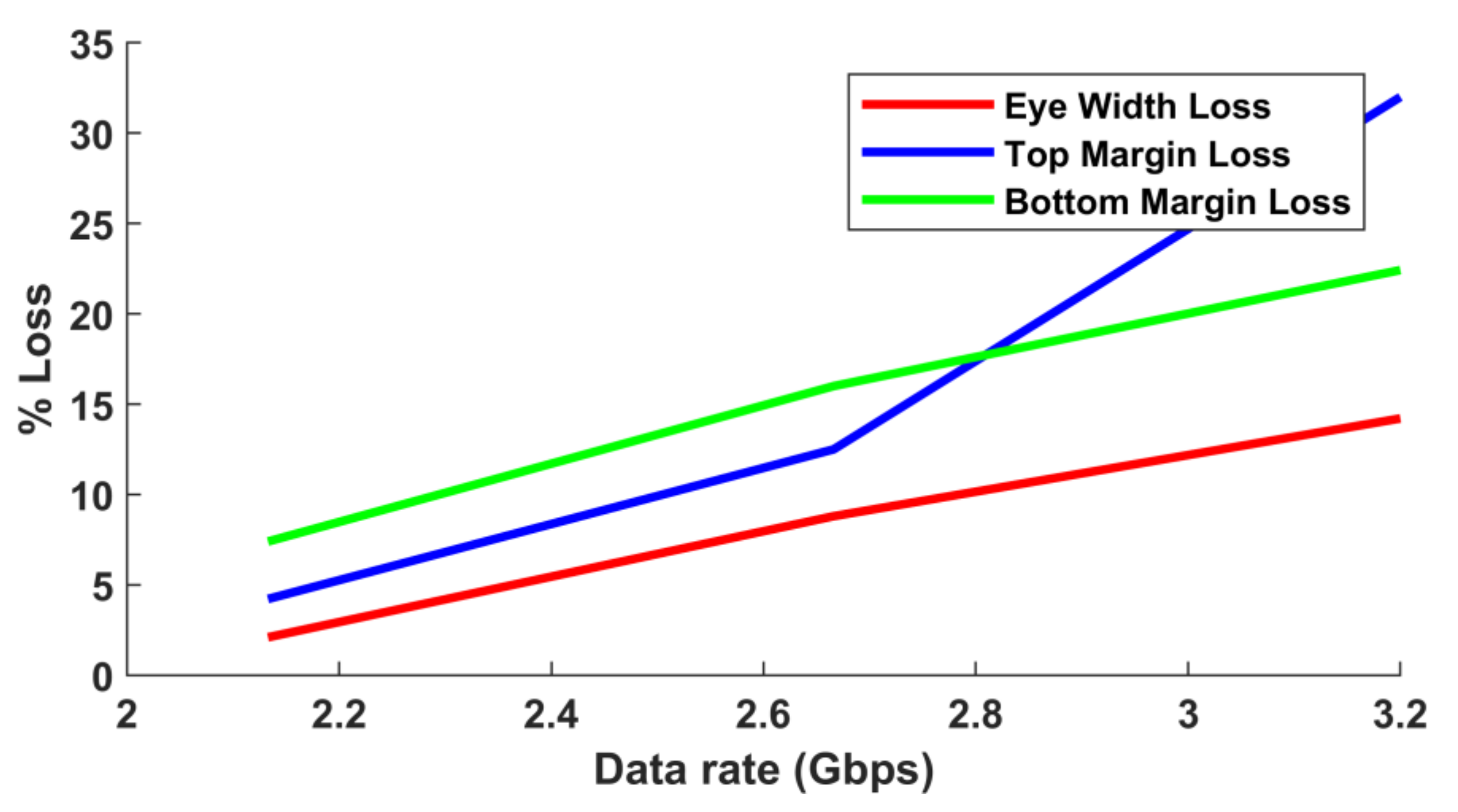
Table 2 shows data eye width, top margin and low margin values calculated for data rates 2.133 Gbps, 2.666 Gbps, and 3.2 Gbps. The percentage loss in data eye width shows the loss due to crack as percentage of the data eye width without crack. Similarly the percentage loss in top margin shows the loss in top margin due to crack as percentage of top margin without crack.
Figure 9 shows effect of crack on data eye for different PRBS signal data rates. Higher data rate means there are higher frequencies in the signal spectrum. There will be more data eye distortion for higher data rates. Eye width loss increases as data rate increases and decreases the available timing margin for the system. Top margin and low margin loss also increases with higher data rate, thus decreasing available voltage margin for the system. This decrease in timing margin and voltage margin will cause bit error rate degradation.
4. Measurement Setup
The defects in FBGA solder ball in running systems are difficult to analyze due to accessibility issues. The solder balls are located under the device package which makes physical inspection difficult except for corner solder balls. The removal of device for inspection may change the condition of solder balls.
The crack in solder ball can be mimicked by loading the data line with a capacitive element [
12]. The value of capacitive element corresponds to the dimensions of the crack.
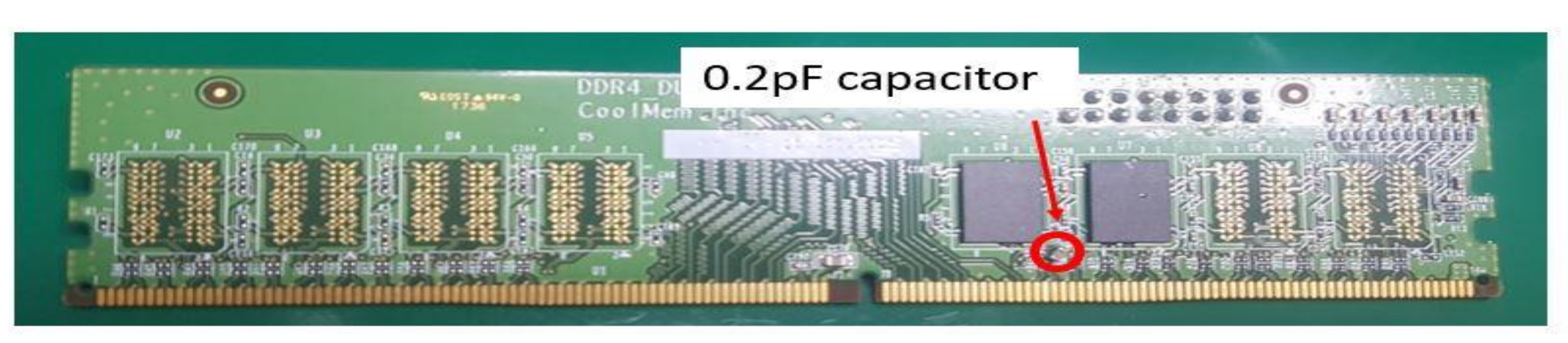
Figure 10 shows a DDR4 RDIMM module with a 0.2 pF capacitor loaded on the data line. The RDIMM module is used for studying the effects of crack in memory systems in running environment. FPGA based memory controller is used for running PRBS pattern on DDR4 memory channel. FPGA board is standard 16 layer board with 50 Ohm transmission line between the FPGA and DDR4 memory.
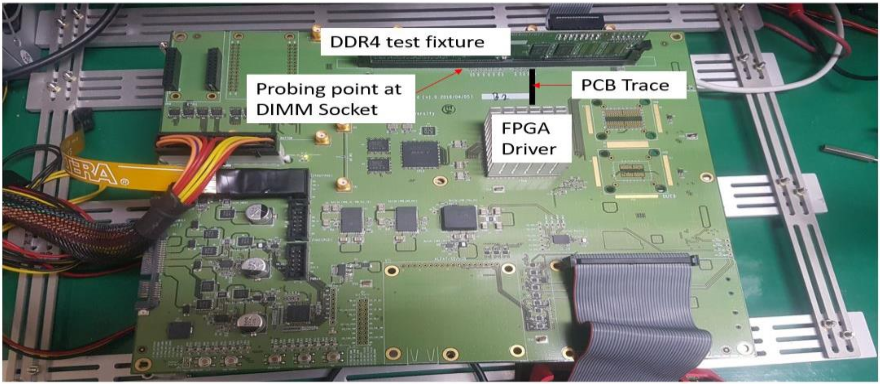
Figure 11 shows the system board with the FPGA and DDR4 RDIMM module. There are discontinuities in the data channel due to FPGA to board interface, vias, routing of transmission line on the layers of board and DIMM socket. These discontinuities also have an effect on the data eye.
The data channel is probed from behind the DIMM socket as shown in
Figure 11. The measurement of the data channel from this point effects the data eye measurement. For analysis two DDR4 data channels are measured. DQ3 channel has no defect in solder ball and DQ2 channel has 0.2 pF capacitor loaded on the data line to mimic the effect of crack in the solder ball. DQ3 channel is compared with DQ2 channel to show the degradation in data eye due to defect. This degradation of data eye results in bit error rate degradation as shown by bathtub plots.
5. Measurement Results
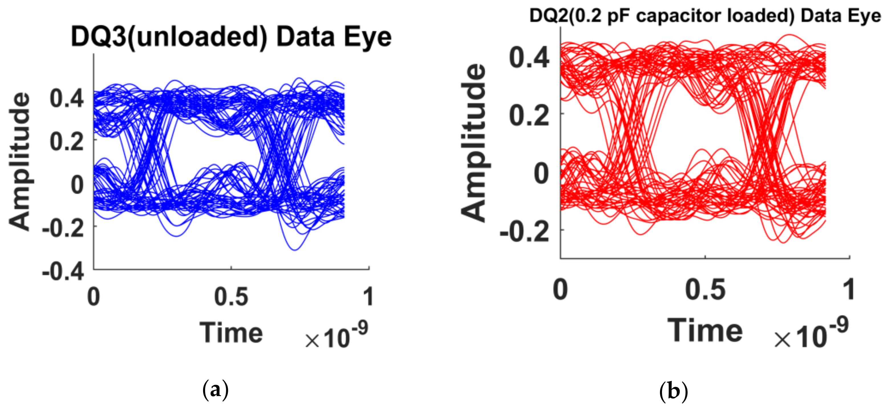
Figure 12a shows DQ3 channel data eye. The width of the data eye is measured at either Vih or Vil. The channel loss gives losses in data channel due to transmission line and discontinuities in the channel. The channel loss is measured by subtracting eye opening from unit bit interval [
19]. For DDR4 operating at 2.133 Gbps the unit interval is 468.8 ps. The data input valid window (V
diVW) for micron DDR4 is 136 mV [
20]. V
diVW is the vertical opening of the DDR4 receiver RX Mask. DQ3 data channel has no defect in solder ball. DQ3 data eye width and channel loss measurements are given as following.
Figure 12b shows DQ2 channel data eye. DQ2 channel has capacitive loading to mimic the crack in solder ball. DQ2 data channel data eye width and data channel loss measurements are given as following.
The comparison of DQ2 and DQ3 shows that DQ2 channel has 36 ps more channel loss due to the eye width decrease introduced by the data eye degradation.
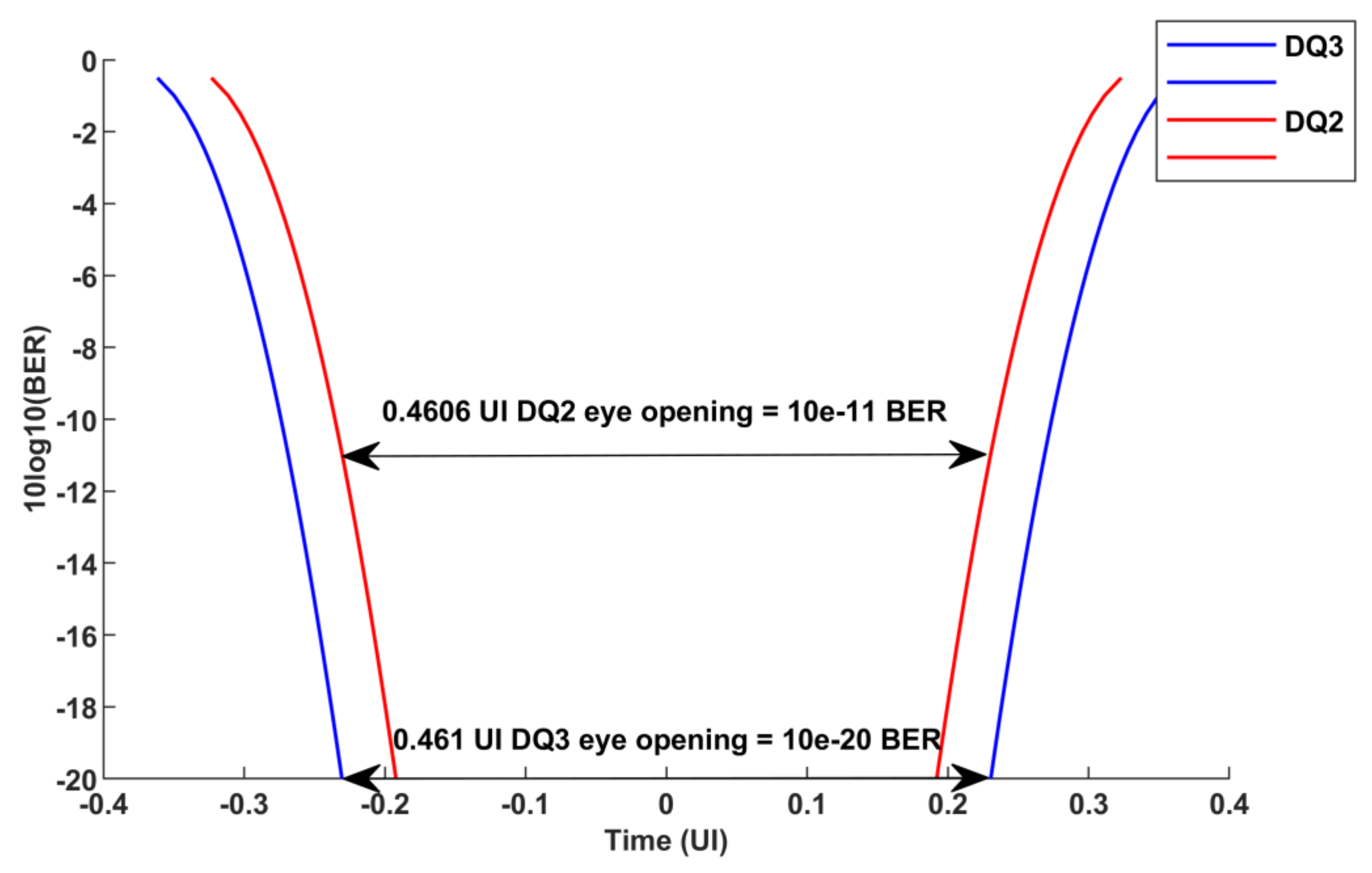
DQ2 and DQ3 data eyes are used to create bathtub plots, as shown in
Figure 13. DQ3 channel bathtub plot shows that it has more eye opening for same bit error rate as DQ2. DQ2 channel with the solder ball defect has smaller eye opening for same bit error rate as DQ3.
Figure 13 also shows that if both DQ2 and DQ3 have eye opening of 0.46 UI, DQ2 has bit error rate of 10e-11 whereas DQ3 has bit error rate of 10e-20. This shows how the crack degrades the bit error rate of DDR4 data channel.


