Article

Pre-Emphasis Pulse Design for Random-Access Memory

Faculty of Engineering, Shizuoka University, Hamamatsu 432-8561, Japan
*
Author to whom correspondence should be addressed.
Electronics 2021, 10(12), 1454; https://doi.org/10.3390/electronics10121454
Submission received: 6 May 2021 / Revised: 9 June 2021 / Accepted: 15 June 2021 / Published: 17 June 2021
(This article belongs to the Special Issue Modeling and Design of Integrated CMOS Circuit)

Abstract

:
This paper describes how one can reduce the memory access time with pre-emphasis (PE) pulses even in non-volatile random-access memory. Optimum PE pulse widths and resultant minimum word-line (WL) delay times are investigated as a function of column address. The impact of the process variation in the time constant of WL, the cell current, and the resistance of deciding path on optimum PE pulses are discussed. Optimum PE pulse widths and resultant minimum WL delay times are modeled with fitting curves as a function of column address of the accessed memory cell, which provides designers with the ability to set the optimum timing for WL and BL (bit-line) operations, reducing average memory access time.

1. Introduction

Nonvolatile random-access memory (NVRAM) or storage class memory are bridging the gap between volatile main memory (DRAM) and nonvolatile NAND flash memory in the memory hierarchy in terms of memory access time to improve memory performance [1,2]. In addition to much faster access time than NAND, NVRAM costs much less than DRAM, helping to keep the computer system cost effective. 3D cross-point memory structure has come to a solution to cost scaling in more advanced nonvolatile memory technology by increasing the number of nonvolatile memory layers [3,4,5,6,7]. A design guideline was proposed for 3D cross-point memory to have a sufficient operation margin to read and write in [8].
Pre-emphasis (PE) pulses are design techniques used to reduce access line delay, especially in large arrays such as 3D NAND [9] and large flat panel display [10]. By driving large RC delay lines with a pulse whose initial period is made with a voltage higher than the target voltage, the entire delay time can be reduced significantly, where the delay time is defined by the farthest point of the line. In [9,10], two calibration methods were proposed, since a precise PE pulse is required even with process variation in the RC time constant. In [11,12], a circuit analysis is discussed to design the PE pulse for minimizing the delay time. Based on the circuit analysis, a PE pulse generator with feedback was proposed in [13].
In this paper, PE pulse design is discussed for NVRAM, where the delay time depends on the column address. Hence, an optimum pulse width of the PE pulse can vary according to the position of the selected memory cell across a selected word-line (WL). In Section 2, the optimum PE pulse width and the minimum delay time are identified as a function of the position on WL in cases of an ideal case with no process variation and an actual case with process variation. Impact of cell current and resistance of decoding transistors is also investigated. In Section 3, the simulated data is compared with measured data for validation. In Section 4, WL behavior with PE pulses is expanded to a three-lines model. Fitting curves with a limited number of parameters are presented for the optimum PE pulse width and the minimum delay time across WL to design the pulses. Colum address dependent PE pulse width is proposed and is applied to a memory system.

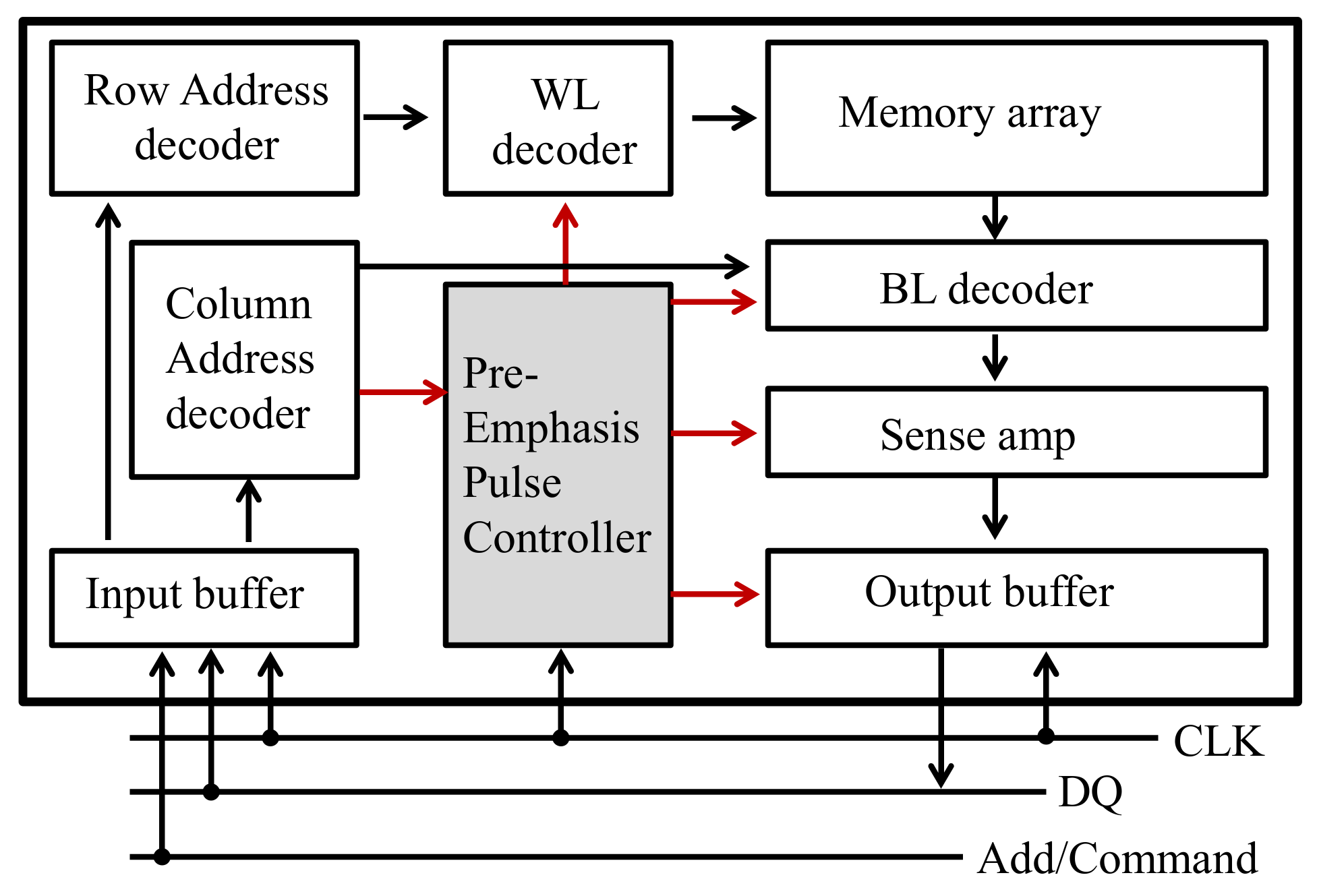
2. Optimum Pre-Emphasis Pulse Design

Figure 1a illustrates a memory array including four different positions N1–N4 across WL, each of which is located at x = 1/4, 1/2, 3/4, and 1. Figure 1b shows simulated waveforms when WL is driven by a PE pulse with an emphasis α of 1.5. As shown in Figure 1c, when the delay time is defined with a voltage window β of 10%, the cell at N2 has the shortest delay time among the four points because the nearest cell at N1 has an overshoot over 10%. Thus, there should be an optimum pulse width per position. An α of 1.5 and a β of 10% are used as the nominal conditions in this paper unless otherwise specified. All the values in this paper that have second as a unit can be scaled by the time constant of WL RC. Thus, arbitrary units are used for time-related parameters.
To see how the PE pulse width TPRE affects the WL delay time TDLY, TPRE is skewed as shown in Figure 2a–d. An α of 1.5 and a β of 10% are demonstrated. When TPRE is shorter than optimum, WL at the target N2 does not reach 90% of the target voltage, resulting in a longer TDLY than the minimum, as shown in Figure 2a. When TPRE is longer than optimum, WL at the target N2 overshoots, resulting in a longer TDLY than the minimum, as shown in Figure 2b. Figure 2c shows the minimum TDLY. As one can imagine, there is a window in TPRE to have the minimum TDLY, as shown in Figure 2d.

2.1. Ideal Case with no Process Variation

When TPRE was varied, there were four patterns in WL waveform at different locations across WL, as summarized in Table 1. In the case of an α of 1.5 and a β of 10%, those patterns are distributed as shown in Figure 3. The vertical axis is TPRE normalized by TOPT, as given by (1), which is the optimum TPRE in case of NAND where the delay time is determined by the farthest location in WL. τ is a time constant given by τ = 4 R C / π 2 .
T O P T = τ ln α α 1
Two boundaries indicate TDLY can be minimized at the location x when TPRE is set between those two boundaries. As expected, the minimum can be realized with pattern 1 or 2. However, below 20% of x, there is no TPRE to realize pattern 1 or 2. This is because an α of 1.5 is too large to realize pattern 1 or 2 with a β of 10%.
Figure 4 shows TDLY as a function of TPRE for x = 1/6, 1/3, 1/2, and 1. A dot indicates the optimum point for the case of NAND. As one can see, All four curves penetrate that point, which means that all points have the same time delay with the same TPRE = TOPT. On the other hand, each point has a different optimum TPRE with its own minimum delay time. For example, the minimum TDLY of x = 1/6 is about 0.5τ, with a TPRE of 0.47τ, whereas the minimum TDLY of x = 1/2 is about 0.8τ, with a TPRE of 0.85τ–1.15τ.
Figure 5a shows which positions can have a shorter delay time when TPRE is set to a specific value. For x < 0.5, the range of optimum TPRE does not include TOPT, resulting in a significant difference in TDLY between the case of TPRE = TOPT and that of an optimum TPRE at each x. Bit-line (BL) delay time starts with WL high. As a result, there is room to start BL access earlier for, e.g., x < 0.8. The memory system taking advantage of that feature will be discussed later. Figure 5b compares TDLY with α = 1.5 and α = 1.2 when TPRE is determined to have the minimum TDLY at each x. A higher pre-emphasis pulse height significantly reduces TDLY at x > 1/3, but increases TDLY a little at x < 1/3 because a larger α does not realize the fastest pattern 1 in Table 1 at the near end of WL.

2.2. Experiment

Figure 6a shows a chip micrograph to validate the SPICE simulation. The test circuits were fabricated in a 0.18 μm 3V CMOS [14]. The RC line is made of multiple units of RC elements, where R and C are given by the poly resistor and MIM capacitor, respectively. Even when a different process technology is used, all the graphs in this paper are still valid because the performance parameters such as TPRE and TDLY are normalized by the RC time constant. Internal nodes can be measured with analog buffers as shown in Figure 6b. Figure 6c is a measured waveform at x = 1/3 and 1.
TDLY is measured with TPRE varied at x = 1/6, 1/3, 1/2, and 1 to determine optimum TPRE for minimizing TDLY at each x. Except for x = 1/6, TPRE has the window whose edge points are plotted in Figure 7a. With such optimum TPRE at each x, TDLY is given as a function of x, as shown in Figure 7b. Table 2 summaries errors of measurement with SPICE.

2.3. Worst Corner under Process Variation

Figure 8 shows TDLY as a function of TPRE under the corner condition of x = 1/2, where RC varies by ±20%. The nominal corner shown by 0% is the same curve as the one in Figure 4. When RC increases, the nominal curve simply shifts in the right top direction of 45°. Therefore, the TDLY − TPRE region can be given as in grey. As a result, the worst corner is determined by the curve in red. Below about 1 for normalized TPRE, the corner of +20% determines TDLY, whereas over about 1 or normalized TPRE, the corner of −20% determines TDLY.
Such a corner is gathered for different locations x, as shown in Figure 9. Every curve has no flat region in terms of TPRE. The vertical line marked as “TOPT” indicates the case when (1) is applied. The graph suggests that TDLY is reduced for x < 1 even with TPRE = TOPT. It also suggests that TDLY can be minimized if one sets TPRE to the lowest point.
Figure 10 shows optimum TPRE vs. x under the nominal and worst corners based on the data of Figure 4 and Figure 8. One can set TPRE with TOPT for x > 1/2. On the other hand, it is good to set TPRE with optimum values for x < 1/2.
Figure 11 shows that x-dependent optimum TOPT can reduce TDLY by 50% at most.

2.4. Impact of Cell Current

3D cross point memory has non-volatile memory cells, each of which flows a cell current. The cell current depends on data 0, 1. When pre-emphasis pulses are used for such memory, an impact of cell current needs to be validated. Figure 12 illustrates WL line model when cells flow at the cell current, which is modeled by Rcel. Let us introduce a parameter γ as Rcel = γ R. When β = 0.1, γ must be greater than 9. Otherwise, the WL voltage at x = 1 cannot reach 0.9E. As γ decreases, TDLY should increase.
As shown in Figure 13, when γ = 10, TDLY increases by 1~7% across WL. However, for γ > 30, TDLY only increases 1% at most. Such an analysis is needed to determine the maximum WL length. Once Rcel is determined, WL length should meet the condition R < Rcel/30.

2.5. Impact of Decoding Transistors

Another concern when designing pre-emphasis pulses for random-access memory is the impact of the driver resistance Rd including decoding transistors and wiring resistance on optimum TPRE and TDLY (see Figure 14). Let us introduce δ to define Rd by Rd = δ R.
Figure 15a–d show optimum TPRE and TDLY at x = 1/6, 1/3, 1/2, and 1 as a function of δ. Optimum TPRE increases in proportion to δ at a rate of about 2.5~3 regardless of x. TDLY has a similar tendency to δ, except when x = 1/6. A finite δ affects TDLY at x = 1/6 most, which decreases TDLY with δ = 0.3~0.5 at most.

3. Discussion

In this section, three-line cases, fitting curves for Optimum TPRE and TDLY, and applications for memory systems are discussed.

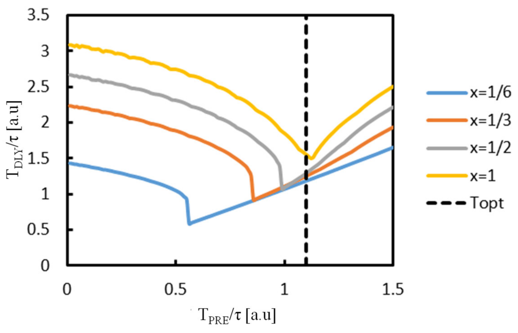
3.1. Three-Line Model

In this section, the general three-line model shown in Figure 16 is studied. The center line is a target delay line, while the next neighbor lines are grounded. The lines have grounded capacitors Cg and coupling capacitors Cc.
The time constant τ of the three-line model is approximated by the sum of RCg and 3RCc;
τ = R Cg + 3 Cc ,
as shown in Figure 17.
SPICE simulations were done for the two cases where Cc:Cg = 1:1 and 100:1 under the condition that τ varies by ±20% and α = 1.2, β = 0.1, resulting in Figure 18. Even though the capacitor ratios are very different, the TDLY vs. TPRE curves normalized by each nominal τ are well matched at four different locations.

3.2. Fitting Curve

To see if one can fit TDLY − x and TPRE − x curves for those two conditions on the cap ratio with single equations with a few fitting parameters, the following equations were investigated.
TPRE = γ1 TOPT_NAND [1 – exp(-x/μ1)],
TDLY = γ2 TDLY_NAND [1 – exp(-x/μ2)],
where TOPT_NAND and TDLY_NAND are given by (5) and (6), respectively, as given for NAND [8,9].
T O P T _ N A N D = τ ln α α 1
T D L Y _ N A N D = τ 9 ln 4 α 3 π β α α 1 8 1 s i n 3 π x 2 ,
When one uses γ1 = 1.2, μ1 = 0.4, γ2 = 0.9, and μ2 = 0.8, the curves are well fit, as shown in Figure 19. “up” and “low” indicate the upper and lower bounds in TPRE to have the minimum delay time. The fitting curve for TPRE vs. x was well done within the upper and lower bounds of both 1:1 and 100:1. Therefore, one needs only two independent fitting parameters per specific α and β. The fitting curve for TDLY vs. x was not as well done as the one for TPRE vs. x, but it did validate that a moderate fitting could be done with only two fitting parameters as well. Thus, such a behavioral model allows designers to set optimum PE pulse widths and resultant delay times.

3.3. Application to Memory System

NVRAM is expected to have much faster access time than NAND or NAND-based solid-state drive, and to have a moderate access time and low bit cos in comparison with DRAM. In such a situation, WL and BL delay times can be as long as multiple clock periods due to large memory arrays. Column-address-dependent memory access can reduce the WL latency when the memory cells located close to the WL decoder are accessed. Figure 20 illustrates a block diagram to realized column-address-dependent memory access. The pre-emphasis pulse controller varies the PE pulse width depending on the column address. The following operations, including BL access and I/O control, can start earlier than the case where the memory cells located at the far side of WL are accessed. The memory controller and CPU can synchronize with it because they know the column address.
When the number of clocks required for WL rise is NWL, which depends on the column address, and that for the other delay times from the address input to the WL decoder and from the memory array to the output buffer is NREST, the total latency of the NVRAM is given by NWL + NREST. Assuming NWL varies from 2 at the nearest cell access to 15 at the farthest cell access based on Figure 19b, one can draw the latency improvement expressed by 1 − (NWL_AVG + NREST)/(NWL_WORST + NREST) as a function of NREST as shown in Figure 21 where NWL_WORST is the worst case NWL when the farthest cell is accessed and NWL_AVG is the average value of NWL between when the farthest and nearest cells are accessed. When NVRAM is designed to have an NREST of 5 to 20, the average latency can be improved by 20–30% with the proposed operation.

4. Conclusions

PE pulsing was studied to assess whether one can reduce the memory access with a PE pulse even when the memory is a random-access type. One can design a PE pulse whose width varies by column address to reduce the WL delay time, even under process variation. The impact of the cell current and the resistance in the decoding path on optimum PE pulse widths and resultant WL delay times are also investigated. Fitting the curves of optimum PE pulse widths and resultant WL delay times of as a function to the column address are demonstrated using only two parameters for each in the case of α = 1.2, β = 0.1, and process variation in τ of ±20%. A block diagram is also proposed to allow column-dependent memory operations to have faster average access.

Author Contributions

Conceptualization, T.T.; methodology, Y.S. and T.T.; software, Y.S.; validation, Y.S. and T.T.; formal analysis, Y.S. and T.T.; investigation, Y.S. and T.T.; writing—original draft preparation, T.T.; writing—review and editing, Y.S. and T.T.; funding acquisition, T.T. Both authors have read and agreed to the published version of the manuscript.

Funding

This research was partially funded by Kioxia Corp.

Acknowledgments

This work is supported by Kioxia Corp., VDEC, Synopsys, Inc., Cadence Design Systems, Inc., Rohm Corp., and the Micron Foundation.

Conflicts of Interest

The authors declare no conflict of interest.

References

  1. Hoya, K.; Hatsuda, K.; Tsuchida, K.; Watanabe, Y.; Shirota, Y.; Kanai, T. A perspective on NVRAM technology for future computing system. In Proceedings of the 2019 International Symposium on VLSI Technology, Systems and Application (VLSI-TSA), Hsinchu, Taiwan, 22 April 2019; pp. 1–2. [Google Scholar]
  2. Strenz, R. Review and Outlook on Embedded NVM Technologies— From Evolution to Revolution. In Proceedings of the 2020 IEEE International Memory Workshop (IMW), Dresden, Germany, 17 May 2020; pp. 1–4. [Google Scholar]
  3. Chien, W.; Ho, H.; Yeh, C.; Yang, C.; Cheng, H.; Kim, W.; Kuo, I.; Gignac, L.; Lai, E.; Gong, N.; et al. Comprehensive Scaling Study on 3D Cross-Point PCM toward 1Znm Node for SCM Applications. In Proceedings of the 2019 Symposium on VLSI Technology, Kyoto, Japan, 9–14 June 2019; IEEE: Piscataway, NJ, USA, 2019; pp. 60–61. [Google Scholar] [CrossRef]
  4. Zhou, J.; Kim, K.-H.; Lu, W. Crossbar RRAM Arrays: Selector Device Requirements During Read Operation. IEEE Trans. Electron Devices 2014, 61, 1369–1376. [Google Scholar] [CrossRef]
  5. Chevallier, C.J.; Siau, C.H.; Lim, S.F.; Namala, S.R.; Matsuoka, M.; Bateman, B.L.; Rinerson, D. A 0. 13 µm 64 Mb multi-layered conductive metal-oxide memory. In Proceedings of the 2010 IEEE International Solid-State Circuits Conference (ISSCC), San Francisco, CA, USA, 7 February 2010; pp. 260–261. [Google Scholar]
  6. Kau, D.; Tang, S.; Karpov, I.V.; Dodge, R.; Klehn, B.; Kalb, J.A.; Strand, J.; Diaz, A.; Leung, N.; Wu, J.; et al. A stackable cross point Phase Change Memory. In Proceedings of the 2009 IEEE International Electron Devices Meeting (IEDM), Baltimore, MD, USA, 7 December 2009; pp. 1–4. [Google Scholar]
  7. Kawahara, A.; Azuma, R.; Ikeda, Y.; Kawai, K.; Katoh, Y.; Hayakawa, Y.; Tsuji, K.; Yoneda, S.; Himeno, A.; Shimakawa, K.; et al. An 8 Mb Multi-Layered Cross-Point ReRAM Macro With 443 MB/s Write Throughput. IEEE J. Solid-State Circuits 2013, 48, 178–185. [Google Scholar] [CrossRef]
  8. Yu, S.; Deng, Y.; Gao, B.; Huang, P.; Chen, B.; Liu, X.; Kang, J.; Chen, H.-Y.; Jiang, Z.; Wong, H.-S.P. Design guidelines for 3D RRAM cross-point architecture. In Proceedings of the 2014 IEEE International Symposium on Circuits and Systems (ISCAS), Melbourne, Australia, 1 June 2014; pp. 421–424. [Google Scholar] [CrossRef]
  9. Jeong, W.; Im, J.-W.; Kim, D.-H.; Nam, S.-W.; Shim, D.-K.; Choi, M.-H.; Yoon, H.-J.; Kim, D.-H.; Kim, Y.-S.; Park, H.-W.; et al. A 128 Gb 3b/cell V-NAND Flash Memory With 1 Gb/s I/O Rate. IEEE J. Solid-state Circuits 2016, 51, 204–212. [Google Scholar] [CrossRef]
  10. Bang, J.-S.; Kim, H.-S.; Yoon, K.-S.; Lee, S.-H.; Park, S.-H.; Kwon, O.; Shin, C.; Kim, S.; Cho, G.-H. 11.7 A load-aware pre-emphasis column driver with 27% settling-time reduction in ±18% panel-load RC delay variation for 240 Hz UHD flat-panel displays. In Proceedings of the 2016 IEEE International Solid-State Circuits Conference (ISSCC), San Francisco, CA, USA, 31 January 2016; pp. 212–213. [Google Scholar] [CrossRef]
  11. Matsuyama, K.; Tanzawa, T. Design of Pre-Emphasis Pulses for Large Memory Arrays with Minimal Word-Line Delay Time. In Proceedings of the 2019 IEEE International Symposium on Circuits and Systems (ISCAS), Sapporo, Hokkaido, Japan, 26 May 2019; pp. 1–5. [Google Scholar] [CrossRef]
  12. Matsuyama, K.; Tanzawa, T. A Circuit Analysis of Pre-Emphasis Pulses for RC Delay Lines. IEICE Trans. Fundam. Electron. Commun. Comput. Sci. 2021, E104.A, 912–926. [Google Scholar] [CrossRef]
  13. Matsuyama, K.; Tanzawa, T. A Pre-Emphasis Pulse Generator Insensitive to Process Variation for Driving Large Memory and Panel Display Arrays with Minimal Delay Time. In Proceedings of the 2019 IEEE Asia Pacific Conference on Circuits and Systems (APCCAS), Bangkok, Thailand, 11 November 2019; pp. 45–48. [Google Scholar]
  14. VLSI Design and Education Center (VDEC). Available online: http://www.vdec.u-tokyo.ac.jp/English/index.html (accessed on 1 May 2021).
Figure 1. (a) Memory array, (b,c) WL behavior at x = 1/4, 1/2, 3/4, and 1 with PE pulse where α and β are 1.5 and 0.1, respectively.
Electronics 10 01454 g001
Figure 2. WL behavior at N2 with TPRE of 0.6τ (a), 1.25τ (b), and 0.9τ (c), and TDLY vs. TPRE (d).
Electronics 10 01454 g002
Figure 3. WL waveform pattern across x and TPRE. 1–4 areas in the figure indicate pattern 1–4 in Table 1, respectively.
Electronics 10 01454 g003
Figure 4. TDLY as a function of TPRE for x = 1/6, 1/3, 1/2, and 1.
Electronics 10 01454 g004
Figure 5. TDLY as a function of x. TDLY is compared (a) between the case where TPRE is set at TOPT at all x and the case where TPRE is determined to have the minimum TDLY at each x and (b) between α = 1.5 and α = 1.2 when TPRE is determined to have the minimum TDLY at each x.
Electronics 10 01454 g005
Figure 6. (a) die photo, (b) block diagram of the test circuit, and (c) voltage waveform at x = 1 and 1/3 (α = 1.5).
Electronics 10 01454 g006
Figure 7. Optimum TPRE vs. x (a) and TDLY vs. x (b).
Electronics 10 01454 g007
Figure 8. TDLY as a function of TPRE under the worst corner.
Electronics 10 01454 g008
Figure 9. TDLY vs. TPRE at x = 1/6, 1/3, ½, and 1 under the worst corner.
Electronics 10 01454 g009
Figure 10. Optimum TPRE vs. x under the nominal and worst corners.
Electronics 10 01454 g010
Figure 11. TDLY vs. x under the worst corner.
Electronics 10 01454 g011
Figure 12. WL line model when cells flow at cell current.
Electronics 10 01454 g012
Figure 13. TDLY vs. γ with x-dependent optimum TPRE.
Electronics 10 01454 g013
Figure 14. WL line model when the driver resistance is considered.
Electronics 10 01454 g014
Figure 15. Optimum TPRE and TDLY vs. δ for x = 1/6 (a), 1/3 (b), 1/2 (c), and 1 (d).
Electronics 10 01454 g015
Figure 16. General three-line model with grounded cap Cg and coupling cap Cc.
Electronics 10 01454 g016
Figure 17. Effective time constant model.
Electronics 10 01454 g017
Figure 18. TDLY vs. TPRE for the models with different cap ratios under the worst case where τ varies by ±20% (α = 1.2, β = 0.1).
Electronics 10 01454 g018
Figure 19. Fitting and simulated curves for TPRE vs. x (a) and TDLY vs. x (b), whose data is taken from Figure 18.
Electronics 10 01454 g019
Figure 20. Block diagram of a proposed NVRAM.
Electronics 10 01454 g020
Figure 21. Latency improvement with the proposed NVRAM operation.
Electronics 10 01454 g021
Table 1. WL waveform pattern.
PatternWhat Point Determines TDLYWaveform
1First rising point in higher order behavior Electronics 10 01454 i001
2First rising point in single order behavior Electronics 10 01454 i002
3First falling point in higher order behavior Electronics 10 01454 i003
4Second rising point in higher order behavior Electronics 10 01454 i004
Table 2. Error between measured TDLY and simulated TDLY at each x.
xError [%]
1/612.2
1/36.0
1/22.0
11.5
Publisher’s Note: MDPI stays neutral with regard to jurisdictional claims in published maps and institutional affiliations.

