Abstract
This paper proposes a three-port Zeta-KY dc-dc converter which is fed with hybrid sources like photovoltaic (PV) cells and batteries. The converter proposed here is a multi-input single-output (MISO) structure which harnesses the benefits of Zeta and KY converters. The combination of these converters is highly advantageous since the Zeta converter provides lesser output voltage ripples with high gain and the KY converter topology suits well for withstanding load transients. The KY converter used in this research work is subjected to a topological change to facilitate bidirectional power flow. The bidirectional flow is essential to save the excess power in PV source in batteries during low load conditions. This novel multiport topology with bidirectional facility is first of its kind and has not been discussed earlier in the research arena. In the proposed work, two control algorithms are developed and deployed: the first one ensures the maximum power extraction from the PV and the second one maintains constant dc bus voltage and manages bidirectional power flow. MATLAB Simulink and hardware prototype of the proposed system has been realized for a 72 V dc bus and a 500 W electric vehicular drive. The simulation and experimental results reveal that the proposed system is viable for medium power electric shuttle applications. The proposed system is subjected to various test cases and it is observed that the source and load intermittencies are catered very well by the proposed three port Zeta-KY converter. The developed multiport converter is feasible for renewable energy applications.
1. Introduction
Power generation through distributed sources like photovoltaic, wind energy conversion systems, fuel cells are fast emerging. These alternative energy sources can be part of a distributed power generation (DPG) system. The major challenge that DPG faces is the non-continuous power output due to the intermittent behavior of the renewable sources. For example, the PV system power output changes with respect to solar irradiation level and temperature profile throughout the day. Likewise, the wind energy conversion system (WECS) output changes with respect to the wind velocity. To maximize the available power at output, the power converter control unit embodies a specialized algorithm called maximum power point tracker (MPPT). Its use in a micro grid or nano grid adds complexity to the energy conversion process by requiring dedicated individual control circuit in each renewable energy source. Moreover, the MPPTs are only mandated for operating the PV system to its peak power and as such voltage regulation at the output is not possible. Therefore, the research on proposing multiport converters with optimal switching topology and control algorithm has attracted significant attention in the research forum.
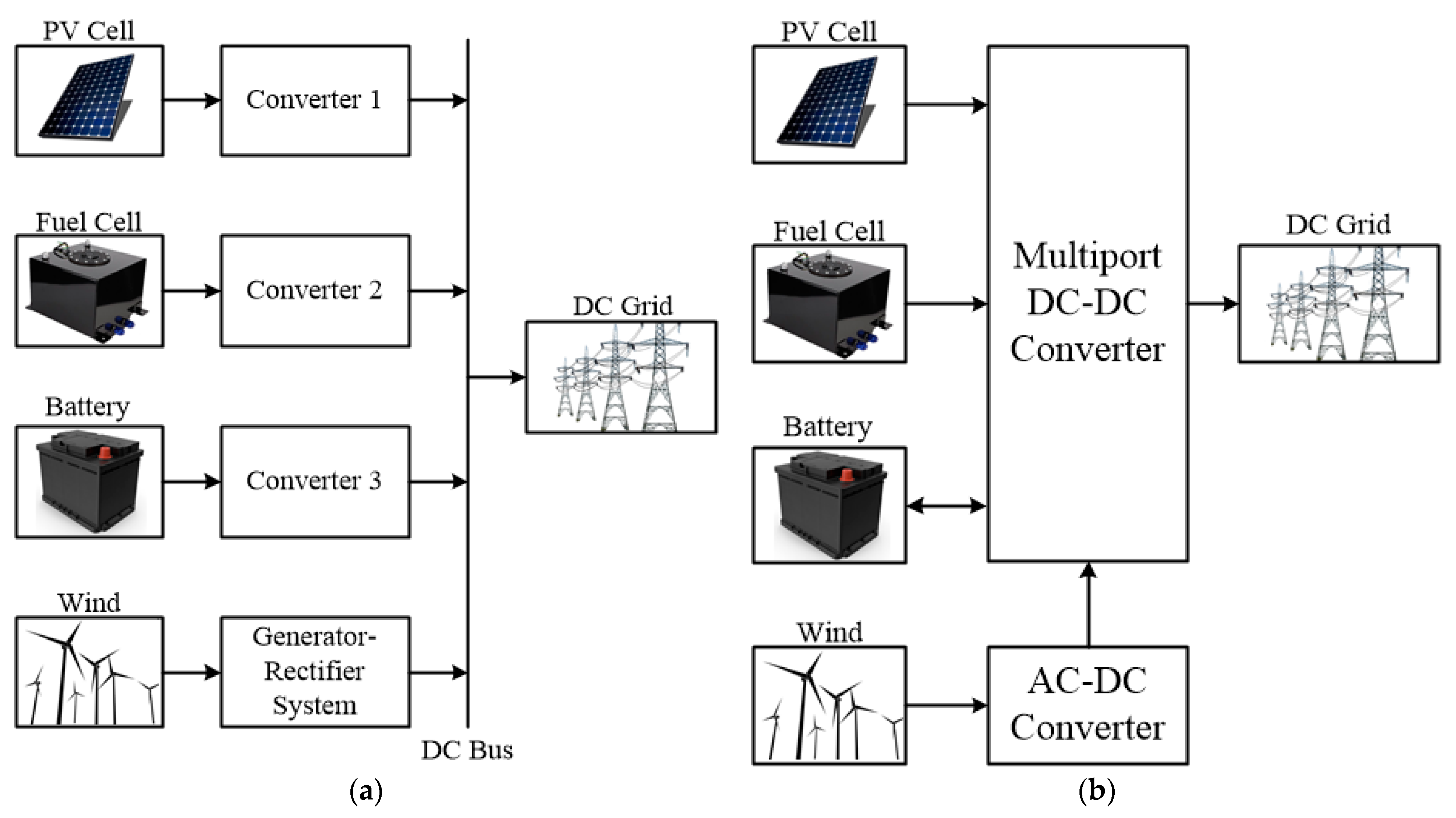
Voltage multiplier cells and coupled inductors were employed in renewable energy systems with isolated structure [1]. Again, an isolated structure with impedance source dc-dc converter was proposed with a greater number of passive components [2]. However, the converter was bulky with isolation transformer and had a higher number of capacitors in the input side. A converter was designed in [3] by Onar et al. for power management of battery and ultra-capacitor energy storage system was integrated although this could not be used for longer period. The discharge rate was larger than the usual batteries. With these drawbacks of the ultra-capacitors they are not mostly preferable. A high frequency dual bridge series resonant dc-dc converter was designed by Xiaodong Li et al. [4] in which an isolated section was provided for conversion process. These converters stated in [1,2,3,4] had drawbacks such as possession of dc link ultra-capacitors and integrated magnetic structures which adds up to the complexity in control schemes. Later on, the dc converters were designed to be sourced from multiple renewable energy sources called as multi input multiple converters. These drawbacks of isolation transformers were eliminated in other studies [5,6] and efficient power conversion is obtained but with a greater number of conversion topologies. An isolated three level dc power conversion was proposed by Dusmez et al. [7] that was cost effective, but the number of components used was more and had different levels of power conversion. In addition, in [8,9], the cascaded H bridge structures were proposed for multiple energy sources, but the power conversion process involved multiple dc links in their converters and increased the overall volume of the dc converter. In other proposed research works [1,2,3,4,5,6,7,8,9], multiple energy sources were fed to dc-dc converters either to feed dc or ac loads as shown in Figure 1a.
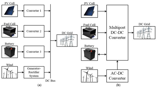
Figure 1.
Block diagram of (a) conventional multi input multiple converter system and (b) multiport converter.
The dc-dc converters were developed from the basic buck, boost or buck boost converters that employed dc link voltages and isolation transformers. The converters employed multiple converters for multiple energy sources. Few converters from the above cited research works also employed a greater number of components and complex control topologies for the power conversion. For eliminating these drawbacks that incurred in multi input multiple converters, the dc-dc converters named multiport converters (MPC) emerged into the scenario of dc power conversion. These multiport converters employed a single converter with multiple inputs and multiple outputs depending on the sources and load. These types of converters are in devoid of dc links and the number of components employed in the converter is also lesser compared to the multi input multiple converters. MPCs employed buck, boost, buck-boost converters and recently Sepic, Zeta, and Cuk and KY converters were utilized.
Khaligh et al. proposed [10] a multi input bidirectional boost multiport converter for power harvesting by a three-port system. Multiport dc-dc converters (shown in Figure 1b) were designed for renewable energy systems [11,12,13] to demonstrate high performance gain, but had separate controllers. A single multiport converter with different controllers would make the circuitry more complex. Hence, a common controller was configured in [14,15] for special dc-dc converters such as Cuk, Zeta and Sepic. A Sepic and a Zeta converter were integrated with a boost converter supplied from renewable input source as discussed in [16,17], respectively. A new multiport topology was designed by Falcones et al. [18] wherein a quad active converter bridge was implemented with a solid-state transformer (SST), but again this circuit employed a greater number of active devices. Other research works proposed in the literatures [19,20,21,22] also evaluated the performance of Cuk, Sepic and Zeta converters when used in multiport converters. A boost and a Zeta converter were integrated for multiple sources to develop a multiport converter [23]. This circuit was analyzed and compared with the basic multiport converters and the Zeta converter showed better voltage gain and low output voltage ripples. Fei Wang et al. [24] proposed a Zeta converter that was fed from a PV source to feed a four-phase switched reluctance motor. This MPC was developed based on series of voltage balance techniques. This circuit proved to show unequal voltages which may not be suitable for variable loads. In the other multiport converter, which combined a Zeta and a Landsman converter [25], the efficiency was higher, but the circuit had varied control circuits. The Zeta converters integrated in [26,27] as multiport were isolated using transformers to obtain a high voltage gain for the distributed power generation. In making the best use of the features of the Zeta converter, a suitable dc converter should be combined with it, in order to configure a multiport structure.
Hence, in search of finding a dc converter that is compatible with the Zeta converter, the KY converter features high voltage gain, good load transient response and low output voltage ripples. The literature study inferred that Hwu and Yau [28] proposed the KY converter, analyzed and derived few other configurations for further analysis [29]. Later on, the KY converter was modified in [30,31], to improve the voltage gain but the coupled inductors caused the circuit bulky and lead to noise disturbances in the converter. KY converter was made to operate a boost converter by integrating it with a buck converter [32] and could be applied only for synchronously rectified buck converter. This issue was overcome by integrating KY with an efficient buck boost converter [33] that could be applied for industrial purposes. Ying Zhang et al. [34] integrated a high-performance KY converter to appreciate the transient response of the converter. In all the converters proposed in other works [30,31,32,33,34], either the converter was isolated using transformers or use of coupled inductors to improve its performance. The drawback of using coupled inductors in KY converter was that it would lead to leakage inductance losses and thereby reducing the efficiency of the converter. Therefore, the coupled inductors might be neglected in the KY converters. The designing topologies of the Zeta converter with renewable energy sources were further discussed in the literature [35,36,37,38].
From the published research work based on the multiport converters using buck, boost, buck-boost, Sepic, Zeta, Cuk and KY converters, it is clear that the Cuk converter gives lesser output voltage ripples, but the output is inverted. The Sepic converter provides a discontinuous output current. The Zeta and KY converters showed higher voltage gain with a continuous output current with lesser ripples in their output voltage. The KY converters possess faster transient responses. The multiport converters are designed based on the characteristics of individual converters employed. However, some converters lose their individual characteristics when integrated and may not satisfy the design need. Hence, Zeta and KY converters were suitably selected and integrated to combine maximum number of features for greater efficiency. Though many multiport converters are reported in literature, the integration of Zeta and KY has not been implemented so far. Based on the advantages of the Zeta and KY converters inferred, they are best suited for integrating into a multiport converter to achieve high voltage gain with lesser output voltage ripples. Hence, a triple port Zeta-KY converter has been proposed in this paper for renewable energy applications.
2. Proposed Non-Isolated Zeta-KY Converter
2.1. Structure of Zeta-KY Converter
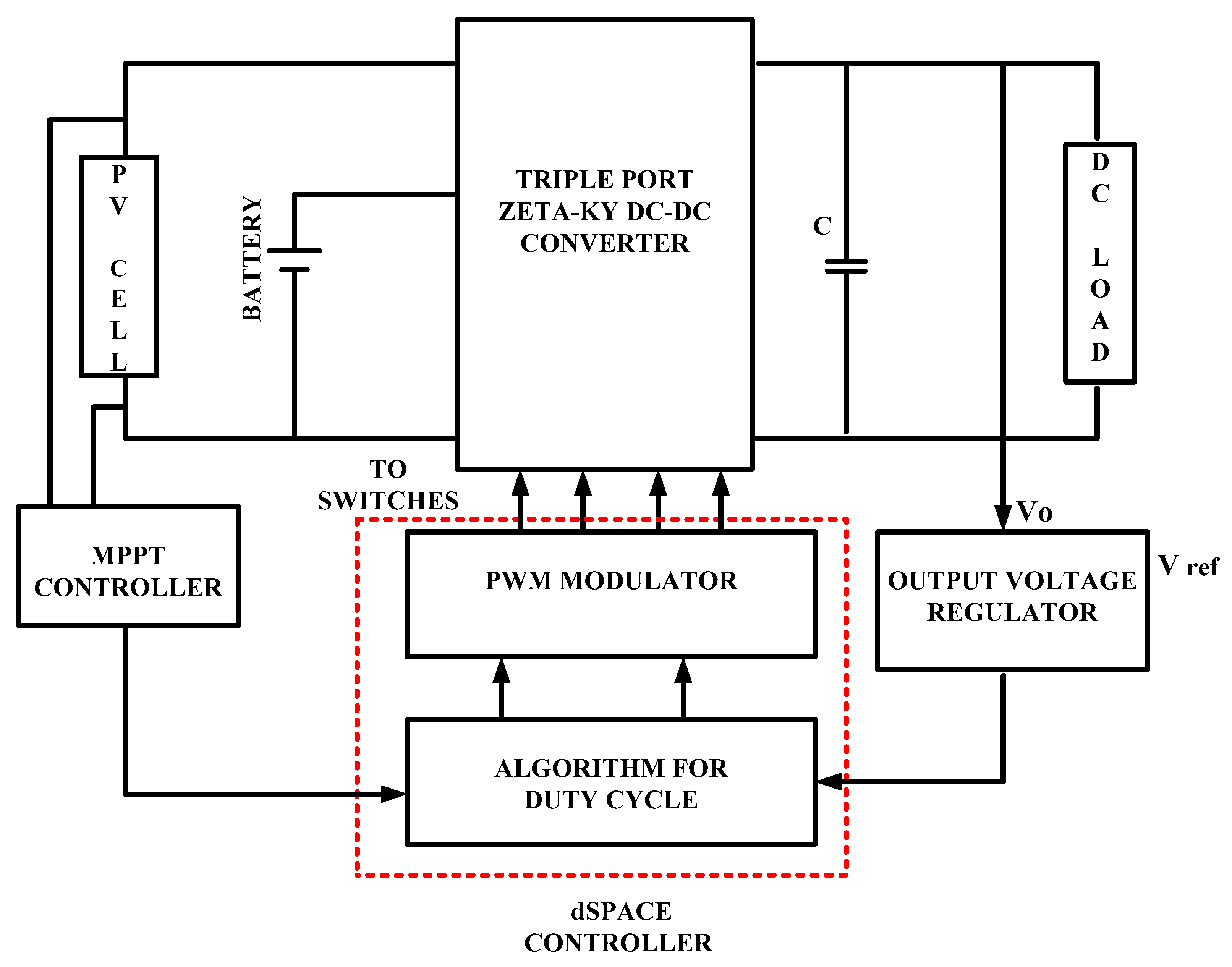
The proposed triple-port non-isolated Zeta KY converter is an integrated structure of a Zeta and a KY converter. The block diagram is shown in Figure 2. The circuit is fed with two inputs, one for the Zeta structure and other for the KY structure.
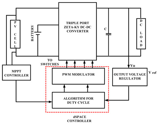
Figure 2.
Control architecture of the proposed triple port Zeta-KY converter.
The common elements of the conventional Zeta and KY converters are grouped to form a single output. The proposed converter with a novel structure has not been explored earlier. Thus, a dual input single output (DISO) structure has been designed for eliminating the use of isolation transformers. Since the Zeta and KY converters were integrated, the proposed triple port converter features the characteristics of both the structures. This proposed converter provides less output ripple voltage with high voltage gain and improved load transient response. The presented converter comprises three MOSFET switches S1, S2 and S3, three diodes D1, D2 and D3, three inductors L1, L2 and L3 and three capacitors C1, C2 and C3. L1 and L2 are individual coupled inductors and L3 is a filter inductor. The converter is designed to be operated in continuous conduction mode.
It is necessary to measure voltages or currents when feedback controllers are employed. In this proposed work, the actual output voltage of the controller was taken from the output, compared with a reference voltage and an error voltage signal was generated. This error signal was then fed to the controller.
Some assumptions are considered for the performance of steady state analysis: (1) The semiconductor devices are considered as ideal. (2) The parasitic parameters are neglected. (3) The voltage across the capacitors is assumed to be constant. For the purpose of analysis in steady state, the semiconductor devices were considered as ideal. An ideal switch has zero resistance and zero voltage drop in ON state and infinite resistance and zero current in OFF state. Hence, the power loss should be zero in both ON and OFF states even though practically it is not the case.
2.2. Modes of Operation of the Zeta-KY Converter
The Zeta-KY converter can be operated in unidirectional and bidirectional topologies. When both sources are from renewable energy sources or from regulated voltage sources, the converter operates in unidirectional topology. The power flow is from source to the load. When one source is renewable and other source is a battery storage system, the converter operates in bidirectional topology. The power may flow from the load to the source in order to charge the battery.
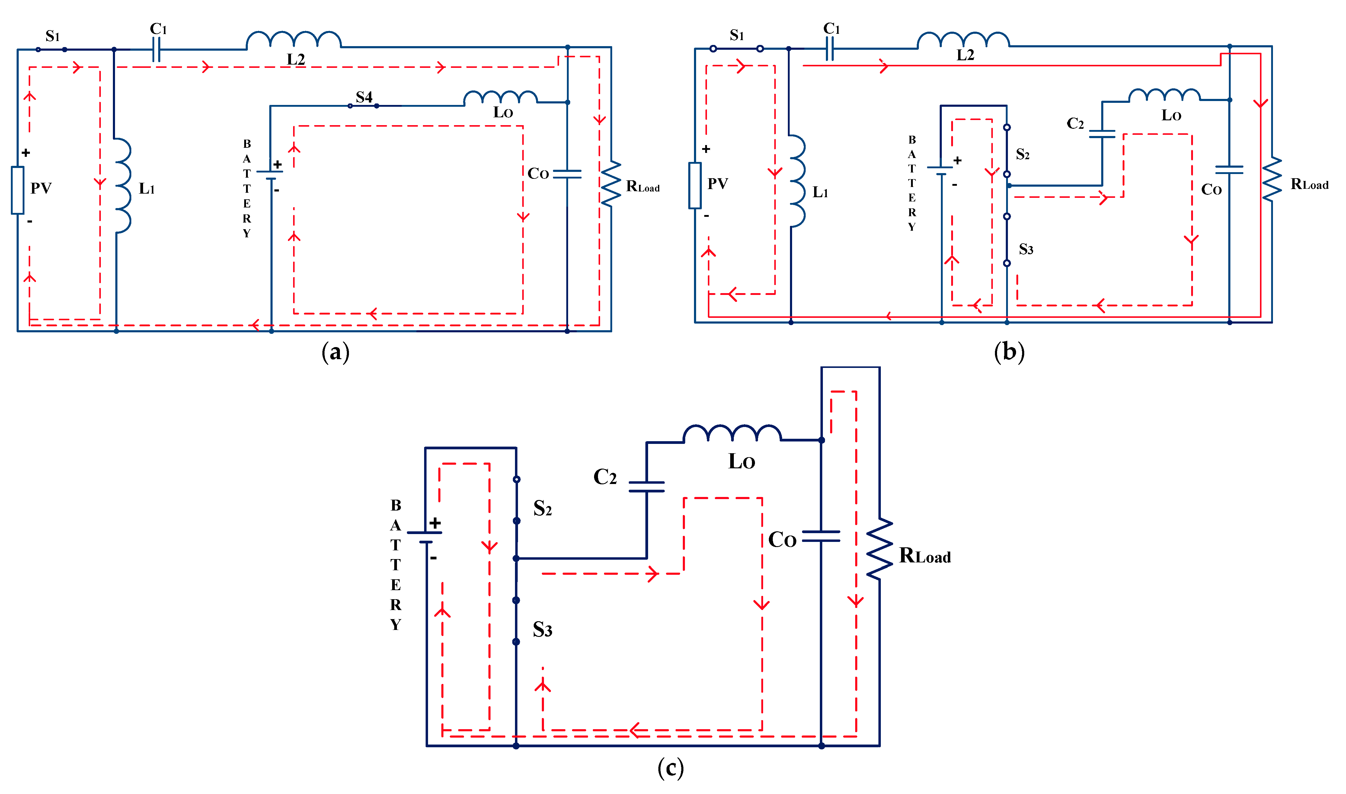
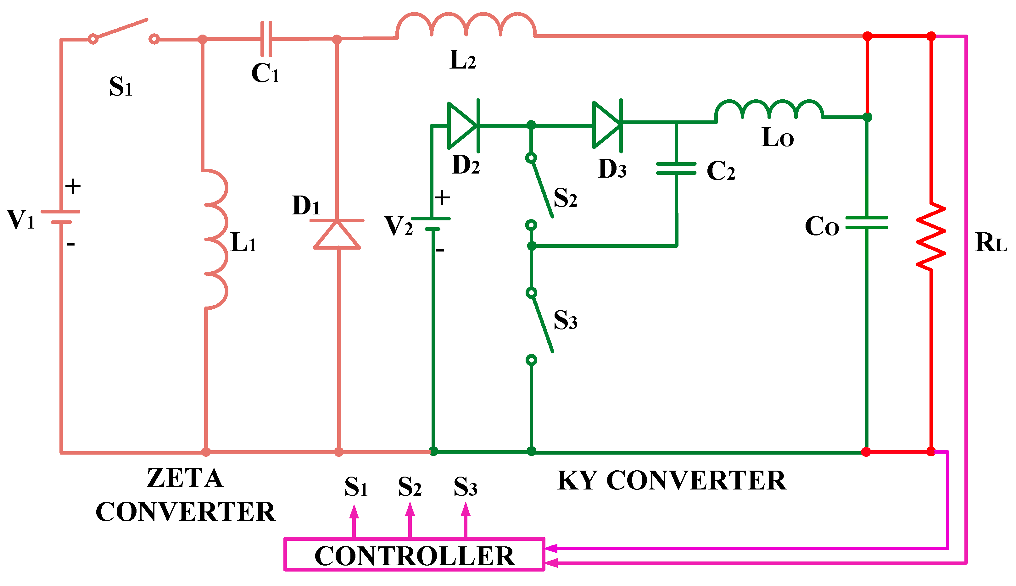
2.2.1. Topology 1: Unidirectional Converter
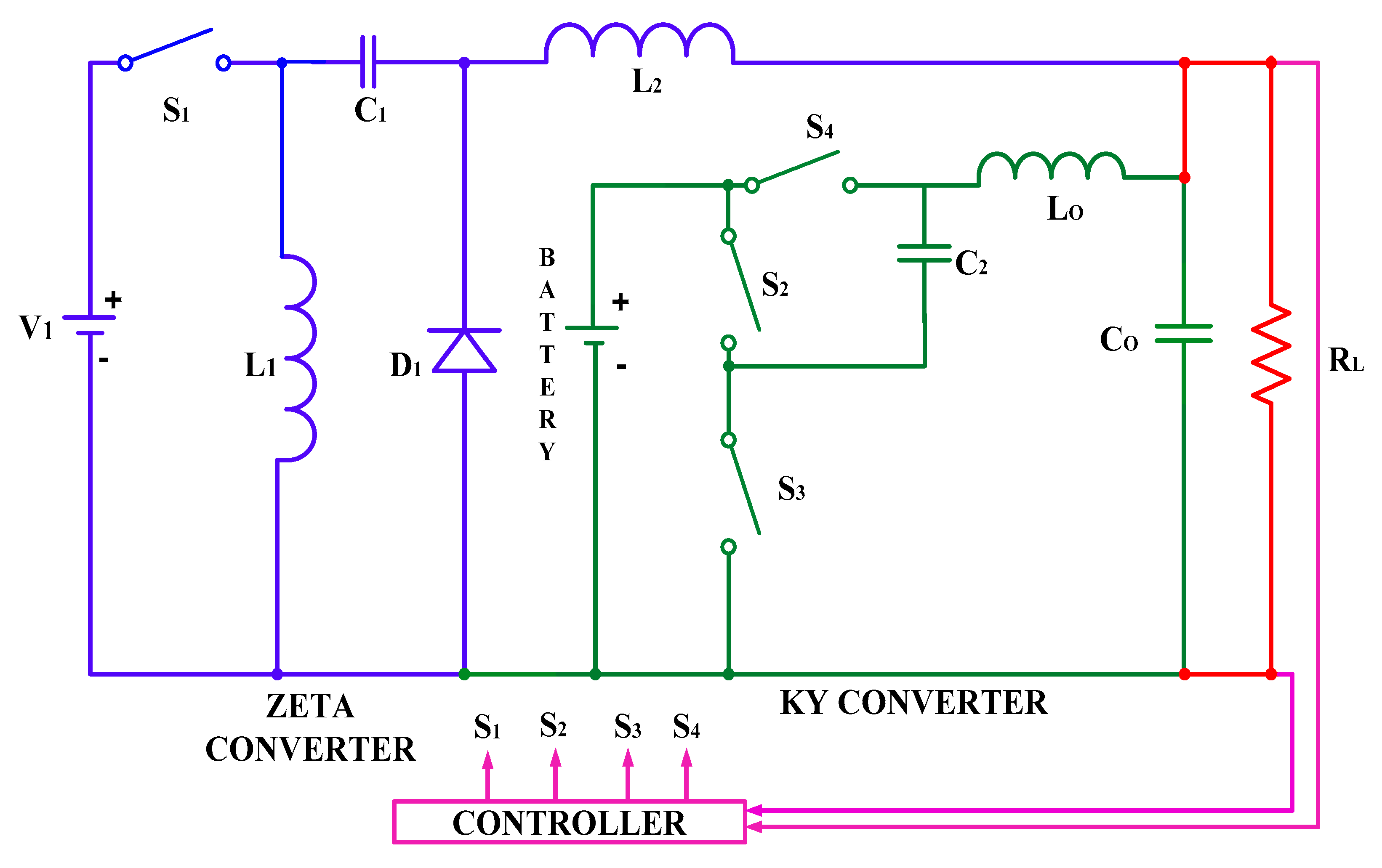
In this topology, both input sources were realized as dc voltage sources and the circuit were operated in different modes. Here, the power flow was from source to load. The duty cycles were fed appropriately to the switches so as to meet the load demand. The circuit diagram of the triple port Zeta-KY converter is shown in Figure 3. The conventional Zeta and KY converters are ported together and a modified triple port Zeta-KY dc-dc converter has been designed and developed. The parallel input parallel output (PIPO) architecture of multi porting was adopted. A multiport converter is basically designed by either connecting two or more converters in series or in parallel. It depends on the number of inputs and the number of loads connected to the multiport converter. In the proposed topology, two converters namely Zeta and KY converters were integrated in parallel, and the common elements were shared by both converters. By doing so, an inductor and a capacitor were eliminated from the basic configuration, hence reducing the size of the multiport converter.
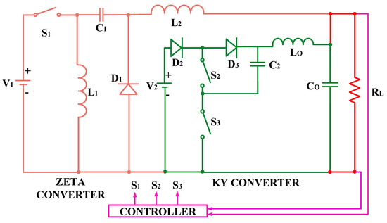
Figure 3.
Modified three port Zeta-KY dc-dc unidirectional converter.
The violet arrow referred to the feedback signal taken from the output voltage of the multiport converter and compared with a reference voltage set in the controller. This was a measure of voltage for unidirectional topology.
The operation of the converter is implicit through key waveforms for Topology 1 as shown in Figure 4. The variations of voltage and current through components in the MPC under different operating modes are depicted. The converter was operated in a continuous conduction mode (CCM). The inductors L1 and L2, capacitor C1 along with the switch S1 belonged to the Zeta part of the circuit. The switches S2 and S3, capacitor C2 and diodes D2 and D3 belonged to the KY part of the circuit. The diodes D2 and D3 were provided to avoid reversal of current towards the source V2. The diode D1 was provided for the purpose of freewheeling. The inductor L0 and capacitor C0 were filtering elements common for both the Zeta and KY converters. Both converters shared a common load. The operation of the converter has been explained through different modes.
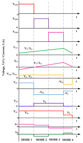
Figure 4.
Key waveforms of the proposed converter.
- (i)
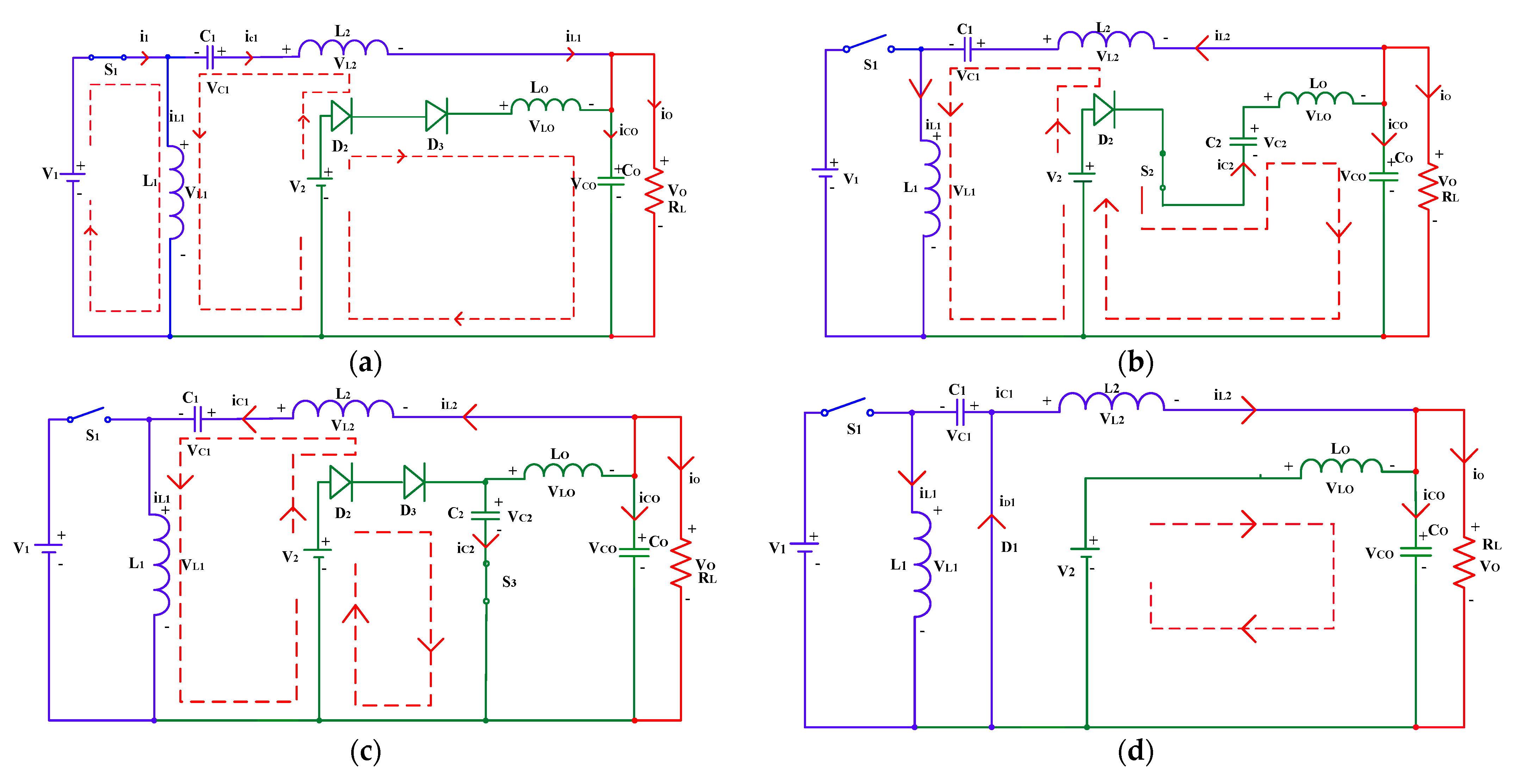
- Mode 1 (S1 is ON and S2, S3 are OFF): In this mode, the switch S1 is turned on and switches S2 and S3 were turned off. Both the sources V1 and V2 were supplying the multiport converter. The inductors L1 and L2 were charged to the value of input voltage V1. The current through L1 increased linearly to a value V1/L1. The capacitor C1 was charged equal to Vo, which was the output voltage of the converter. Diode D1 was reverse biased and diodes D2 and D3 were forward biased.
The converter was analyzed in a steady state condition and the corresponding equations have been obtained.
- (ii)
- Mode 2 (S2 is ON and S1, S3 are OFF): In Mode 2, the switch S2 was turned on and switches S1 and S3 were turned off. V1 was therefore not supplying the circuit. The source V2 supplied the load through D2 and D3. The inductor L1 discharged its magnetic energy and reduced the voltage across it. The positive voltage of V2 turned on switch S2 and the input current flowed through S2, capacitor C2 and to load through L0. Capacitor C2 discharged. In addition, L2 then discharged to a value equal to the output voltage.
- (iii)
- Mode 3 (S3 is ON and S1, S2 are OFF): The switches S1 and S2 were turned off in this mode. Switch S3 was turned on. C2 started charging and the voltage across it was equal to V2. The source V2 supplied the load through C2 and LO.
The circuit diagrams under different operating modes in unidirectional topology configurations are shown in Figure 5.
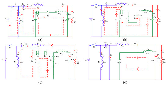
Figure 5.
Equivalent circuits of the proposed multiport converter with current directions: (a) Mode 1; (b) Mode 2; (c) Mode 3; and (d) Mode 4.
- (iv)
- Mode 4 (S1, S2, S3 are OFF): This is the mode in which all the switches were open. The current i2 flowed through the inductor L0. The diode D1 freewheels through the inductor L2 when there is no source voltage. The energy stored in the inductors dissipated when all switches are turned off. Thus, in turn diode D1 was forward biases.
2.2.2. Topology 2: Bidirectional Mode
Renewable energy applications have now become very vital in the field of energy generation. Of the whole of the renewable energy sources, solar energy is the most readily and easily available source for utilization. Hence, to effectively make use of the solar energy, the proposed multiport converter has been integrated with PV module. This triple port dc-dc converter was operated with one source as PV and other source as battery. Since the battery was used, a bidirectional power flow was possible in this topology.
The circuit was constructed in such a way that a renewable source such as PV fed the load through the Zeta converter. The other source was a battery that connected the load through the KY converter. Both the sources shared a common load, thus acting as a dual input single ended output (DISO) converter. The PV output voltage depended on the irradiance of the solar energy. The maximum power point tracking (MPPT) algorithm was implemented in the controller connected to the PV panel. The MPPT—fractional open circuit voltage was the principle of tracking maximum available power from the PV module, by operating with the maximum efficient voltage. The MPPT algorithm was applied to the circuit based on the design specifications of the PV. The circuit diagram for the bidirectional topology is shown in Figure 6. The violet arrow was again the measure of the output voltage which was fed back to the controller for bidirectional topology.
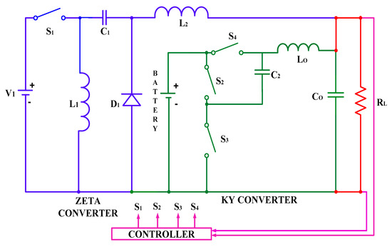
Figure 6.
Proposed modified three-port Zeta-KY dc-dc bidirectional converter.
The diodes D2 and D3 connected in the circuit of Topology 1 (unidirectional) were eliminated in the circuit of Topology 2 (bidirectional). This was implemented to provide a bidirectional power flow i.e., the power flow from the battery source to the load and from the load to the battery for charging the battery. The bidirectional power flow was implemented in this topology to charge the battery through the KY converter itself. Switch S4 was connected in such a way that it was suitably turned on to allow power flow from the load to the source. CCM of operation was also performed in this topology. The operation of the MPC is explained in Figure 7 through variations in the power of PV panel (PPV), battery (Pbattery) and load (PLOAD).
- (i)
- Case 1—presence of high irradiation (PPV > PLOAD): The PV panel fed the load through the Zeta converter. Switch S1 was turned on. In this case, the converter operated as single input single output (SISO) converter. The excess power that was not consumed by the load was utilized for charging the battery through turning on switch S4 from the load bus. The converter acts in bidirectional mode as shown in Figure 7a. Hence, energy conservation is carried out in this case.
- (ii)
- Case 2—presence of moderate irradiation (PPV < PLOAD): When the PV was not able to completely meet the load demand, the battery energy storage system supported it through the KY converter. Now, switches S1, S2, S3 were turned on sequentially. In this case, the converter operated as dual input single output (DISO) converter as shown in Figure 7b.
- (iii)
- Case 3—absence of irradiation (PPV = 0): The battery fed the load through the KY converter. Switches S2 and S3 were turned on as in Figure 7c and the converter operated as single input, single output (SISO) converter.
Figure 7.
(a) Case 1: PPV > PLOAD; (b) Case 2: PPV < PLOAD; (c) Case 3: PPV = 0 (when there is no irradiation).
Figure 7.
(a) Case 1: PPV > PLOAD; (b) Case 2: PPV < PLOAD; (c) Case 3: PPV = 0 (when there is no irradiation).
Therefore, the converter fed with PV and Battery as the input sources, acted in both unidirectional and bidirectional modes and the feature of the proposed modified triple port converter was that the converter might be operated in SISO and DISO modes according to the load demand by making the optimum use of power. Energy management was carried out well in the proposed multiport converter. The attributes of the novel combination of Zeta and KY converter has been explicitly brought out well.
The PV panel output varies in accordance with irradiance. The MPPT control algorithm (Appendix A.4) is implemented in the MPC to maintain a constant output voltage from maximum power point tracking. PI Controller is used to control the switches in the multiport converter. The MOSFET switches S1, S2, S3 and S4 are operated with a switching frequency of 25 kHz. The actual output voltage of the converter is fed to the controller and is actuated in the PI controller. Thus, a closed loop controller is implemented in the converter. The operating mode of the converter is decided according to the load. The transfer function of the converter plant is determined for PV mode and battery mode.
The proposed multiport converter has two input sources, V1 (PV) and V2 (battery). When S1 is open, the first input source V1 will not be able to feed the load. However, the second source V2 will be supplying the load. By suitably turning on the switches S2, S3 and S4, it is possible to feed the load power continuously, even if S1 is off. This is the advantage of the proposed topology in which if one of the sources is not supplying the load, the other source will supply the load.
3. Analysis and Design of the Proposed Zeta-Ky Converter
The proposed DISO converter has been analyzed to obtain the design values of the components used in the MPC. From the steady state equations obtained from different operating modes of the converter, several current and voltage equations have been acquired.
3.1. Output Voltage of the MPC
The output voltage equation is derived by applying volt-sec balance on the inductance L2 used in the multiport converter. Combining Equations (1), (4), (7), and (10), the average voltage across the inductor is:
where are duty cycles for switches V1 and V2 are the input voltage sources. VC1 and VC2 are the voltages at C1 and C2, respectively.VL1, VL2 and VLO are the voltages across inductors L1, L2 and LO, respectively.
Solving the above equations, the output voltage of the three-port converter is given by:
3.2. Power Devices Voltage
The voltage at switches and diodes are obtained by applying Kirchhoff’s voltage law, (KVL) to the multiport converter when operated at different modes.
where are the voltage stress across the MOSFET switches , respectively. Voltage stress across the diodes are given by respectively:
3.3. Inductor Currents
Applying the charge-sec balance technique, the current through the inductors is expressed as:
where are the currents through the inductor , respectively.
3.4. Voltage and Current Ripples
By employing small ripple approximation techniques, the values of inductors and capacitors have been calculated. Voltage ripple are given by and current ripples by .
3.5. Passive Components Selection
Size calculation for is given by:
where denote the ripple current for inductors and fs is the switching frequency of the proposed converter. To calculate inductors size, is generally assumed to be in the range of 10% to 20% of full load. Similarly, the capacitors size is chosen according to the maximum ripple voltage allowed at the capacitors. Size calculation for each capacitor is expressed as:
where represent the ripple voltage at the capacitor C1, C2 and C3 and i1, i2 and i0 denote the currents related with the PV power source, energy storage battery and load consumption, respectively. The calculated values for inductors L1, L2 and LO are 0.62836 mH, 0.72361 mH and 0.517122 mH, respectively. The calculated values of capacitors C1, C2 and CO are 0.12860 mF, 0.381944 mF and 0.10706 mF, respectively.
The transfer functions of the modified triple port converter have been obtained for PV and battery modes.
The transfer function of the converter during PV mode is shown as below:
The transfer function of the converter during battery mode is as below.
The circuit was analyzed, and the parametric values were determined for the proposed modified triple port the Zeta-KY converter. Table 1 shows the design specifications for the PV and battery sources. The ratings of the components’ input and output voltage ripples were calculated.

Table 1.
Design specifications for the proposed MPC.
4. Results and Discussions
4.1. Simulation Results
The converter was simulated in MATLAB platform using the parameters set depicted in Table 1. The converter is operated in open loop control. The actual output voltages of the MPC are compared with the estimated output voltage. Table 2 depicts a comparison between the estimated and output voltages obtained by varying duty cycles and constant input voltages.
Table 2.
Comparison table for the output voltage with varied duty cycles in unidirectional mode.
The source voltages V1 and V2 were varied and the output voltage was estimated by maintaining constant duty cycles for the switches. These estimated output voltages were compared with the actual output voltages as shown in Table 3. In both tables, the actual voltages obtained from simulation were approximately closer to the estimated output voltages. Thus, the operation of the unidirectional modified triple port Zeta-KY MPC was elucidated, and the calculated and actual output voltages are compared.
Table 3.
Comparison table for the output voltage with fixed duty cycles in unidirectional mode.
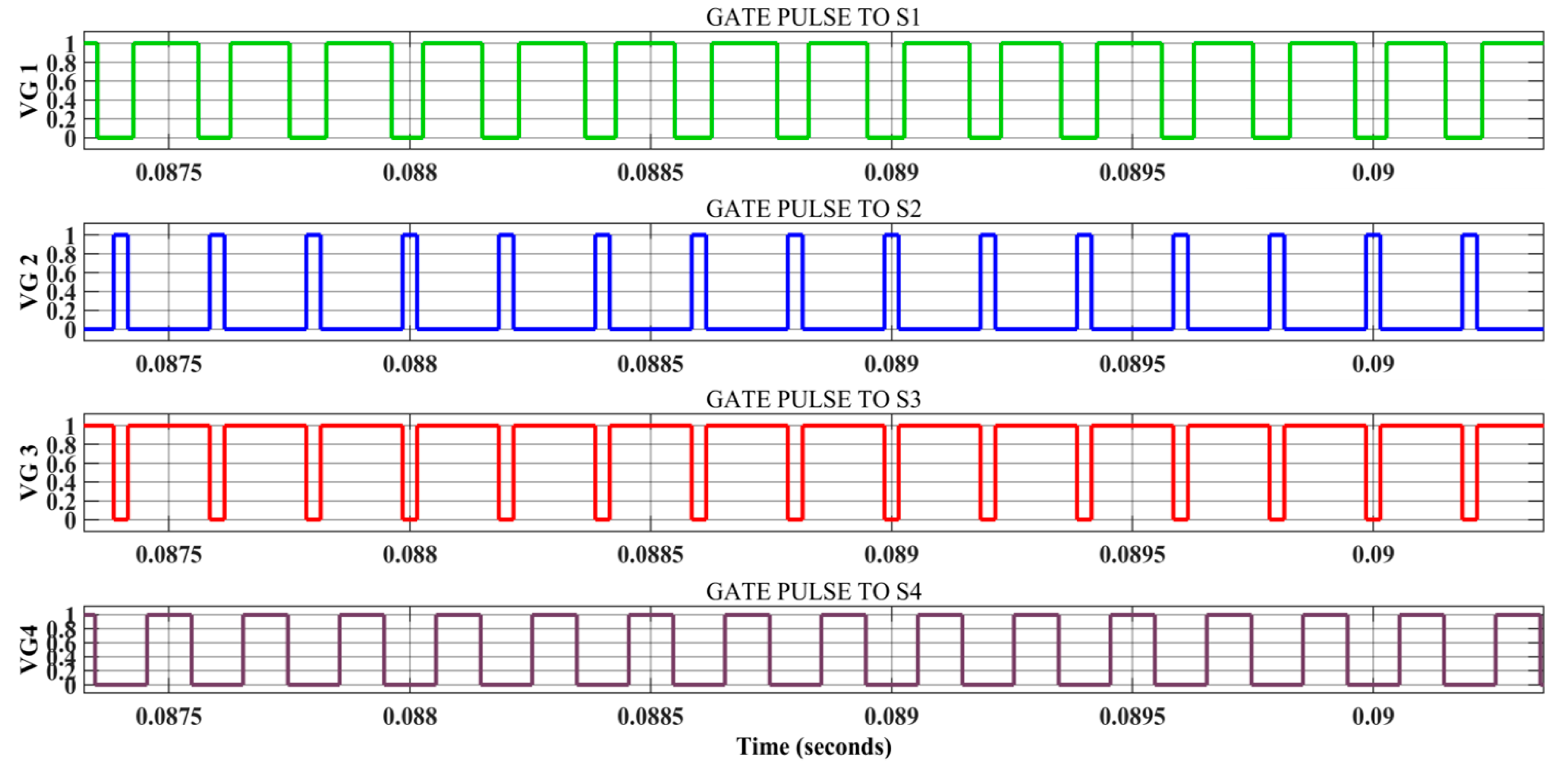
Figure 8 shows the gate pulses generated from the controller to turn-on the MOSFET switches S1, S2, S3 and S4. The pulses are generated by the controller that is continuously tracking the output voltage, comparing it with the reference voltage and thereby generate pulses according to the operating mode. The proportional gain for the PI controller, KP = 100 and integral gain, KI = 0.1 have been considered. These values have been obtained by tuning the PI controller in MATLAB.
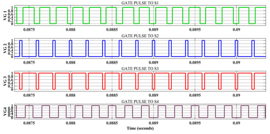
Figure 8.
Pulses generated for switches S1, S2, S3 and S4 (bidirectional).
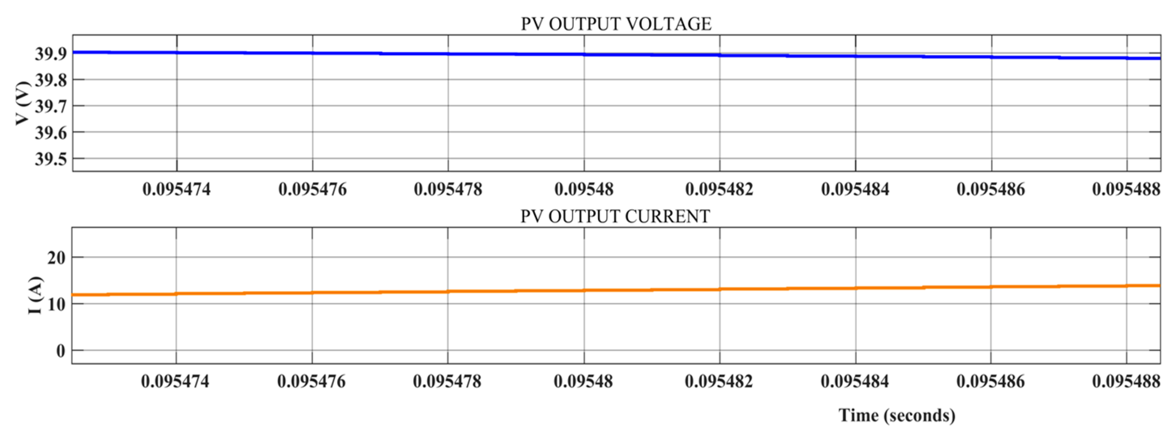
The PV fed the converter when there is solar irradiance. Applying MPPT controller to the PV panel, 40 V output voltage is constantly maintained, which fed the load through the Zeta converter. This was facilitated by triggering switch S1. Figure 9 shows the output voltage and current fed from the PV at a constant irradiance. At a particular irradiance, the output current of PV will be constant only. This current will change only when the irradiance will change.
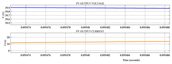
Figure 9.
Output voltage and current from the PV to feed the converter.
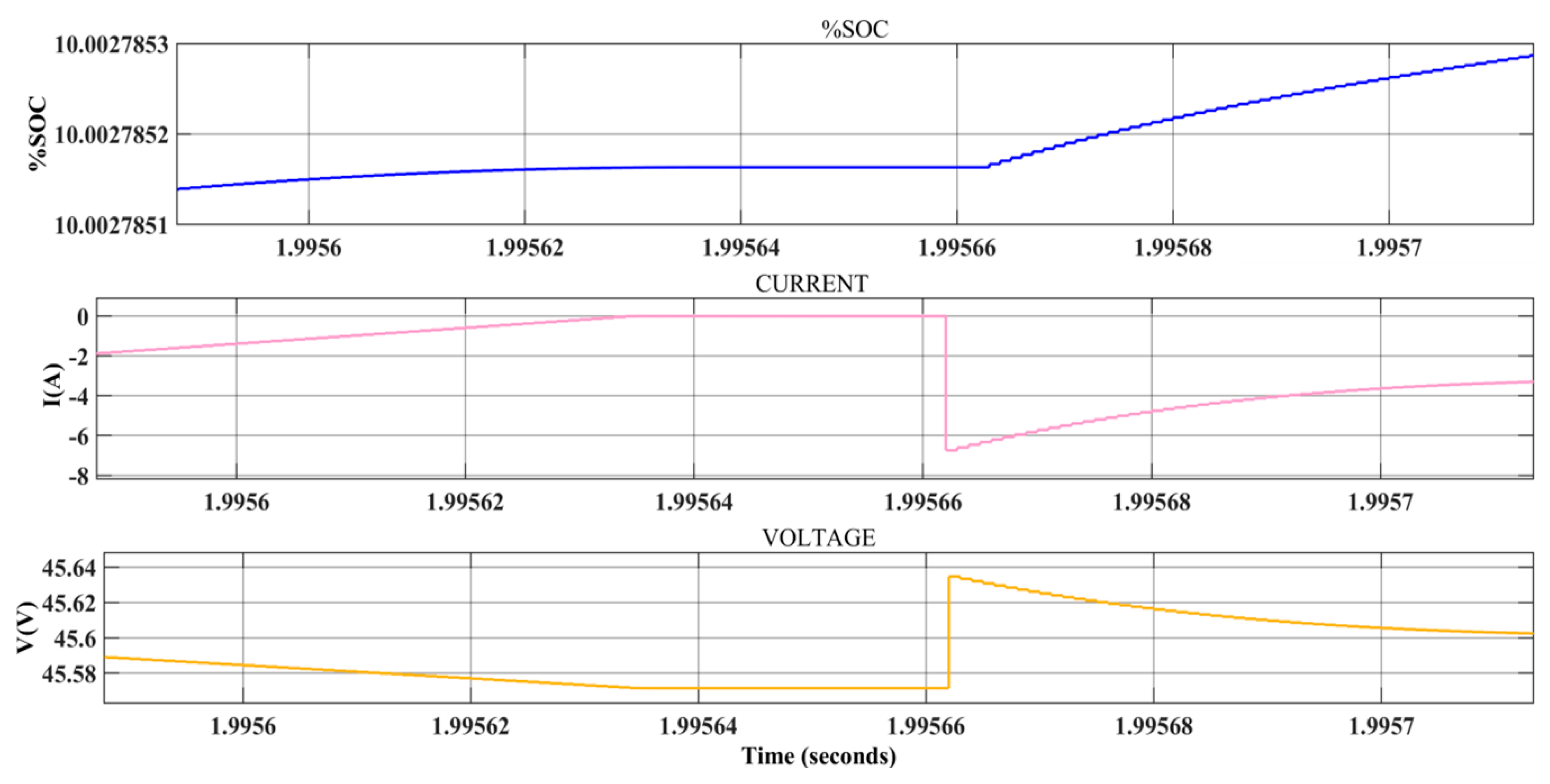
The battery was charged during bidirectional mode through the switch S4. Figure 10 shows battery state of charge (SOC), with a battery voltage of 45 V and a current of −2 A in bidirectional mode. It should be noted that since the SOC of battery changes, the battery current falls immediately and again increases within a very shorter time.
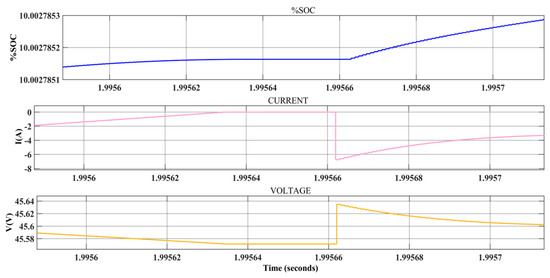
Figure 10.
Battery waveforms: state of charge (SOC), voltage and current.
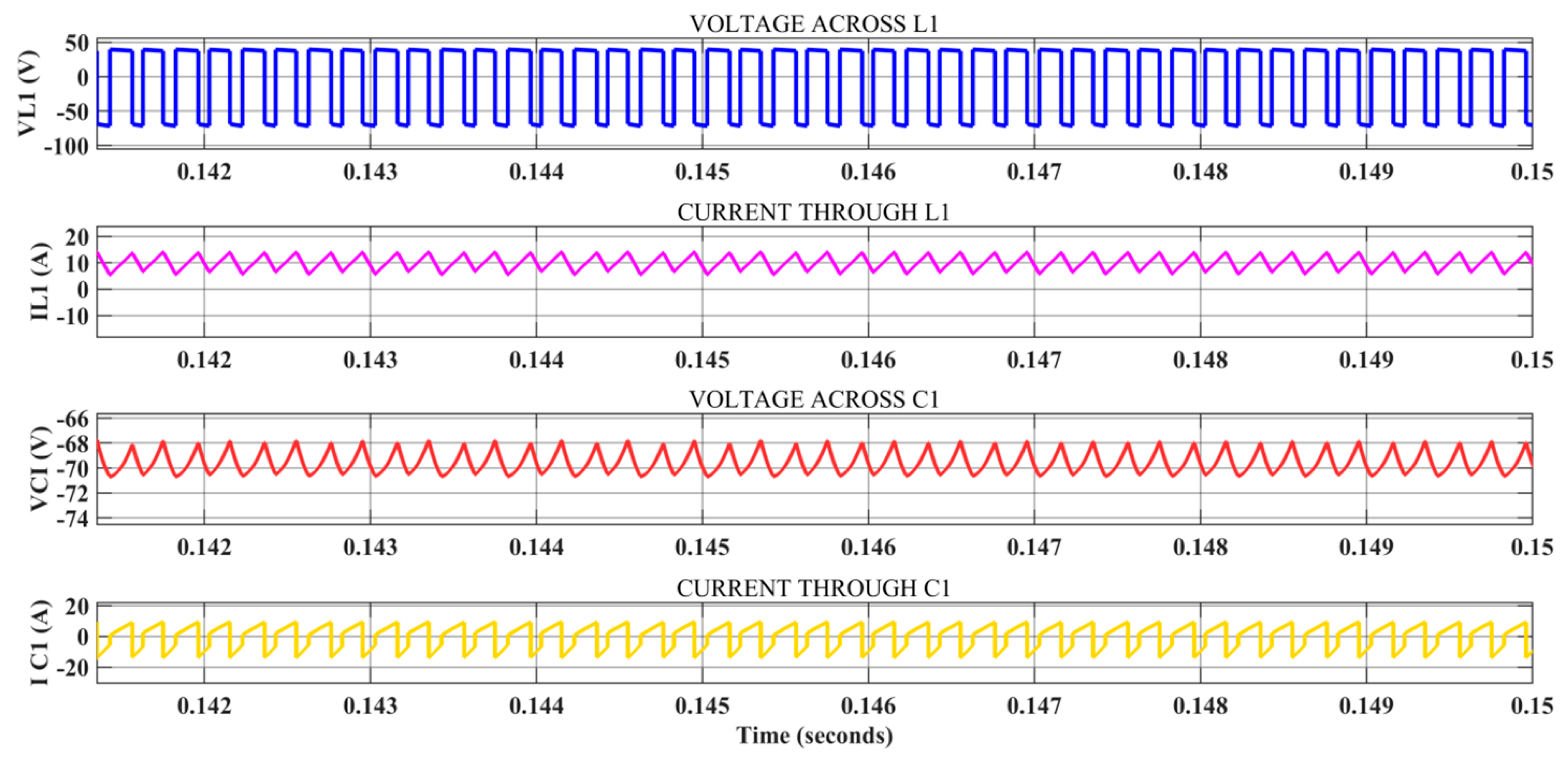
When the PV source is connected to the Zeta part of the MPC with a load connected to the output, the inductor L1 is initially charged to a value equal to the input voltage of the PV with 40 V. Later it discharged to −40 V. With the MPC working in continuous conduction mode, the current through the inductor L1 is continuous as shown in Figure 11.
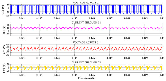
Figure 11.
Waveforms of voltage across L1, C1 and current through L1, and C1.
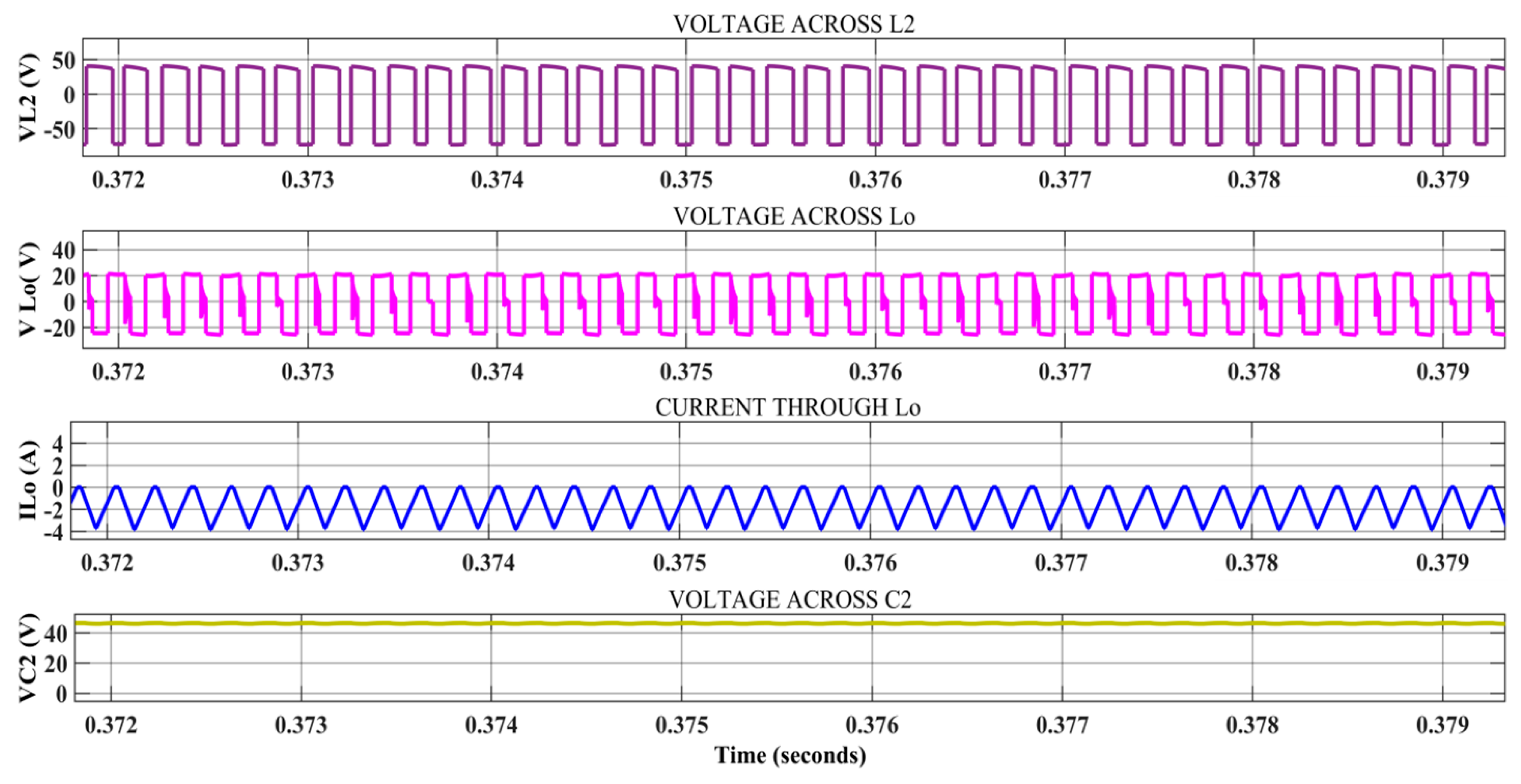
Figure 12 shows the simulated waveforms of the voltage and current through other inductors L2, L0 and C2. The CCM mode was demonstrated from the waveform shown by the current through the inductor L0.
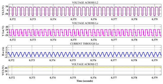
Figure 12.
Waveforms of voltage across L2, L0, C2 and current through L0.
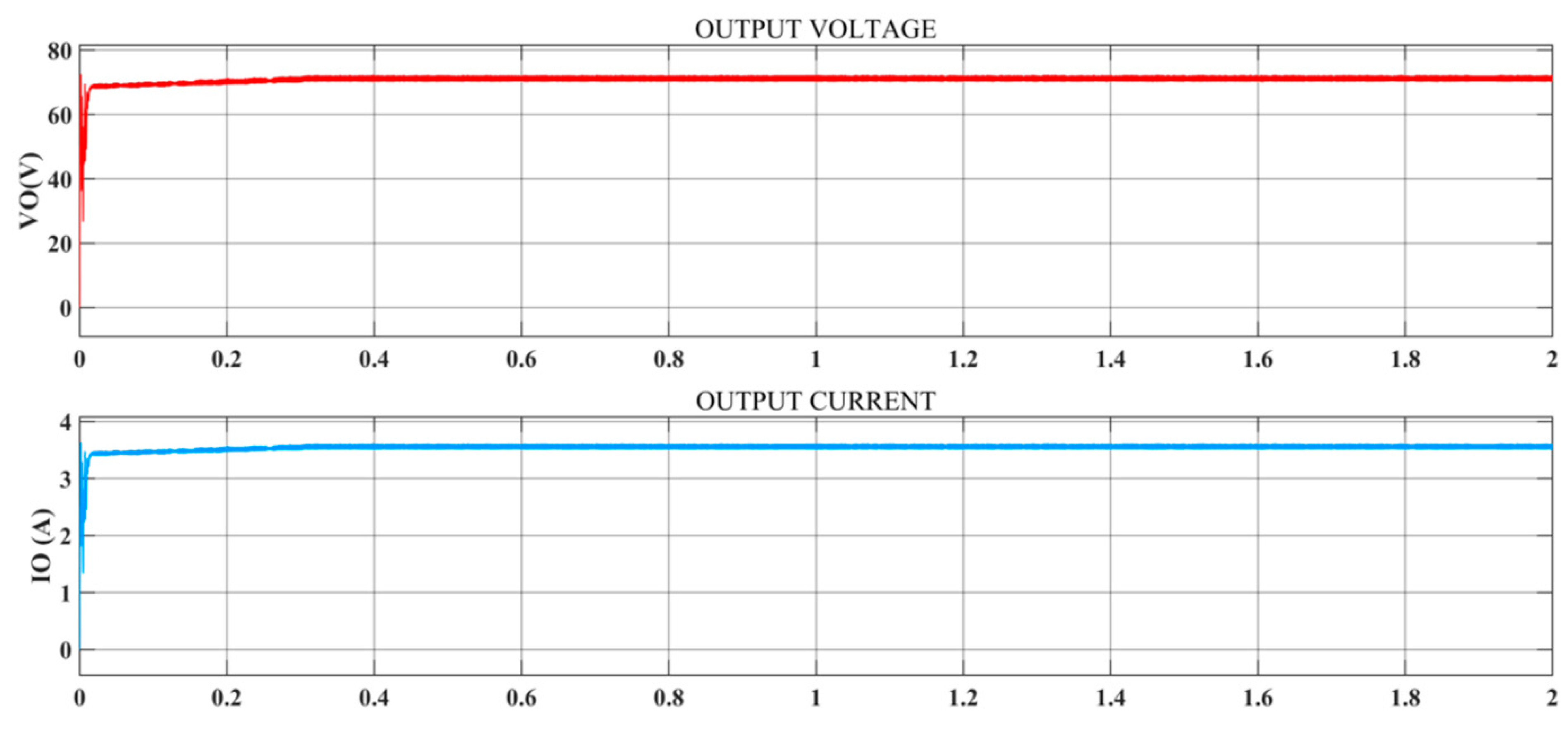
For the specified design of the proposed converter, the output voltage and current waveforms obtained through the simulation are shown in Figure 13. A constant output voltage of 70 V was obtained across the 20 Ω resistive load.
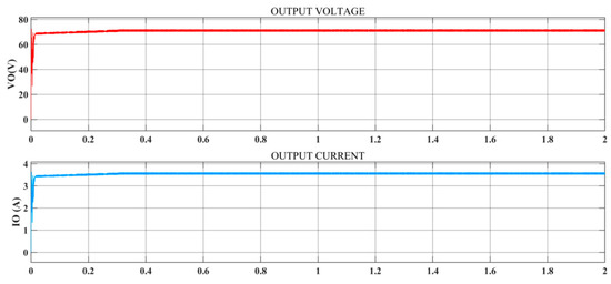
Figure 13.
Output voltage and current waveforms of the proposed MPC.
4.2. Experimental Results
The simulation results were verified through a real time hardware set up of the converter. The MPPT algorithm (Appendix A.4) was implemented for maintaining constant voltage by tracking maximum power from the PV. The components used in the hardware set up and their calculated individual losses have been listed in Table 4.
Table 4.
Calculation of efficiency of the converter through different losses.
The pulses were generated with a Dspace1103 controller with the hardware converter. Figure 14 depicts the real time hardware set up of the proposed triple-port Zeta-KY converter. A load resistor of 50 Ω was connected and the output was verified for different loads.
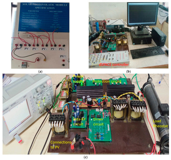
Figure 14.
(a) PV panel of 250 W; (b) experimental set-up of the proposed converter with dSPACE controller; and (c) closer view of the converter.
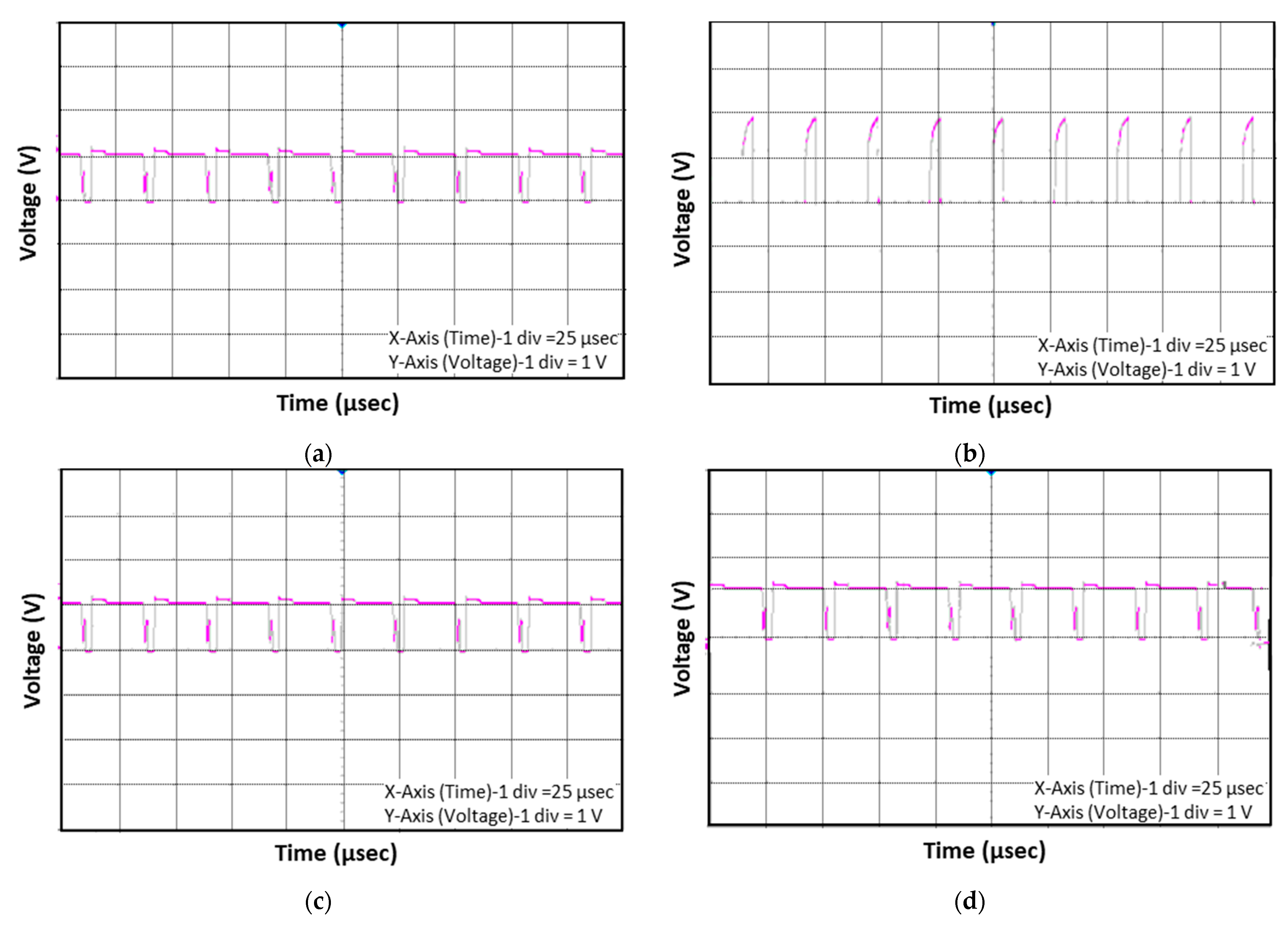
The dSPACE controller generated pulses to trigger switches S1, S2, S3, S4. The generated pulses from the controller were observed through the digital storage oscilloscope (DSO). The pulses generated for all MOSFETs shown in Figure 15 are similar to the simulated waveforms of the converter.
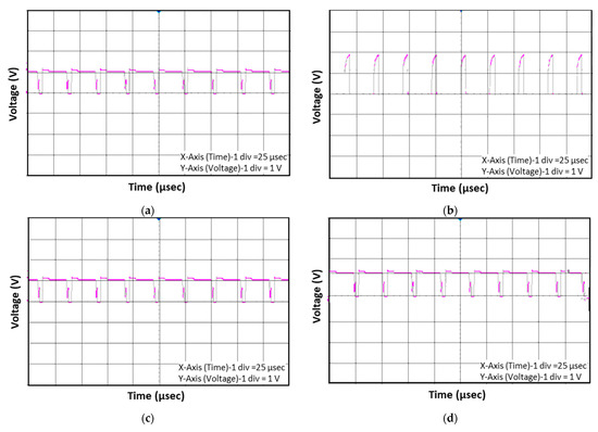
Figure 15.
Pulse generated for (a) Switch S1; (b) Switch S2; (c) Switch S3; and (d) Switch S4.
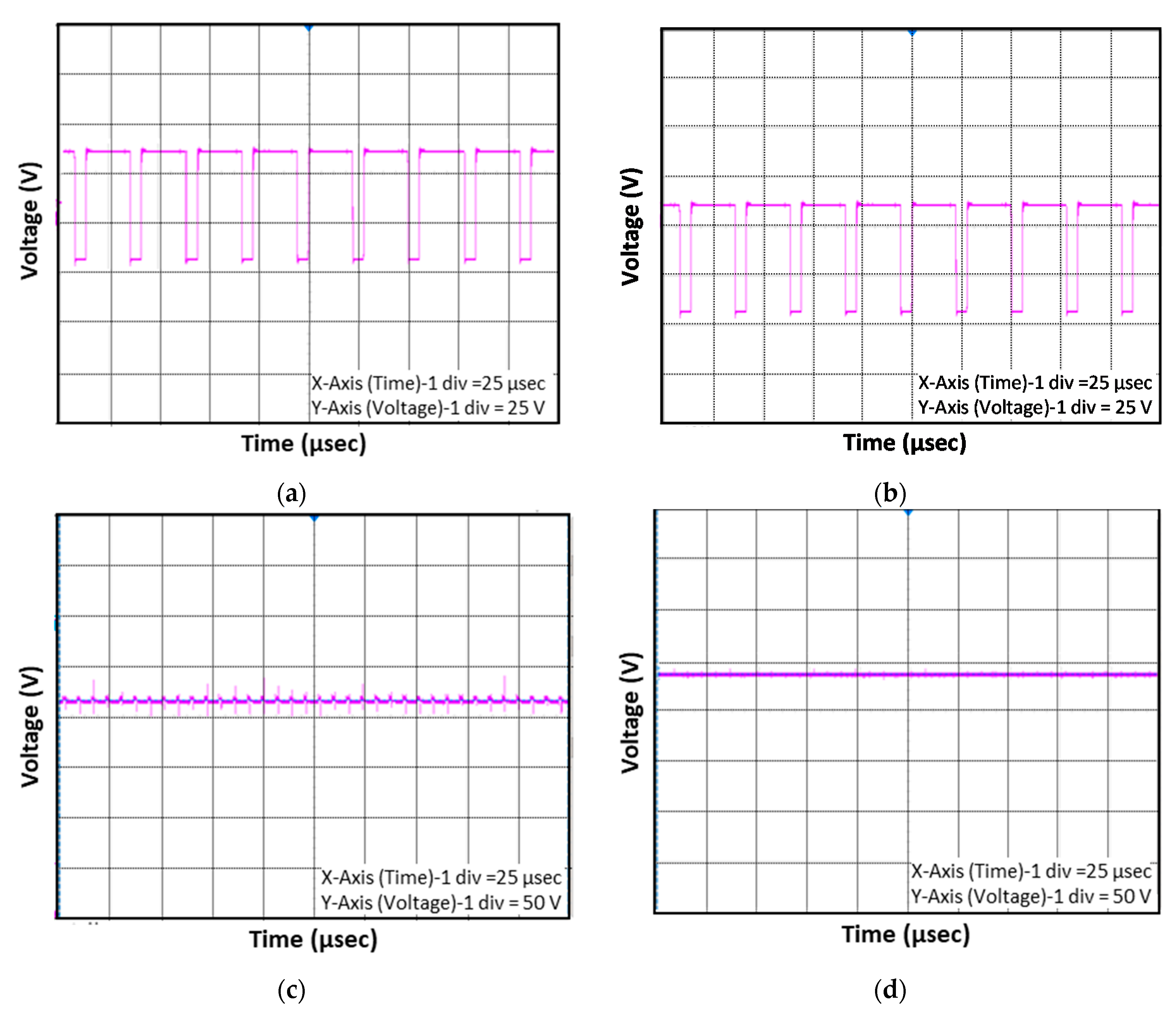
The switches were operated at a switching frequency of 25 kHz. The voltage across the inductors L1 and L2 are shown in Figure 16a,b, in which the plot is obtained for a scale of 25 V/div. The inductor L1 charged and discharged to its input voltage from the PV source of 40 V. The voltage across the capacitor C1 initially charged to a value equal to the input voltage and discharged to maintain a constant output voltage, thus maintaining at −70 V as shown in Figure 16c. Figure 16d shows that capacitor C2 charged to a voltage equal to the battery voltage of 40 V, since C2 was connected to the KY part of the MPC in which battery acted as the input source.
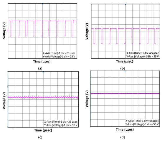
Figure 16.
(a) Voltage across L1; (b) voltage across L2; (c) voltage across C1; (d) voltage across C2.
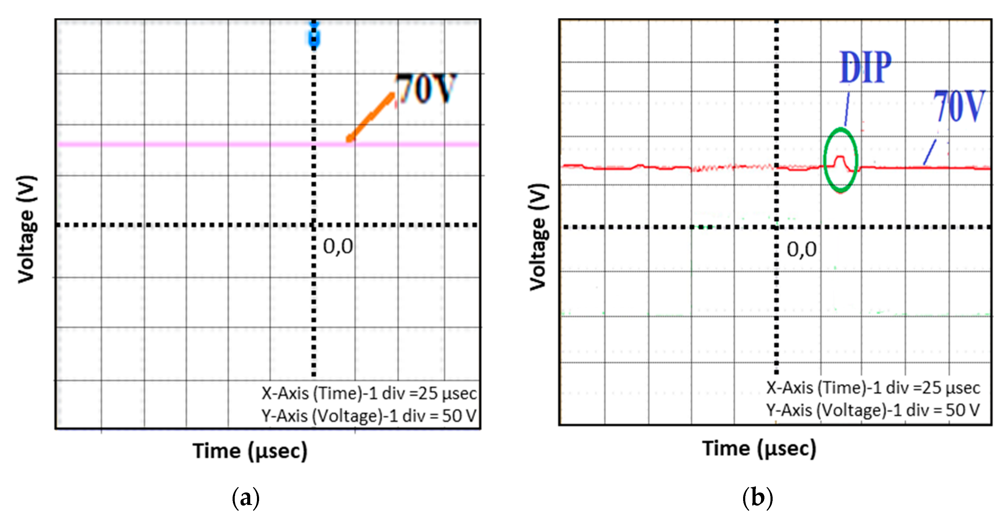
The output voltage of the proposed converter was maintained with a constant output voltage of 70 V in the dc grid. The output was observed for a constant load of 20 Ω as shown in Figure 17a. This resistive load of 20 Ω was varied to 30 Ω and the output was observed as shown in Figure 17b. The output voltage was 70 V at 20 Ω load and at 30 Ω, there was a small dip in voltage and the output voltage was maintained constant again at 70 V. This demonstrated that the proposed triple-port converter maintained constant output voltage that could be fed to the dc grid for further applications. Thus, the converter is maintaining the constant output voltage irrespective of load changes. One of the characteristic features of the KY converter was demonstrated here with good load transient response.
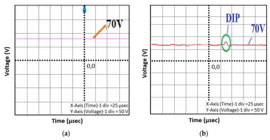
Figure 17.
Constant output voltage of the MPC (a) with constant resistive load of 20 Ω; (b) with dynamic loads (varied from 20 Ω to 30 Ω).
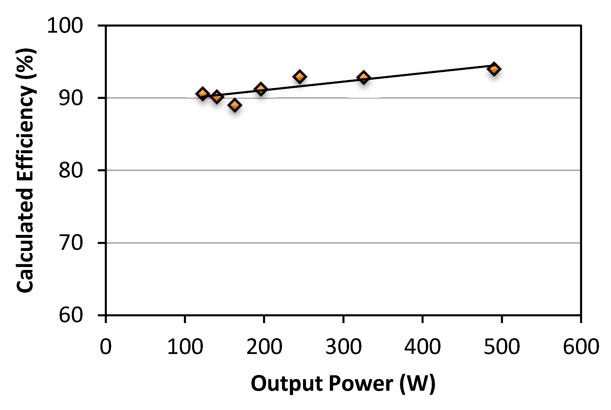
The output load resistance was varied from 10 Ω to 50 Ω and hence variable output power was obtained. The calculated efficiency curve has been plotted with respect to output power in Figure 18. The converter showed a maximum of 94% at 500 W. The graph is plotted by varying the resistive load gradually from 10 Ω to 50 Ω in bidirectional mode. At 30 Ω resistance when the PV was delivering 286.8 W, the battery charged itself drawing 104 W power. The total input power fed into the converter was 182.8 W. At this instant, there was a small dip in the calculated efficiency at 162.77 W output power. The complete calculations of power loss and efficiency have been shown in Appendix A.1 and Appendix A.2 respectively.
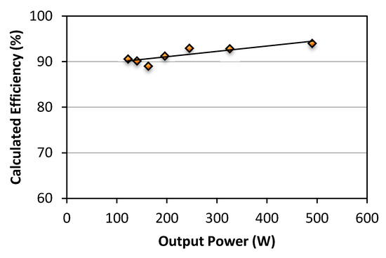
Figure 18.
Calculated efficiency curve for the converter at variable loads.
4.3. Comparative Analysis
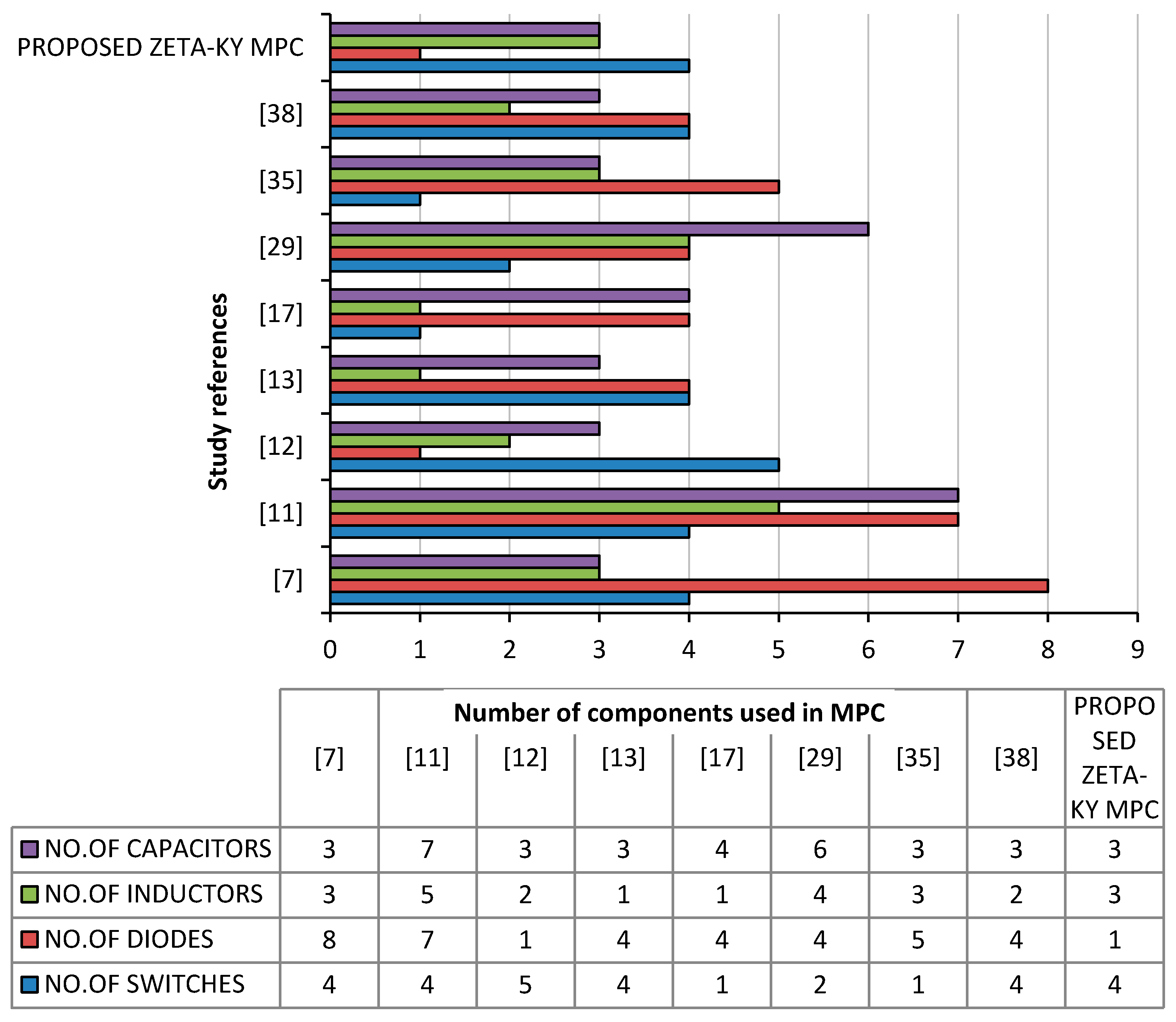
The number of components used in the converter plays a vital role in the performance and calculated efficiency of the converter. The stress and the losses encountered on each component is very imperative. Hence, the number of components employed in the proposed triple-port modified Zeta-KY converter was compared with those of the conventional multiport converters. In comparison, the proposed converter had moderately lesser number of components with converters of the same power ratings as shown in Figure 19.
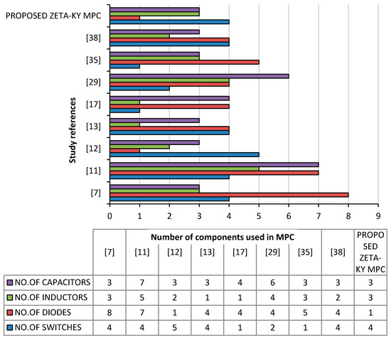
Figure 19.
Comparison of conventional multiport converters with the proposed modified triple port converter on the basis of components employed.
Multiport converters are known for combining one or more converters to optimize the renewable power sources in an effective way. The blend of two or more converters effectively reduces the number of active and passive components thereby increasing the calculated efficiency and minimizing the losses incurred. However, the reduction in number of switches is not the direct indication for reduction in size or cost. In practical cases, reduction of a switch not only reduces appreciable losses, but also the complexity related with the commutation process, design of driver units, etc., is reduced. In this work, two renewable sources or combination of one renewable energy source with battery energy sources enhanced the reduction of a switch and a pair of inductor and capacitor. If hybrid renewable energy sources are to be fed, then ‘n’ port MPC has to be designed in which cascading of ‘n’ dc-dc converters will considerably reduce additional switches and passive elements. Hence, the proposed MPC would be efficient for the rated load feasible for hybrid electric vehicles.
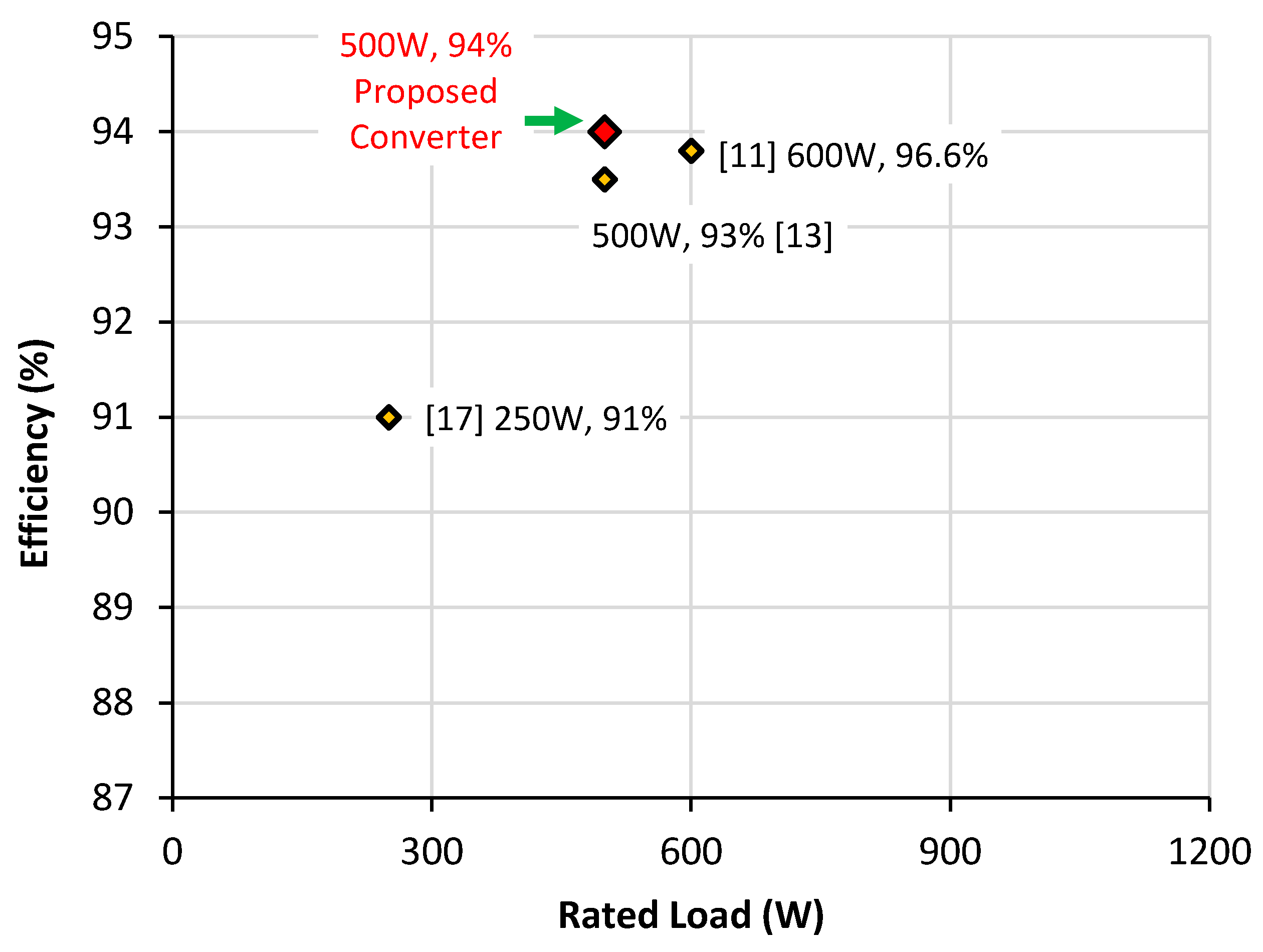
Figure 20 shows a comparison plot for the efficiencies of the conventional and the proposed MPC. The power converters considered for comparison were sampled here with their maximum rated load. The load and the corresponding efficiencies are shown for various multiport converters.
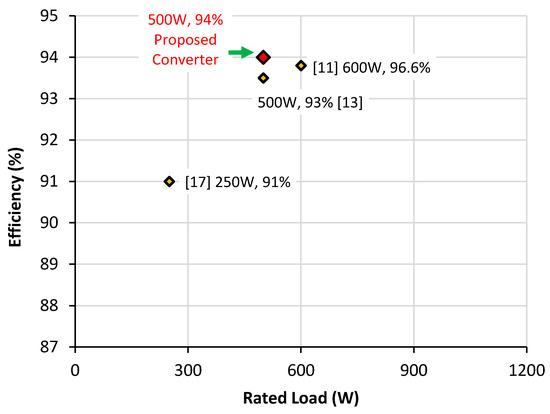
Figure 20.
Scatter plot between calculated efficiency and rated load for comparing the proposed and conventional MPCs.
From the plot, it could be inferred that at 500 W of rated power, the proposed converter produced the best calculated efficiency compared to the other reported values at different rated powers. The converter reported in [13] demonstrated efficiencies close to the current converter with similar rated power. Though the calculated efficiency reported in [11] was greater than the proposed converter here, it has the ability of supplying constant power to the load. All the input ports to the converters of [11,13] were fed from external sources. However, in the proposed modified Zeta-KY converter, one of the sources (battery) was charged by the converter itself through bidirectional charging. Furthermore, the control complexity and the inductive components used in these converters of [11,13] were larger. The calculated efficiency went down at higher duty cycles in these converters, but it was not the case in the proposed converter. The converter reported in [17] was also compared as the proposed converter when supplied with PV alone was capable of feeding 275 W load. Compared to the advantages and calculated efficiency of the converters, the proposed novel modified Zeta-KY multiport converter was more advantageous than its close competitors and best suited for the renewable energy applications.
The inductor current wave shapes demonstrated that the converter was operated in CCM. The output voltage, output current, stability and calculated efficiency of the converter shown through simulation and hardware validated that the proposed converter adhered to optimum utilization of PV with minimum losses. With variations in load the converter fed constant dc voltage to the grid, thus enabling for hybrid electric vehicle applications.
In summary, the individual advantages of Zeta and KY converters were completely utilized in the proposed converter with which maximum power was optimized from a renewable energy source such as the PV. In general, the converter proved to be stable in operation. A high calculated efficiency of 94% for the 500 W rated converter was achieved with saving of large amount of energy due to the bidirectional mode employed within the proposed system. When the battery was discharged, it was charged by the PV itself. Furthermore, a separate charging station was not required for the battery. The converter was capable of withstanding varying load transients. Though the PV was intermittent, the converter was capable of feeding constant dc output voltage to the dc grid. This was achieved by suitable controlling schemes implemented in the multiport converter. The converter construction was in devoid of isolation transformers which could be an added advantage. The converter system stability and example of calculated efficiencies at different operating modes are presented in Appendix A.3 and Appendix A.5 respectively.
5. Conclusions
The proposed three-port novel Zeta–KY dc-dc converter topology has been developed for renewable energy applications. This multiport converter has been designed with a PV source and a battery as its essential embodiments in order to make optimum use of renewable energy source, the PV. The converter has been analyzed through steady state analysis and small ripple approximation to determine the design of the components. The suggested system has been simulated in MATLAB Simulink and a real-time hardware has been developed. The validated results show the effectiveness of the Zeta-KY topology where the maximum power delivery of the PV is ensured by the Zeta part and the load bus regulation and bidirectional battery charging-discharging is ensured by the KY part. The converter is capable of feeding a constant voltage to the output dc grid irrespective of load variations. Energy management is conceived well in both unidirectional and bidirectional modes. The proposed converter has reduced the number of components and shows an improved calculated efficiency of 94% when compared to the other conventional converters. Since the Zeta-KY converter has been integrated in the MPC, the output voltage ripple is low and responds well to the load transients. The converter has been designed and developed by optimizing the best use of renewable energy sources. The converter is well suited for medium powered applications such as solar driven charge pumps, PV powered battery driven vehicles, electric vehicular drives, etc. Thus, the proposed multiport converter opens the door further to venture into renewable energy sources and to avail the energy at the fullest.
Author Contributions
All authors have equal contribution to prepare and finalize the manuscript. Conceptualization, I.R.C., S.R., M.A., and J.H.; methodology, I.R.C., S.R., M.A., and J.H.; software, I.R.C. and S.R.; validation, I.R.C., S.R., M.A., J.H. and E.M.G.R.; formal analysis, I.R.C., S.R., M.A., J.H., and E.M.G.R.; investigation, I.R.C., S.R., M.A., J.H., E.M.G.R.; resources, I.R.C. and S.R.; data curation, I.R.C. and S.R.; writing—original draft preparation, I.R.C. and S.R.; writing—review and editing, I.R.C., S.R., M.A., J.H. and E.M.G.R.; visualization, I.R.C., S.R., M.A., J.H. and E.M.G.R.; supervision, S.R., M.A., J.H. and E.M.G.R.; project administration, I.R.C. and S.R. All authors have read and agreed to the published version of the manuscript.
Funding
This research received no external funding.
Data Availability Statement
The data presented in this study are available in article.
Acknowledgments
The authors would like to thank the team of Manchester Met University for their all kinds of support for this research work and preparing the manuscript. On behalf of all the authors in this manuscript, we would like to dedicate this paper to the first author, Ilambirai Raghavan Chandran’s father (R. Chandran), who sadly passed away due to COVID-19. We deeply appreciate Chandran’s commitment and courage in completing this paper during this difficult time.
Conflicts of Interest
The authors declare no conflict of interest.
Appendix A
Appendix A.1. Calculation of Power Loss
Appendix A.1.1. Power Loss in the MOSFET Switches
The power loss in MOSFET switches is dependent on the losses that occur during conduction and switching.
where —conduction loss in the MOSFET switch during conduction;
—ON state drain resistance of switch, ;
—RMS current passing through switch ;
The switching loss of MOSFET switch is given by:
where —drain to source voltage, —load current, trise and tfall is the rise time and fall time taken by MOSFET respectively.
The total power loss in the switch is
Similarly, the total power loss in the other MOSFET switches are determined in the same approach. The dead time between S2 and S3 and between S2 and S4 were 3 ns and 9.2 ns respectively. The power loss due to this dead time in MOSFET was very minimum compared to the conduction and switching losses in the converter. Hence, this was neglected during calculation of losses.
Appendix A.1.2. Power Loss in the Diodes
The overall power in the diodes is defined by:
Appendix A.1.3. Power Loss in the Inductors
The overall loss of inductor is dependent on its core loss and copper loss:
- (i)
- Core loss: the core loss is defined by:where a, b, and c are obtained from data sheets. Pfe1, Pfe2, Pfe3 represent the core losses in the inductors L1, L2 and L3 respectively, B is half of ac flux, f—frequency, —area of core and —magnetic path length of the core.
- (ii)
- Copper loss: the inductor copper loss is dependent on the RMS of currents in the inductors and is given bywhere —winding resistance
Appendix A.2. Calculation of Efficiency
The overall efficiency of the converter is determined by
The losses in capacitors were negligible compared to the losses that occurred in the switches, diodes, and inductors.
Appendix A.3. Converter System Stability
The stability of the converter system was demonstrated through bode plot in MATLAB as shown in Figure A1. The plot was obtained in terms of gain margin (G.M.) and phase margin (P.M.) similar to the other stability studies available in the literature [9,12,14]. It was observed that both G.M. and P.M. values were positive indicating that the system was stable during operation.
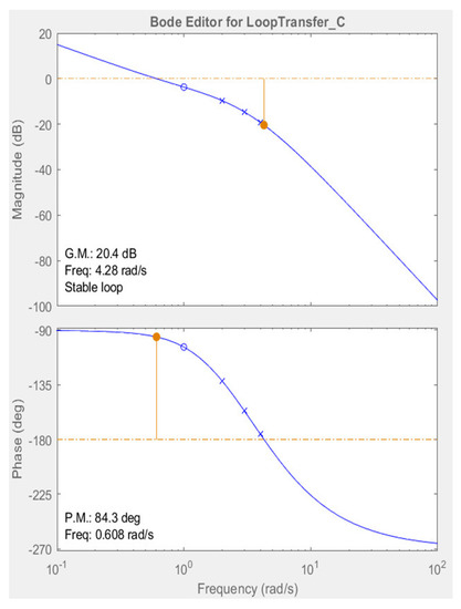
Figure A1.
Bode plot to observe stability of the proposed converter system.
Figure A1.
Bode plot to observe stability of the proposed converter system.
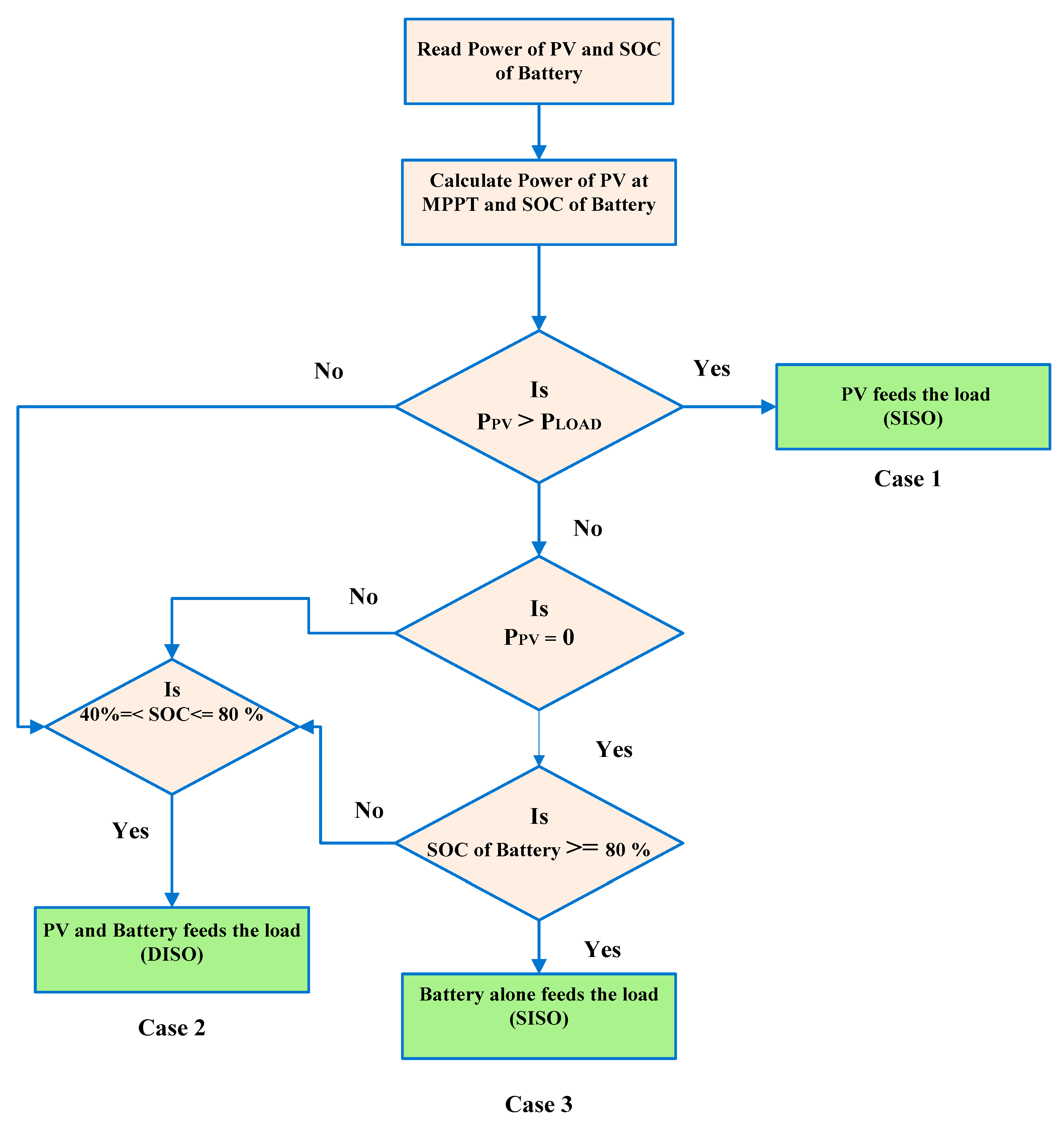
Appendix A.4. Control Algorithm Fed in the Controller
The control algorithm for the proposed converter is shown in Figure A2. The converter fed the load according to the PV and Battery conditions.

Figure A2.
Control algorithm for the proposed multiport converter.
Figure A2.
Control algorithm for the proposed multiport converter.
The results of MPPT algorithm representing the output of PV panel at variable irradiance are shown in Table A1. This algorithm was set in the MPPT controller. By applying the MPPT algorithm (fractional open circuit voltage technique), output power was obtained at maximum voltage. From the table, it was observed that the current varied with the irradiance and the maximum power was obtained at the highest irradiance.
Table A1.
Results of MPPT algorithm—output of PV panel at variable irradiance.
Table A1.
Results of MPPT algorithm—output of PV panel at variable irradiance.
| SL. NO | Irradiance (W/sq.m) | VPV (V) | I PV (A) | PPV (W) |
|---|---|---|---|---|
| 1 | 1000 | 37.42 | 7.3 | 273.17 |
| 2 | 800 | 36.86 | 6.6 | 243.28 |
| 3 | 600 | 36.80 | 5.3 | 195.04 |
| 4 | 400 | 36.7 | 4.3 | 154.14 |
| 5 | 200 | 36.7 | 2.3 | 84.41 |
| 6 | 100 | 36.7 | 1.8 | 66.06 |
| 7 | 0 | 36.7 | 0 | 0 |
Appendix A.5. Example of Calculated Efficiencies at Different Operating Modes
The calculation of efficiency at various operating modes of the multiport converter has been shown in Table A2.
- (i)
- PV to load
At 1000 W/m2 irradiance, PV is supplying the load. At 10 Ω and 15 Ω load, both PV and battery are supplying the load to provide a calculated efficiency of 94.02% and 94.37% respectively. In this circumstance, the converter was operating in a dual input single output mode (DISO).
- (ii)
- Battery to load
In the absence of irradiance from PV, the battery alone supplied the load and produced a calculated efficiency of 91.22%. Here, the converter was operating in a single input single output (SISO) mode.
- (iii)
- PV to battery
At 1000 W/m2 irradiance, PV was charging the battery at 35 Ω and 40 Ω load and at the same time supplying the load to provide a calculated efficiency of 92.35% and 91.73% respectively. Here, the converter is operating in a single input single output (SISO) and bidirectional mode.
Table A2.
Calculation of efficiency at various modes.
Table A2.
Calculation of efficiency at various modes.
| SL. NO | Irradiance (W/m2) | PV Panel | Battery | Total Input Power (W) | Load (Ohm) | Converter Output | Calculated Efficiency (%) | ||||||
|---|---|---|---|---|---|---|---|---|---|---|---|---|---|
| Vpv(V) | Ipv(A) | P pv(W) | Vb (V) | Ib (A) | Pb (W) | Vo (V) | Io (A) | Po (W) | |||||
| 1 | 1000 | 37.42 | 7.30 | 273.17 | 40 | 6.20 | 248.00 | 521.17 | 10 | 70.00 | 7.00 | 490.00 | 94.02 |
| 2 | 1000 | 37.42 | 7.30 | 273.17 | 40 | 1.80 | 72.00 | 345.17 | 15 | 69.90 | 4.66 | 325.73 | 94.37 |
| 3 | 1000 | 37.42 | 7.30 | 273.17 | 40 | −3.05 | −122.00 | 151.17 | 35 | 69.90 | 2.00 | 139.60 | 92.35 |
| 4 | 1000 | 37.42 | 7.30 | 273.17 | 40 | −3.50 | −140.00 | 133.17 | 40 | 69.90 | 1.75 | 122.15 | 91.73 |
| 5 | 0 | 36.70 | 0.00 | 0.00 | 40 | 8.90 | 356.00 | 356.00 | 15 | 69.90 | 4.65 | 324.76 | 91.22 |
References
- Alghaythi, M.L.; O’Connell, R.M.; Islam, N.E.; Khan, M.M.; Guerrero, J.M. A High Step-Up Interleaved dc-dc converter with voltage multiplier and coupled inductors for Reenwable energy systems. IEEE Access 2020, 8, 123165–123174. [Google Scholar] [CrossRef]
- Chub, A.; Vinnikov, D.; Blaabjerg, F.; Peng, F.Z. A review of galvanically isolated impedance-source DC–DC converters. IEEE Trans. Power Electron. 2016, 31, 2808–2828. [Google Scholar] [CrossRef]
- Onar, O.C.; Khaligh, A. A novel integrated magnetic structure based DC/DC converter for hybrid battery/ultracapacitor energy storage systems. IEEE Trans. Smart Grid 2012, 3, 296–307. [Google Scholar] [CrossRef]
- Li, X.; Bhat, A.K.S. Analysis and Design of High-Frequency Isolated Dual-Bridge Series Resonant DC/DC Converter. IEEE Trans. Power Electron. 2010, 25, 850–862. [Google Scholar] [CrossRef]
- Chen, Y.-M.; Liu, Y.-C.; Wu, F.-Y. Multi-input DC/DC converter based on the multiwinding transformer for renewable energy applications. IEEE Trans. Ind. Appl. 2002, 38, 1096–1104. [Google Scholar] [CrossRef]
- Li, Y.; Ruan, X.; Yang, D.; Liu, F.; Tse, C.K. Synthesis of Multiple-Input DC/DC Converters. IEEE Trans. Power Electron. 2010, 25, 2372–2385. [Google Scholar] [CrossRef]
- Dusmez, S.; Li, X.; Akin, B. A new multiinput three-level DC/DC converter. IEEE Trans. Power Electron. 2016, 31, 1230–1240. [Google Scholar] [CrossRef]
- Karthikeyan, V.; Gupta, R. Distributed power flow control using cascaded multilevel isolated bidirectional DC–DC converter with multi-phase shift modulation. IET Power Electron. 2019, 12, 2996–3003. [Google Scholar] [CrossRef]
- Irfan, M.S.; Ahmed, A.; Park, J.-H. Power–decoupling of a Multi-power Isolated Converter for an Electrolytic-capacitorless Multi-Level Inverter. IEEE Trans. Power Electron. 2017, 33, 6656–6671. [Google Scholar] [CrossRef]
- Khaligh, A.; Cao, J.; Lee, Y.-J. A Multiple-Input DC-DC Converter Topology. IEEE Trans. Power Electron. 2009, 24, 862–868. [Google Scholar] [CrossRef]
- Kathapalli, K.R.; Ramteke, M.R.; Suryawanshi, H.m.; Reddi, N.K.; Ka-lahasti, R.B. Soft switched Ultra High Gain DC-DC converter with Voltage Multiplier Cell for DC Microgrid. IEEE Trans. Ind. Electron. 2020, 99–110. [Google Scholar] [CrossRef]
- Qian, Z.; Abdel-Rahman, O.; Al-Atrash, H.; Batarseh, I. Modeling and Control of Three-Power DC/DC Converter Interface for Satellite Applications. IEEE Trans. Power Electron. 2010, 25, 637–649. [Google Scholar] [CrossRef]
- Qian, Z.; Abdel-Rahman, O.; Batarseh, I. An Integrated Four-Port DC/DC Converter for Renewable Energy Applications. IEEE Trans. Power Electron. 2010, 25, 1877–1887. [Google Scholar] [CrossRef]
- Khodabandeh, M.; Afshari; Amirabadi, M. A Family of Cuk-, Zeta-, and SEPIC-based Soft-Switching DC-DC Converters. IEEE Trans. Power Electron. 2019, 34, 9503–9519. [Google Scholar] [CrossRef]
- Tao, H.; Kotsopoulos, A.; Duarte, J.L.; Hendrix, M.A. Family of multiport bidirectional DC–DC converters. IEE Proc. Electr. Power Appl. 2006, 153, 54–65. [Google Scholar] [CrossRef] [Green Version]
- Banaei, M.R.; Sani, S.G. Analysis and Implementation of a New SEPIC-Based Single-Switch Buck–Boost DC–DC Converter with Continuous Input Current. IEEE Trans. Power Electron. 2018, 33, 10317–10325. [Google Scholar] [CrossRef]
- Andrade, A.M.; da Silva Martins, M.L. Quadratic-boost with stacked zeta converter for high voltage gain applications. IEEE J. Emerg. Sel. Top. Power Electron. 2017, 5, 1787–1796. [Google Scholar] [CrossRef]
- Falcones, S.; Ayyanar, R.; Mao, X. A DC-DC Multiport-Converter-Based Solid-State Tranaformer Integrating Distributed Generation and Storage. IEEE Trans. Power Electron. 2013, 28, 2192–2203. [Google Scholar] [CrossRef]
- Shrivastava, A.; Singh, B.; Pal, S. A Novel Wall-Switched Step-Dimming Concept in LED Lighting Systems using PFC Zeta Converter. IEEE Trans. Ind. Electron. 2015, 62, 6272–6283. [Google Scholar] [CrossRef]
- Narula, S.; Singh, B.; Bhuvaneswari, G. Power Factor Corrected Welding Power Supply Using Modified Zeta Converter. IEEE J. Emerg. Sel. Top. Power Electron. 2016, 4, 617–625. [Google Scholar] [CrossRef]
- Kumar, R.; Singh, B. BLDC Motor Driven Solar PV Array Fed Water Pumping System Employing Zeta Converter. IEEE Trans. Indusrty Appl. 2016, 52, 2315–2322. [Google Scholar] [CrossRef]
- Mishra, S.K.; Nayak, K.K.; Rana, M.S.; Dharmarajan, V. Switched-boost action based multiport converter. IEEE Trans. Ind. Appl. 2019, 55, 2315–2322. [Google Scholar] [CrossRef]
- Andrade, A.M.S.S.; Hey, H.L.; Schuch, L.; da Silva Martins, M.L. Comparative Evaluation of Singh Switch High-Voltage Step-Up Topologies Based on Boost and Zeta PWM Cells. IEEE Trans. Ind. Electron. 2018, 66, 2322–2334. [Google Scholar] [CrossRef]
- Wang, F.; Lei, Z.; Xu, X.; Shu, X. Topology Deduction and Analysis of Voltage Balancers for DC Micro-Grid. IEEE J. Emerg. Sel. Top. Power Electron. 2017, 5, 672–680. [Google Scholar] [CrossRef]
- Mishra, A.K.; Singh, B. Design of Solar-Powered Agriculture Pump using New Configuration of Dual-Output Buck-Boost Converter. IET Renew. Power Gener. 2018, 12, 1640–1650. [Google Scholar] [CrossRef]
- Zhu, B.; Liu, G.; Zhang, Y.; Huang, Y.; Hu, S. Sinlge switch high-step up Zeta converter based in Coat Circuit. IEEE Access 2021, 9, 5166–5176. [Google Scholar]
- Zeng, J.; Qiao, W.; Qu, L.; Jiao, Y. An Isolated Multiport DC-DC Converter for Simultaneous Power Management of Multiple Different Renewable Energy Sources. IEEE J. Emerg. Sel. Top. Power Electron. 2014, 2, 70–78. [Google Scholar] [CrossRef]
- Hwu, K.I.; Yau, Y.T. KY Converter and Its Derivatives. IEEE Trans. Power Electron. 2009, 24, 128–137. [Google Scholar] [CrossRef]
- Sedaghati, F.; Azizkandi, M.E.; Majareh, S.H.L.; Shayeghi, H. A High-Efficiency Non-Isolated High-Gain Interleaved DC-DC Converter with Reduced Voltage Stress on Devices. In Proceedings of the 10th International Power Electronics, Drive Systems and Technologies Conference (PEDSTC), Shiraz, Iran, 12–14 February 2019; pp. 729–734. [Google Scholar]
- Hwu, K.I.; Yau, Y.T. A KY Boost Converter. IEEE Trans. Power Electron. 2010, 25, 2699–2703. [Google Scholar] [CrossRef]
- Hwu, K.; Jiang, W. Improvement on voltage gain for KY converter. IET Power Electron. 2015, 8, 361–370. [Google Scholar] [CrossRef]
- Hwu, K.I.; Peng, T.J. A Novel Buck-Boost Converter Combining KY and Buck Converters. IEEE Trans. Power Electron. 2012, 27, 2236–2241. [Google Scholar] [CrossRef]
- Hwu, K.I.; Jiang, W.Z. Voltage Gain Enhancement for a Step-Up Converter Constructed by KY and Buck-Boost Converters. IEEE Trans. Ind. Electron. 2014, 61, 1758–1768. [Google Scholar] [CrossRef]
- Zhang, Y.; Li, D.; Lu, H.; Fan, S.; Chen, Z.; Wang, Y.; Geng, L. Analysis and Implementation of a High-Performance-Integrated KY Converter. IEEE Trans. Power Electron. 2017, 32, 9051–9064. [Google Scholar] [CrossRef]
- Kushwaha, R.; Singh, B. UPF-Isolated Zeta Converter-based Battery Charger for Electric Vehicle. IET Electr. Syst. Transp. 2019, 9, 103–112. [Google Scholar] [CrossRef]
- Durán, E.; Litrán, S.P.; Ferrera, M.B. Configurations of DC–DC converters of one input and multiple outputs without transformer. IET Power Electron. 2020, 13, 2658–2670. [Google Scholar] [CrossRef]
- Bhaskar, M.S.; Ramachandaramurthy, V.K.; Padmanaban, S.; Blaabjerg, F.; Ionel, D.M.; Mitolo, M.; Almakhles, D. Survey of DC-DC Non-Isolated Topologies for Unidirectional Power Flow in Fuel Cell Vehicles. IEEE Access 2020, 8, 178130–178166. [Google Scholar] [CrossRef]
- McDonough, M. Integration of inductively coupled Power Transfer and hybrid energy system: A Multi-Port Power Electronics interface for Battery Powered Electric Vehicles. IEEE Trans. Power Electron. 2015, 30, 6423–6433. [Google Scholar] [CrossRef]


Publisher’s Note: MDPI stays neutral with regard to jurisdictional claims in published maps and institutional affiliations. |
© 2021 by the authors. Licensee MDPI, Basel, Switzerland. This article is an open access article distributed under the terms and conditions of the Creative Commons Attribution (CC BY) license (https://creativecommons.org/licenses/by/4.0/).