Abstract
Quantum-dot cellular automata (QCA) nanotechnology is a practical suggestion for replacing present silicon-based technologies. It provides many benefits, such as low power usage, high velocity, and an extreme density of logic functions on a chip. In contrast, designing circuits with no waste of information (reversible circuits) may further reduce energy losses. The Feynman gate has been recognized as one of the most famous QCA-based gates for this purpose. Since reversible gates are significant, this paper develops a new optimized reversible double Feynman gate that uses efficient arithmetic elements as its key structural blocks. Additionally, we used several modeling principles to make it consistent and more robust against noise. Moreover, we examined the suggested model and compared it to the previous models regarding the complexity, clocking, number of cells, and latency. Furthermore, we applied QCADesigner to monitor the outline and performance of the proposed gate. The results show an acceptable improvement via the designed double Feynman gate in comparison to the existing designs. Finally, the temperature and cost analysis indicated the efficiency of the proposed nan-scale gate.
1. Introduction
Over the last 20 years, scholars have always used silicon-based procedures to meet the necessary dimension scaling for executing high-velocity, high-density, and low-energy VLSI devices []. Nevertheless, an aggressive scaling such as that certainly has numerous challenges, including high power density, high leakage current, and expensive lithography. Scholars have forecasted that the above challenges will lead to the end of the CMOS revolution in the coming years [,,]. The abovementioned background brings about the necessity of researching new nano-scale technologies to introduce reliable alternatives []. Quantum-dot cellular automata (QCA) addresses the related nano-scale issues and provides a novel technique for processing and transforming the information [,,]. It has ultra-low feature size and power usage []. The researchers asserted that it is possible to make nano-scale QCA cells by means of molecular execution, using a self-assembly procedure [,,,].
Nanotechnology has become the core of many recent high-level technologies, and the QCA can be a revolutionary method for nano-processing []. Parallel and reversible logic is becoming a noticeable technology that improves QCA technology performance []. Scholars have reported several works on reversible logic gates and their execution [,,,,,]. Numerous reversible logic gates exist [,]; they are essential for their reversibility features, and the Feynman gate is a crucial one. This paper proposes a new double Feynman gate circuit using the reversible gate []. We have applied a set of reversible logic gates in which each input has a one-to-one relationship with each output []. Additionally, the number of the input and output gates is equal. Since reversible circuits can identify and modify the output faults, identifying and modifying faults would be easier than simple designs [,]. There is no info loss in a reversible circuit []. Then, it provides the highest output information and makes error identification possible. We applied the Feynman gate to generate a new reversible gate in QCA technology in the current study. Briefly, the present article contributes to the following:
- Introducing a coplanar structure for a reversible double Feynman gate with a lower usage space and cell count;
- Comparing the proposed model to existing ones regarding cell counts, delay, layer, cost, and average output polarization.
2. Related Work
Scholars have presented various designs for the reversible gate and circuit []. Here, we summarize and compare the major reversible models and circuits in QCA technology. The reversible gates can be considered as construction parts of the reversible logic. The researchers offered exclusive mapping among the vectors of output and input. Thus, the input count should be similar to the output amount. Figure 1 indicates some block diagrams of the major reversible gates proposed in the past.
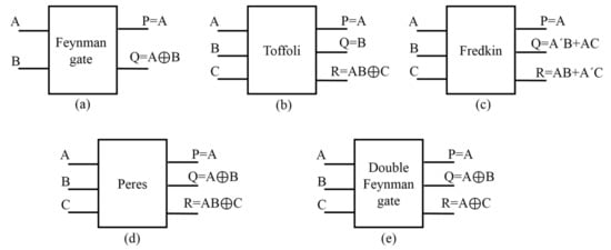
Figure 1.
The block diagrams of the reversible gates: (a) the Feynman [], (b) the Toffoli [], (c) the Fredkin [], (d) the Peres [], and (e) the double Feynman gate [].
Figure 1a indicates the Feynman gate’s block diagram, and Figure 2 indicates its implementation based on QCA. Figure 3a indicates the block diagram of the double Feynman gate, and Figure 3b indicates its QCA. The output vector is O (R, P, and Q), and the input vector is I (B, C, A). R = A ⨁ C, Q = A ⨁ B, P = A specify the output. The truth table of the gate is illustrated in Table 1.
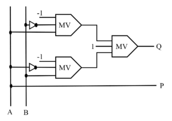
Figure 2.
The diagram of the Feynman gate in the QCA [].
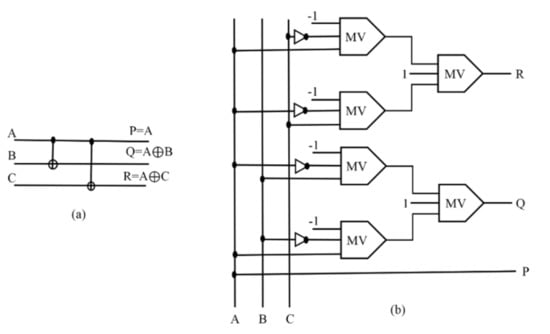
Figure 3.
(a) The logical diagram of the double Feynman gate, and (b) the QCA-based diagram of the double Feynman gate [].

Table 1.
The truth table of the double Feynman gate.
Researchers have proposed numerous reversible gates. The NOT and BUFFER are the simplest ones (“1 × 1”). The Feynman gate is the famous “2 × 2” reversible gate []. It can be applied to have more fan-out. Figure 1a indicates the symbol of the Feynman gate. The Toffoli [] (Figure 1b), Peres [] (Figure 1d), and Fredkin [] (Figure 1c) gates are the famous “3 × 3” reversible gates. The Toffoli gate works similarly to the Feynman gate; its single variance is that it has two control input lines. The universal gate means that we can synthesize all digital gates using it. The self-compliment gate means that if we use two Toffoli gates serially, the output of the second one would be identical to the input of the first one. Figure 1e indicates the double Feynman gate, plotting inputs (A, B, C) to outputs (Q = A ⊕ B, R = A ⊕ C, P = A) [].
Bahar, Waheed [] proposed two new methods for modeling a double Feynman gate (F2G) by QCA. They simulated them by QCADesigner and examined them regarding the intricacy (cell count) and space. The outcomes indicated that the introduced circuits have proper functionality. The first circuit has 51 cells arranged in a 0.06 space; they obtained its results after three cycles delay. The second circuit has 96 cells arranged in a 0.93 space. Figure 4a shows the layout of their first double Feynman gate, and Figure 4b shows their second double Feynman gate. The designs are promising for the upcoming processing methods, such as ultra-low-power quantum computers and digital circuits. They use three three-input majority and four inverter gates.
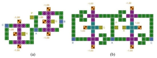
Figure 4.
The layout of the double Feynman gates (proposed by Bahar, Waheed []): (a) the first design for double Feynman gates, and (b) the second design for double Feynman gates.
Furthermore, Sasamal, Singh [] proposed an area-efficient and power-efficient reversible logic gate by the QCA. Using a two-input XOR gate, their models reached better functionality than NOT and BUFFER. They compared their functionality with those of the existing ones using the conventional metrics. Figure 5 shows the layout of their proposed gate. The number of QCA cells is less than other designs. Their proposed gate also reached 0.5 clock cycles delay. The power analysis verified that the introduced gate has a low energy dissipation. Thus, the introduced structure can improve the intricate nano-scale circuits’ total functionality in the QCA. Figure 5 shows the double Feynman gate, plotting inputs (A, B, C) to outputs (Q = A ⊕ B, R = A ⊕ C, P = A). In this architecture, an extra gate is needed (for output P), while the two two-input XOR gates need the outputs R and Q. The introduced outline incorporates the XOR architecture with no necessity for three-input majority gates, in contrast with the existing models.
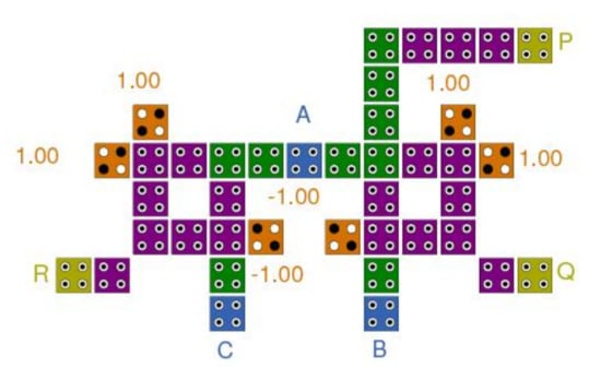
Figure 5.
The layout of the double Feynman gate (proposed by Sasamal, Singh []).
Finally, Parhami [] proposed a “Feynman double-gate”. Figure 6 shows his proposed “Feynman double-gate”. Considering the additional input and output and the control input A, he determined another controlled-NOT operation. His Feynman double-gate has its own inverse, as with the Feynman and the Fredkin. He introduced a QCA architecture for diverse reversible gates with a three-input majority gate as the primary unit. Still, a few outputs are not greatly polarized. For example, the output P is 8.63 × 10⁻³ and 5.80 × 10⁻³ for the Fredkin and Peres gates, respectively. Based on the results, the output misses the input signal above 14%, influencing model drivability.
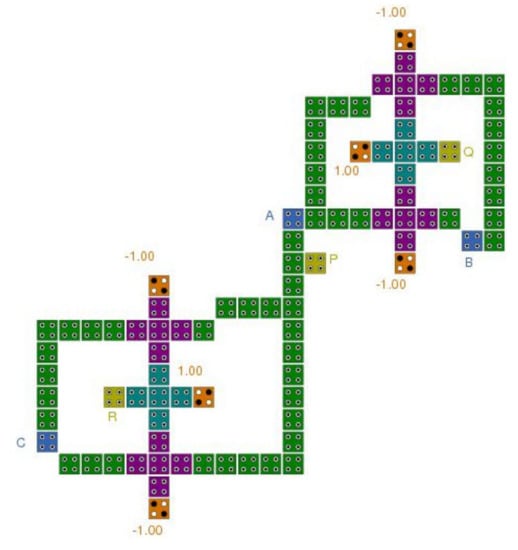
Figure 6.
The layout of the Feynman double-gate (proposed by Parhami []).
3. Proposed Design
We propose a new reversible double Feynman gate in QCA technology implemented by the majority gates and XOR ones in the present study []. Our method converts multi-output irreversible functions into reversible ones. Hence, a reversible function has some characteristics listed below:
- A unique mapping exists among the inputs and outputs.
- Feedback is not acceptable.
- Fan-out is not permitted.
However, according to [,], characteristics 2 and 3 are not essential for generating reversible functions in the QCA. Thus, we should create a one-to-one mapping among the inputs and outputs to convert the multi-output functions into reversible ones. We know numerous crucial reversible logic gates in the QCA technology. An n-input n-output logic device is a reversible logic gate with a unique mapping that specifies the outputs from the inputs and solely recovers the inputs. The Feynman gate has been considered to be a 2 × 2 gate; it is also known as controlled-NOT. O (P, Q) is known to be the output vector, while I (A, B) is considered the input vector. P = A, Q = A ⨁ B [Q = MV (MV (A’, B, −1), MV (A, B’, −1), 1] specifies the output.
A new optimized QCA-based double Feynman gate is presented utilizing three-input majority gates, along with the inverter gates. Figure 3 demonstrates mapping the inputs (A, B, C) to the outputs (R = A ⊕ C, Q = A ⊕ B, P = A) and the diagram of the introduced double Feynman gate. As shown in Figure 3, the primary logical figure for executing the double Feynman gate in the QCA has two key elements; six three-input majority gates and four inverter gates. This double Feynman gate was implemented in QCA technology with 46 cells and in an space, and simulated in the coplanar layer. Figure 7 indicates the QCA outline of the introduced double Feynman gate that operates in three clock zones, creates the two outputs R and Q in two clock zones, and establishes P output in one clock zone. In this double Feynman gate, the R and Q signals are supplied by three majority gates and two inverter ones.
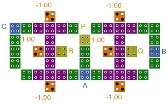
Figure 7.
The proposed design of the double Feynman gate based on majority gates.
4. Results
In this part, the suggested QCA layout is evaluated and compared to current designs.
4.1. Simulation Tools
In the present study, the QCADesigner was used to build a quick and precise simulation and layout device for the QCA []. A key feature of the design is that the developers can easily simulate their designs in the QCADesigner. In addition, a standardized calling system and data formats make it simple to connect simulation engines into the QCADesigner. The existing version has two simulation engines [,,,]. In the QCADesigner, every single cell can be in one of four states (input, output, fixed, or normal). Figure 8 shows these modes.
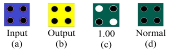
Figure 8.
Cells in QCADesigner: (a) input cell, (b) output cell, (c) fixed and (d) normal [].
4.2. Simulation Parameters
In the QCADesigner tool, the whole simulation computations and parameters have been adjusted to their default levels. Each cell’s size is regulated to 18 × 18 nm2 with 5 nm diameter quantum dots. Bistable approximation factors have been set to 12.9 relative permittivity, 0.001 convergence tolerance, 9.8 × 10⁻²² J clock high, 3.8 × 10⁻²³ J clock low, 11.5 nm layer separation, and 100 iterations per sample. The defined parameters in Table 2 were used for “Coherence Vector” and “Bistable Approximation” engines [,]. In this study, the simulation engine was set to “Bistable Approximation” and “Coherence Vector,” and we used both of them to simulate the proposed circuit.
Table 2.
QCADesigner parameters for “Coherence Vector” and “Bistable Approximation”.
4.3. Accuracy Analysis
This section demonstrates the results for the introduced circuits and compared them to those of the other circuits. Figure 9 shows the simulation results based on all combinations of A, B, and C inputs. The simulation outcomes confirmed that the suggested gate conducts well and designates the relevant production. In our model, A, B, and C are identified as inputs and P, Q, and R as the output cells. For example, Figure 9 demonstrates the right outputs of the proposed gate for inputs A = 1, B = 1, and C = 0, which are P = 1, Q = 0, and R = 1. The first significant waveform from P was produced at clock one. This design is coplanar. The desired outputs were collected from the coplanar layer. Based on Figure 9, we can understand the forceful polarization of the majority gates’ output cell.
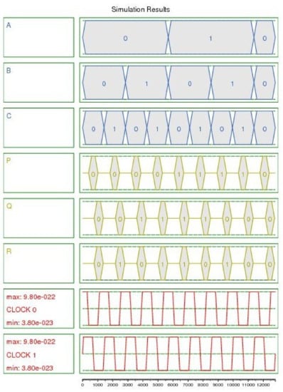
Figure 9.
Simulation outcomes of the proposed double Feynman gate.
4.4. Comparisons
The simulation outcomes showed the correct operation of the proposed gate. Additionally, Table 3 demonstrates the comparison between the suggested double Feynman gate and the best existing gates. The comparison shows that the proposed method outperformed or is similar to the other ones regarding reducing the required space and cell counts. It has a compact architecture and lower cell counts than the best previous designs. When compared to the best-presented QCA double Feynman gate design with the majority gate, our designs result in a 10% increase in cell counts. Additionally, as indicated in Equations (1) and (2), significant design measurements such as the area latency product (ALP) and cost function can assess the efficiency of the QCA designs []:
Table 3.
Comparison among the proposed and previous models.
Table 3 compares the proposed design in terms of ALP and cost to the other state-of-the-art designs.
Furthermore, we can use another cost function named the QCA cost function to measure the proposed double Feynman gate’s complexity. The QCA cost function (for majority gate-based circuits) is expressed as follows []:
where I is the number of inverters, M is the number of majority gates, T is the circuit’s delay, and C is the number of crossovers. Additionally, k, l, p are the weights for majority gate, crossover, and delay, respectively. In this part, different values (between 1 and 4) are considered for these weights to compare them better. As shown in Table 4, the suggested double Feynman gate is among the best circuits offered in terms of cost. The proposed design cost in four different types of experiment is better than the proposed designs in [,].
Table 4.
QCA cost for the proposed reversible double Feynman gate and other layouts.
The temperature influence on the output cell polarization of the reversible gate is also very important. To test the average output polarization (AOP), QCADesigner can also be applied with a coherent vector stimulation device []. The AOP function is expressed as follows []:
Table 5 demonstrates the AOPs for each output cell of the suggested gate and novel schemes. In a range of 1–7 K (a typical temperature range in this technology), the suggested circuit performs efficiently, and the AOP is changed very slightly. These outcomes illustrate that the suggested model outperforms previous designs regarding stability in a diverse temperature range. As a result, the suggested design is extremely stable when the temperature is changed.
Table 5.
AOP for the proposed reversible double Feynman gate.
5. Conclusions and Future Work
High velocity, low power utilization, and high density make the QCA an appropriate nano-scale substitute for the CMOS. In contrast, the reversible double Feynman gate is a crucial circuit in logical processes. We proposed a new QCA architecture for a reversible double Feynman gate and simulated it by means of the QCAdesigner. The outcomes indicated that the introduced circuit in the present study generated a precise output. Thus, it has suitable functionality and performed better regarding cell counts, space, and time delay than previous designs. The simulation outcomes indicated that the model meaningfully reduced the required latency and cell number. The proposed coplanar double Feynman gate outperformed the other models (single-layer with coplanar application of a majority gate) regarding the number of cells and latency.
Based on the obtained results, we confirmed the efficiency of the proposed design. It can be useful for designing more intricate and better reversible QCA circuits. We can also use it as a useful construction block for bigger units to plan a reversible circuit. Finally, an n-bit Feynman gate can be designed by linking the proposed double Feynman gates in order to use less hardware.
Author Contributions
Conceptualization, S.S. and A.O.; methodology, S.S. and N.J.N.; software, S.S.; validation, S.S., A.O. and N.J.N.; investigation, A.O. and N.J.N.; resources, S.S.; writing—original draft preparation, S.S. and N.J.N.; writing—review and editing, A.O.; supervision, N.J.N.; project administration, N.J.N. All authors have read and agreed to the published version of the manuscript.
Funding
This research received no external funding.
Conflicts of Interest
The authors declare no conflict of interest.
References
- Bahar, A.N.; Waheed, S.; Uddin, M.A.; Habib, M.A. Double Feynman gate (F2G) in quantum-dot cellular automata (QCA). Int. J. Comput. Sci. Eng. 2013, 2, 351–355. [Google Scholar]
- Parvin, S.; Altun, M. Perfect Concurrent Fault Detection in CMOS Logic Circuits Using Parity Preservative Reversible Gates. IEEE Access 2019, 7, 163939–163947. [Google Scholar] [CrossRef]
- Siccardi, S.; Adamatzky, A. Actin quantum automata: Communication and computation in molecular networks. Nano Commun. Netw. 2015, 6, 15–27. [Google Scholar] [CrossRef]
- Das, J.C.; De, D. Nanocommunication network design using QCA reversible crossbar switch. Nano Commun. Netw. 2017, 13, 20–33. [Google Scholar] [CrossRef]
- Martins Bezerra, P.A.; Krismer, F.; Kolar, J.W.; Khaddam-Aljameh, R.; Paredes, S.; Heller, R.; Brunschwiler, T.; Francese, P.; Morf, T.; Kossel, M.; et al. Experimental Efficiency Evaluation of Stacked Transistor Half-Bridge Topologies in 14 nm CMOS Technology. Electronics 2021, 10, 1150. [Google Scholar] [CrossRef]
- Weder, B.; Barzen, J.; Leymann, F.; Salm, M. Automated Quantum Hardware Selection for Quantum Workflows. Electronics 2021, 10, 984. [Google Scholar] [CrossRef]
- Orlov, A.; Amlani, I.; Bernstein, G.H.; Lent, C.; Snider, G.L. Realization of a Functional Cell for Quantum-Dot Cellular Automata. Science 1997, 277, 928–930. [Google Scholar] [CrossRef] [Green Version]
- Hayati, M.; Rezaei, A. Design of a New Optimized Universal Logic Gate for Quantum-Dot Cellular Automata. IETE J. Res. 2019, 1–7. [Google Scholar] [CrossRef]
- Fam, S.R.; Navimipour, N.J. Design of a loop-based random access memory based on the nanoscale quantum dot cellular automata. Photon-Netw. Commun. 2018, 37, 120–130. [Google Scholar] [CrossRef]
- Ahmadpour, S.-S.; Mosleh, M.; Heikalabad, S.R. Efficient designs of quantum-dot cellular automata multiplexer and RAM with physical proof along with power analysis. J. Supercomput. 2021, 1–24. [Google Scholar] [CrossRef]
- Hennessy, K.; Lent, C.S. Clocking of molecular quantum-dot cellular automata. J. Vac. Sci. Technol. B Microelectron. Nanometer Struct. 2001, 19, 1752. [Google Scholar] [CrossRef] [Green Version]
- Gupta, P.; Jha, N.K.; Lingappan, L. A Test Generation Framework for Quantum Cellular Automata Circuits. IEEE Trans. Very Large Scale Integr. (VLSI) Syst. 2007, 15, 24–36. [Google Scholar] [CrossRef]
- Seyedi, S.; Navimipour, N.J. Design and evaluation of a new structure for fault-tolerance full-adder based on quantum-dot cellular automata. Nano Commun. Netw. 2018, 16, 1–9. [Google Scholar] [CrossRef]
- Debnath, B.; Das, J.C.; De, D.; Mondal, S.P.; Ahmadian, A.; Salimi, M.; Ferrara, M. Security Analysis with Novel Image Masking Based Quantum-Dot Cellular Automata Information Security Model. IEEE Access 2020, 8, 117159–117172. [Google Scholar] [CrossRef]
- Khosroshahy, M.B.; Moaiyeri, M.H.; Navi, K.; Bagherzadeh, N. An energy and cost efficient majority-based RAM cell in quantum-dot cellular automata. Results Phys. 2017, 7, 3543–3551. [Google Scholar] [CrossRef]
- Safoev, N.; Jeon, J.-C. Design and Evaluation of Cell Interaction Based Vedic Multiplier Using Quantum-Dot Cellular Automata. Electronics 2020, 9, 1036. [Google Scholar] [CrossRef]
- Bahar, A.N.; Waheed, S.; Habib, A.; Habib, M.A. A novel presentation of reversible logic gate in Quantum-dot Cellular Automata (QCA). In Proceedings of the 2014 International Conference on Electrical Engineering and Information & Communication Technology, Dhaka, Bangladesh, 10–12 April 2014; pp. 1–6. [Google Scholar]
- Das, J.C.; De, D. Reversible Binary to Grey and Grey to Binary Code Converter using QCA. IETE J. Res. 2015, 61, 223–229. [Google Scholar] [CrossRef]
- Abdullah-Al-Shafi, M.; Shifatul, M.; Newaz, A. A Review on Reversible Logic Gates and its QCA Implementation. Int. J. Comput. Appl. 2015, 128, 27–34. [Google Scholar] [CrossRef]
- Rahman, M.A.; Khatun, F.; Sarkar, A.; Huq, M.F. Design and implementation of Feynman gate in quantum-dot cellular automata (QCA). Int. J. Comput. Sci. Issues 2013, 10, 167. [Google Scholar]
- Seyedi, S.; Navimipour, N.J. An Optimized Three-Level Design of Decoder Based on Nanoscale Quantum-Dot Cellular Automata. Int. J. Theor. Phys. 2018, 57, 2022–2033. [Google Scholar] [CrossRef]
- Debnath, B.; Das, J.C.; De, D.; Ghaemi, F.; Ahmadian, A.; Senu, N. Reversible Palm Vein Authenticator Design with Quantum Dot Cellular Automata for Information Security in Nanocommunication Network. IEEE Access 2020, 8, 174821–174832. [Google Scholar] [CrossRef]
- Noorallahzadeh, M.; Mosleh, M.; Ahmadpour, S.-S. Efficient Designs of Reversible Synchronous Counters in Nanoscale. Circuits Syst. Signal Process. 2021, 1–14. [Google Scholar] [CrossRef]
- Das, J.C.; De, D.; Mondal, S.P.; Ahmadian, A.; Ghaemi, F.; Senu, N. QCA Based Error Detection Circuit for Nano Communication Network. IEEE Access 2019, 7, 67355–67366. [Google Scholar] [CrossRef]
- Seyedi, S.; Navimipour, N.J. An optimized design of full adder based on nanoscale quantum-dot cellular automata. Optik 2018, 158, 243–256. [Google Scholar] [CrossRef]
- Feynman, R.P. Quantum mechanical computers. Found. Phys. 1986, 16, 507–531. [Google Scholar] [CrossRef]
- Toffoli, T. Reversible computing. In International Colloquium on Automata, Languages, and Programming; Springer: Berlin/Heidelberg, Germany, 1980; pp. 632–644. [Google Scholar]
- Fredkin, E.; Toffoli, T. Conservative Logic. In Collision-Based Computing; Springer: Berlin/Heidelberg, Germany, 2002; pp. 47–81. [Google Scholar]
- Peres, A. Reversible logic and quantum computers. Phys. Rev. A 1985, 32, 3266–3276. [Google Scholar] [CrossRef]
- Parhami, B. Fault-Tolerant Reversible Circuits. In Proceedings of the 2006 Fortieth Asilomar Conference on Signals, Systems and Computers, Pacific Grove, CA, USA, 29 October–1 November 2006; pp. 1726–1729. [Google Scholar]
- Sasamal, T.N.; Singh, A.K.; Ghanekar, U. Toward Efficient Design of Reversible Logic Gates in Quantum-Dot Cellular Automata with Power Dissipation Analysis. Int. J. Theor. Phys. 2017, 57, 1167–1185. [Google Scholar] [CrossRef]
- Balali, M.; Rezai, A.; Balali, H.; Rabiei, F.; Emadi, S. Towards coplanar quantum-dot cellular automata adders based on efficient three-input XOR gate. Results Phys. 2017, 7, 1389–1395. [Google Scholar] [CrossRef]
- Timler, J.; Lent, C.S. Maxwell’s demon and quantum-dot cellular automata. J. Appl. Phys. 2003, 94, 1050–1060. [Google Scholar] [CrossRef] [Green Version]
- Lent, C.S.; Liu, M.; Lu, Y. Bennett clocking of quantum-dot cellular automata and the limits to binary logic scaling. Nanotechnology 2006, 17, 4240–4251. [Google Scholar] [CrossRef] [Green Version]
- Walus, K.; Dysart, T.J.; Jullien, G.A.; Budiman, R.A. QCADesigner: A Rapid Design and Simulation Tool for Quantum-Dot Cellular Automata. IEEE Trans. Nanotechnol. 2004, 3, 26–31. [Google Scholar] [CrossRef]
- Chabi, A.M.; Sayedsalehi, S.; Angizi, S.; Navi, K. Efficient QCA Exclusive-or and Multiplexer Circuits Based on a Nanoelectronic-Compatible Designing Approach. Int. Sch. Res. Not. 2014, 2014, 1–9. [Google Scholar] [CrossRef] [PubMed]
- Kim, K.; Wu, K.; Karri, R. Quantum-dot cellular automata design guideline. IEICE Trans. Fundam. Electron. Commun. Comput. Sci. 2006, 89, 1607–1614. [Google Scholar] [CrossRef] [Green Version]
- Walus, K. ATIPS Laboratory QCADesigner Homepage. ATIPS Laboratory, Univ. Calgary, Calgary, AB, Canada. IEEE Trans. Nanotechnol. 2004, 3, 26–31. [Google Scholar] [CrossRef]
- Berggren, K.F.; Yakymenko, I. Quantum Cellular Automata-Theory, Experimentation and Prospects; Imperial College Press: London, UK, 2006. [Google Scholar]
- Singh, R.; Sharma, D.K. Design of efficient multilayer RAM cell in QCA framework. Circuit World 2020, 47, 31–41. [Google Scholar] [CrossRef]
- Liu, W.; Lu, L.; O’Neill, M.; Swartzlander, E.E. A First Step Toward Cost Functions for Quantum-Dot Cellular Automata Designs. IEEE Trans. Nanotechnol. 2014, 13, 476–487. [Google Scholar] [CrossRef]
- Pudi, V.; Sridharan, K. Efficient Design of a Hybrid Adder in Quantum-Dot Cellular Automata. IEEE Trans. Very Large Scale Integr. (VLSI) Syst. 2010, 19, 1535–1548. [Google Scholar] [CrossRef]
- Abdullah-Al-Shafi, M.; Bahar, A.N.; Bhuiyan, M.M.R.; Shamim, S.M.; Ahmed, K. Average output polarization dataset for signifying the temperature influence for QCA designed reversible logic circuits. Data Brief 2018, 19, 42–48. [Google Scholar] [CrossRef]
Publisher’s Note: MDPI stays neutral with regard to jurisdictional claims in published maps and institutional affiliations. |
© 2021 by the authors. Licensee MDPI, Basel, Switzerland. This article is an open access article distributed under the terms and conditions of the Creative Commons Attribution (CC BY) license (https://creativecommons.org/licenses/by/4.0/).