1. Introduction
The recent research trend in the emerging fields of high-density power electronics, such as avionics, space or marine applications, has imposed new design challenges to make the modern AC-DC rectifier systems, like active boost Power Factor Correction (PFC) converters, comply with the stringent requirements in terms of efficiency, reliability, volume, weight, line harmonics and, finally, EMI [
1,
2,
3,
4,
5]. Moreover, as the industry demands more power dense converters with lighter weight and volume, the switching frequency of the converter must be increased in order to lower the passive component volume. In order to restrict the frequency-related losses in the switching semiconductor devices, the employment of wide-bandgap semiconductor devices, such as Silicon-carbide (SiC) and Gallium Nitride (GaN) MOSFETs, become an obvious choice due to their faster switching transients and lower device parasitics. The presence of power stage non-idealities in any power converter, such as stray inductances, parasitic capacitances of switching devices and inter/intra winding capacitances of the inductor/transformer, give rise to voltage- and current-mode EMI noise sources that tend to propagate towards the AC grid and/or chassis (or potential earth), resulting in increased leakage current and grid pollution. Compared to Si devices, the WBG devices, such as Gallium Nitride (GaN) and Silicon Carbide (SiC), have higher dv/dt and di/dt switching transient rates. Therefore, the noise peak amplitudes in the EMI spectrum would be even higher for WBG-based power converters. The noise attenuation requirement that needs to be met by the EMI filter stage in a WBG-based power converter is likely to be higher than a Si-based design at the same switching frequency, which makes the filter bulkier and heavier in a WBG-based design [
6,
7]. This challenges the major motivation behind the use of the WBG devices, because while the converter stage can be made to be more power dense with WBG employment, the front-end EMI filter volume and weight tend to be higher, which may not give a significant net benefit of power density. Therefore, there needs to be significant research focus on EMI filter volumetric optimization for enabling WBG-based high-density power conversion, which is highly overlooked in the current research. Volume- and weight-optimized filter design solutions are critical for EMI stringent applications, with power density being the priority, such as power electronics for avionics and space, because a stricter noise attenuation requirement naturally makes the filter to be bulkier and heavier.
The conducted EMI noise in any power electronic circuit can appear in two forms: differential mode (DM) and common mode (CM). Two separate filters, commonly named as DM and CM Filters [
8,
9,
10,
11,
12,
13,
14,
15,
16,
17], are designed and employed in the front end of the power converter to sufficiently attenuate the conducted DM and CM EMI noises.
Although there are studies which have been carried out in order to optimally design the DM and CM EMI filter stages for any specific power converter application [
13,
14,
15,
16,
17,
18,
19], a systematic and mathematical design methodology that takes care of the following aspects is still absent: (a) selection of the optimum LC component values for minimum per-stage filter volume, (b) optimal number of filter stages considering the power factor constraint and attenuation requirement, (c) precise volumetric model of filter elements and (d) best choice of EMI filter structure with optimum arrangement of X and Y capacitors leading to the smallest volume. As the DM filter components form a major part of the converter size [
13,
18], EMI filter power density improvement is as critical as that of a converter power stage. Although a few techniques on volume optimization for the DM filter have been proposed in [
13,
16,
17,
18], the precision of the filter optimization process has been largely negotiated due to the compromise of precision in the quantitative cost function formulations, corresponding to the volume of the DM filter stages. In [
16], a volumetric comparison between two EMI filter structures for a three phase PFC is presented. However, both the filter structures were not optimized using a particular volume optimized filter design procedure. Thus, such a comparison may lead to an erroneous conclusion while choosing the best filter arrangement for any application. In this paper, firstly, a systematic and detailed design optimization methodology for volume minimization of the DM filter has been presented. Furthermore, we have proposed precise volumetric cost function models of the DM filter passive elements, in which the volumes of passive components are quantified as linear combinations of current/voltage, element value and their stored energy. Furthermore, applying this filter optimization technique on three different three-phase EMI filter structures, a volumetric comparison study was performed, which showed the dependency of the filter element arrangements on the maximum attainable power density.
The major contributions of the work are as follows:
(a) A systematic approach to design the EMI filter for any power converter, while addressing all possible design constraints, such as input power factor at light load and maximum allowable leakage current.
(b) Variance minimization-based statistical modeling that quantitatively corelates the DM filter components’ volume with rated current/voltage and filter element values.
(c) Multi-objective constrained volume optimization of the DM filter based on the proposed quantified models of the filter element volumes.
(d) A volumetric comparison study showing the dependency of the filter element arrangements on the maximum attainable power density.
This paper has been organized as follows.
Section 2 presents a brief overview of the three phase noise components present in any three-phase power converter. Comprehensive design criteria and constraints for the DM and CM stage EMI filter design are introduced and analyzed in
Section 3.
Section 4 explores the synthesis of possible three phase EMI Filter structures and their DM, CM equivalent circuits. The proposed volumetric optimization methodology is described in
Section 5. This section also examines the volumetric comparison between the various optimized filter structures under study. The filter design process and the mathematically deduced comparative volume data are validated through simulations and experimental results, presented in
Section 5.
Section 6 sums up the conclusions of this work with relevant discussions.
2. Three Phase Noise Components: A Brief Review
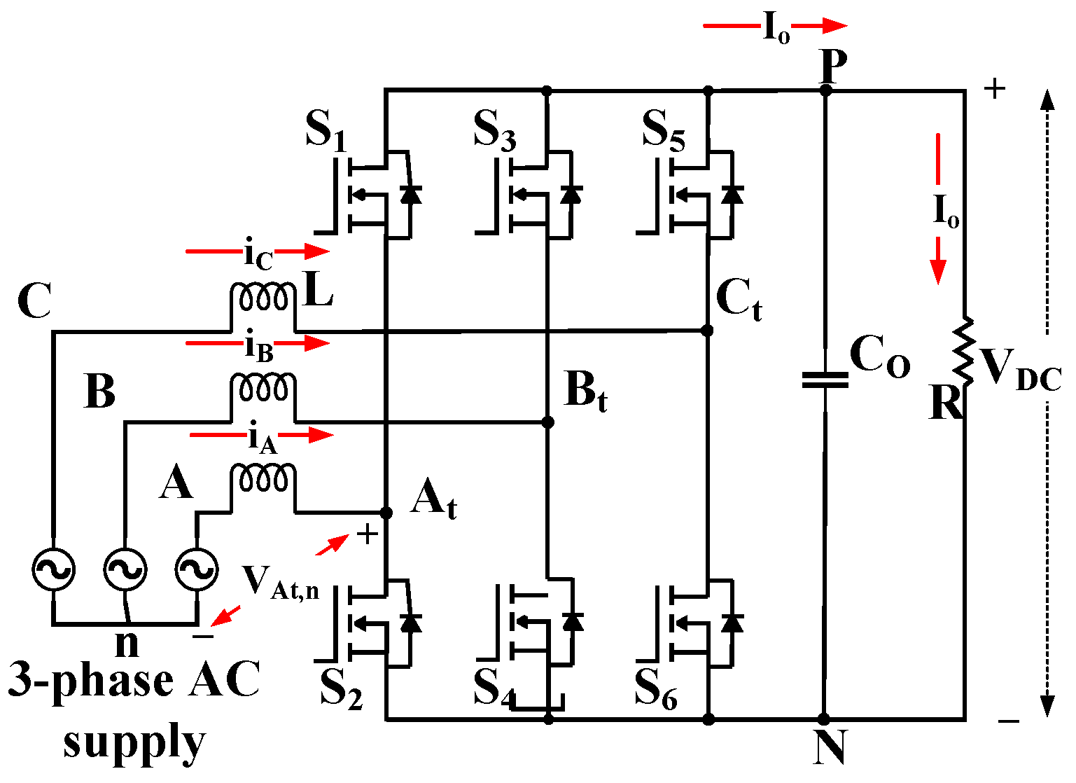
To design the EMI filter stage of a three-phase power converter to meet the standard requirements, an effective action would be to build a generalized model of the system noises appearing across the circuit. Some of the strong sources of EMI noise generation in any power converter are parasitics (such as drain-source-gate junction capacitances) corresponding to the semiconductor devices, attached heatsinks, inter/intra-winding capacitances and stray inductances. Here, a detailed review of the DM and CM noise components in a three-phase active boost rectifier, shown in
Figure 1, is provided.
Modeling of the noise components in a three-phase power converter system has been explored in [
1,
2]. A similar method to model the DM and CM noise components in our designed three phase PFC rectifier is taken up in this work. The CM current, for a three-phase power electronic converter, is defined as the total current that flows out through the phases and returns via protective earth. Therefore, it can be expressed as the sum of all three phase currents, as expressed in (1).
On the other side, the DM current runs through the one phase and comes back through the other two phases. This essentially indicates that the sum of the three phase DM current components is zero, as shown in (2).
The generalized high-frequency noise model of the three-phase power converter system is depicted in
Figure 2. Here, the three 50 Ω resistors, represented as
, model the line impedance stabilization network (LISN). The DM noise source corresponding to each phase is presented as
, with their respective source impedance
. Conversely, the CM noise source
is denoted as a lumped model with a single lumped impedance
to earth. The proposed noise model indicates separate current propagation paths for the CM and DM mode, which, however, may not hold true in real case scenarios. If current and voltage signals at the interconnections of the device under test to the LISN are considered, the definition of (1) is still valid, even if coupled noise propagation paths exist. The CM voltage at LISN, given in (3), is determined by the per-phase equivalent noise model.
The noise source in each phase is formed by a combination of corresponding CM and DM components; the equivalent DM voltage at the
phase is computed by employing KVL at the specific loop:
Therefore, the phase 1 DM voltage component is expressed as
. Assuming a symmetrical distribution of the CM current
in all the three phases, each phase current can be stated as:
Furthermore, if the CM current is not distributed symmetrically among the three phases due to the difference in impedances of the three phases to earth, then the per phase current expression will deviate from (5). If the CM current in phase 1 deviates by
from the current
of the two other phases, according to (1), the resulting CM current is given by:
Hence, the input currents can be written as:
This calculation yields the common mode voltage as:
By subtracting the CM voltages from the respective phase voltages,
, the DM voltages result in:
Hence, unbalanced CM noise also causes unequal distribution of per phase DM noise, which is called “non-intrinsic DM noise” or “Multi-Mode (MM) noise.” There are additional DM voltage drops of , and across three phases due to unbalanced CM current. This can practically occur if there is a lack of symmetry or any minor mismatch in the printed circuit board (PCB) layout between any two phases, which could be an extremely common situation in practical implementations.
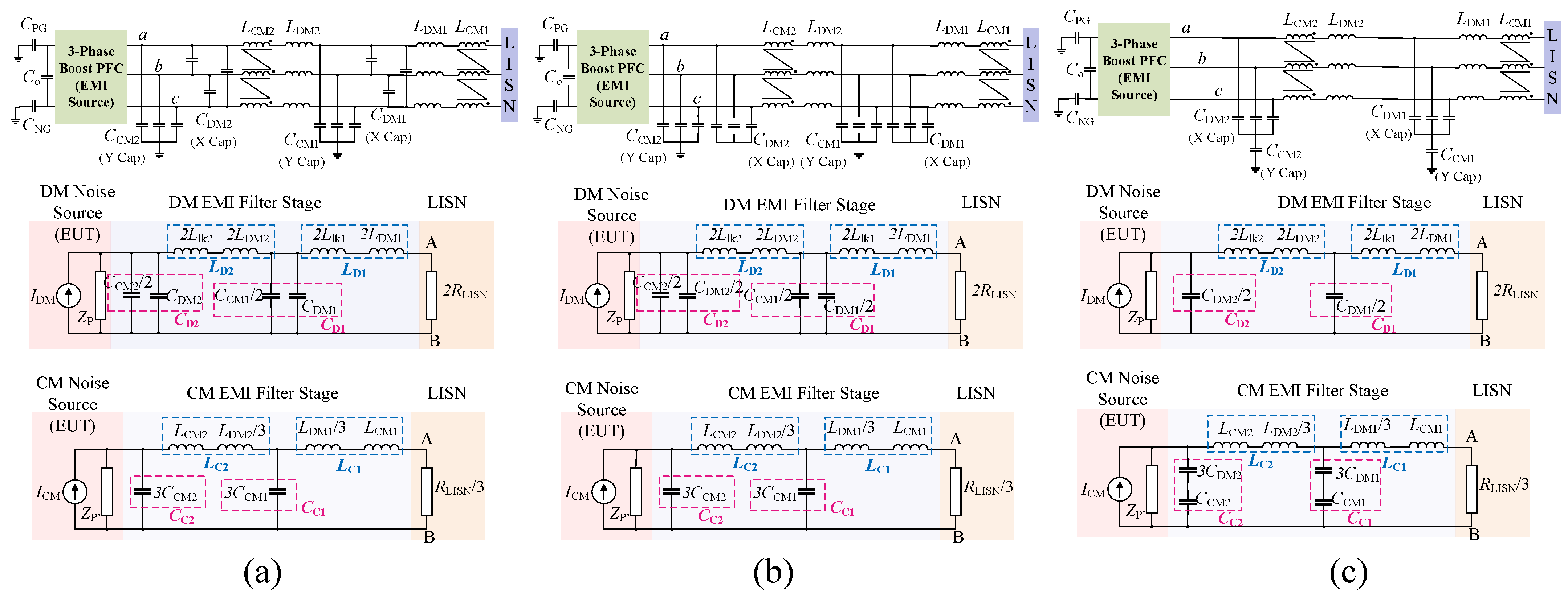
4. Synthesis of Various Three-Phase EMI Filter Structures
The conventional EMI filters in the power electronics field typically consist of one or two stages of undamped or damped LC filters. In this section, the possible options for building three-phase EMI filter stages have to be reviewed and analyzed in detail. In contrast with single-stage EMI filters, the number of possible topologies in three-phase filters is considerably larger. Furthermore, damping resistor-based compensation methods extend the number of possible topologies for the three-phase EMI filter design even further. To avoid the complexity of analysis, damping resistor utilization is kept as beyond the scope of this paper. Generally, the EMI filter consists of two types of building blocks, namely, inductor and capacitor. The number of possible arrangements for inductor elements is very small. Common mode and differential mode chokes with or without integrated structure represent two possible inductor stage topologies. On the contrary, there can be different possibilities of arrangements for the capacitor stages, based on several connection types. The primary connection types for the capacitors in a three-phase EMI filter are:
X-capacitors (DM stage) placed between phases
X-capacitors (DM stage) connected to a star node
Y-capacitors placed between the star node and the protective earth (integrated CM and DM stage capacitors)
Based on the connection types mentioned above, we have developed three distinct possible EMI filter structures that can be employed to attenuate the noise level of our CUT.
Figure 5 depicts the three different two-staged EMI filter structures (Filter Structure 1 to Filter Structure 3) under study and their corresponding DM and CM equivalent circuits. In each of the two-staged filter structures, there are a total of six decoupled DM line inductors (
while the CM stage comprises of a set of two CM chokes. The filter structure 1 has six phase–phase X capacitors, forming the DM stage, connected in a delta fashion, whereas the DM stage of the filter structure 2 has six line–line X capacitors connected in a start fashion. The CM stage for both the filter structures 1 and 2 is formed by six line-ground Y capacitors. It is noteworthy that for the phase–phase connection, X capacitors with a higher voltage rating (ph–ph voltage = 230
= 400 V applied across each capacitor) must be used compared to line–line connected capacitors.
On the other side, the filter structure 3 has an integrated DM and CM capacitor stage formed by six line–line X capacitors placed in a star fashion and two Y capacitors connected between the star point and the ground. The component count in this filter structure is less than the other two structures. Furthermore, in this topology, the values of X and Y capacitors influence both the CM and DM filter stages.
The design of the filters through deriving the DM and CM filter stage attenuation equations for each of the filter structures are separately presented below.
4.1. DM Filter Design
In order to synthesize the DM filter stage parameters, the per phase DM equivalent circuits of the filter structures, as presented in
Figure 5, need to be examined. In all the three DM equivalent filter circuits, the CUT DM noise source is modeled as a current source
with a parallelly connected impedance
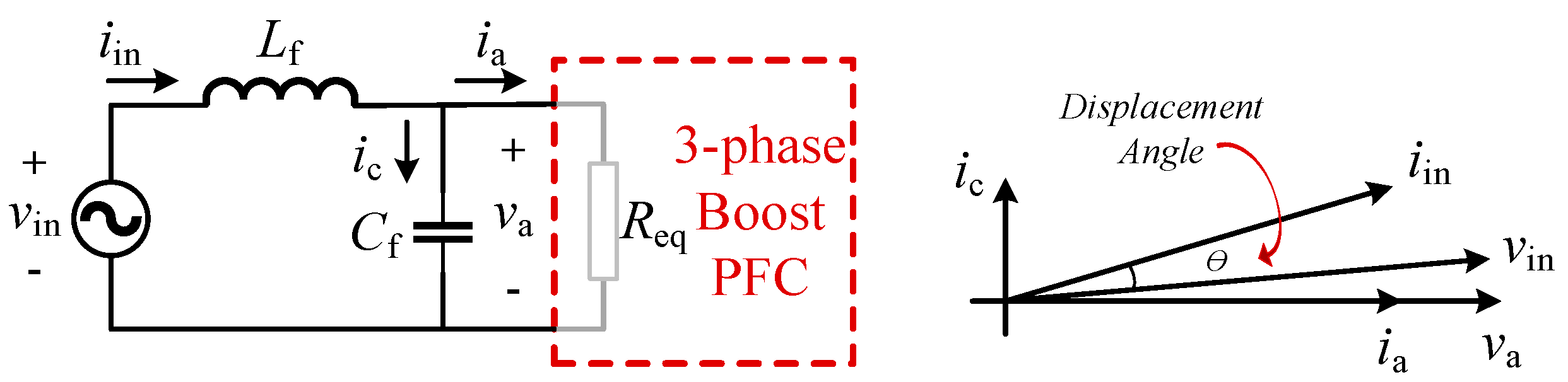
, which essentially represents the PWM converter. Moreover, for the sake of simplicity in analyzing the circuits, we have considered the assumption: the input-side impedance offered by both Y-capacitances and the effective series inductive path is considerably higher than the total line impedance stabilization network (LISN) in order to complete a DM noise path, i.e.,
, where
and
signify LISN impedance, leakage inductances for the CM chokes
and
per phase, respectively. Considering this assumption, the per phase DM equivalent circuit is deduced for all the three filter topologies. The equivalent circuit comprises two back-to-back connected LC filter stages with the DM inductors
and
(
,
and capacitors
and
, the values of which for different filter topologies are given below.
Filter Structure 1: and
Filter Structure 2: and
Filter Structure 3: and
Hence, based on the above-mentioned assumption and the derived circuit parameter values, the cut-off frequencies for different DM filter structures can be expressed in the generalized form:
and
. Thus, the total attenuation offered by the total DM filter stage at a design frequency,
, can be determined using (18).
To attain the smallest filter volume, the DM filter components of each filter stage should be equal [
10], i.e.,
LDM1 =
LDM2;
CDM1 =
CDM2 and
LD1 =
LD2 =
LD;
CD1 =
CD2 =
CD. Considering this, the DM LC filter attenuation considering
Nf filter stages can be expressed as:
which should satisfy the required amount of noise attenuation at
noise frequency,
.
4.2. CM Filter Design
Like the DM filter stage, the per phase CM equivalent circuits of the EMI filter topologies are obtained in
Figure 5. Here, the CM noise source present inside the CUT is represented as a noise current source
with a parallel impedance
. While analyzing the circuits, a critical assumption is that the equivalent CM impedance should be large enough compared to the LISN impedance, i.e.,
. It is further assumed that all the phases contain symmetric CM noise current distribution. Keeping the stated assumptions in mind, the per phase CM equivalent circuits are deduced for all of the three filter topologies. All the CM equivalent circuits comprise similar structures of two back-to-back connected LC filter stages with the inductors
and
(
;
and capacitors
and
, the values of which for different filter topologies are presented here.
Filter Structure 1: and
Filter Structure 2: and
Filter Structure 3: and
This two-staged CM LC filter, having two corner frequencies at and , generates combined total filter attenuation of to a noise of frequency.
For a
Nf staged CM EMI filter, containing same per stage components (i.e.,
LCM1 =
LCM2;
CCM1 =
CCM2 and
LC1 =
LC2 =
LC;
CC1 =
CC2 =
CC), it can provide an attenuation as expressed in (20).
5. Filter Volume Optimization and Volumetric Comparison between the EMI Filter Structures
In this section, a generalized optimization of the EMI filter size is performed through development of volumetric cost function models of the filter components, particularly for the DM stage, as it contributes to most of the filter volume. It is evident from (17) that multiple combinations of the LC parameter values along with a different number of filter stages for the DM filter will satisfy the attenuation requirement criteria. This opens up the possibility to optimally choose the filter parameters, LD, CD and for any general EMI filter structure.
In order to start with minimizing the total DM filter volume, the basic requirement is of a quantified cost function model of the per-stage DM capacitor and inductor volume. Though the work in [
10] presents such developed volumetric models, due to involvement of less component related design variables, it lacks accuracy. A similar research effort has been placed in this work to determine the near accurate volumetric model of the filter components. Although, conventionally, the inductor or capacitor volume is considered to be proportional to the stored energy, here, we have come up with more accurate regression models for the filter capacitor and inductor volume, considering different combinations of the chosen decision variables: rated voltage (
V), rated current (
I), capacitance (
C), inductance (
L), a scaled factor of the stored energy (
CV2 or
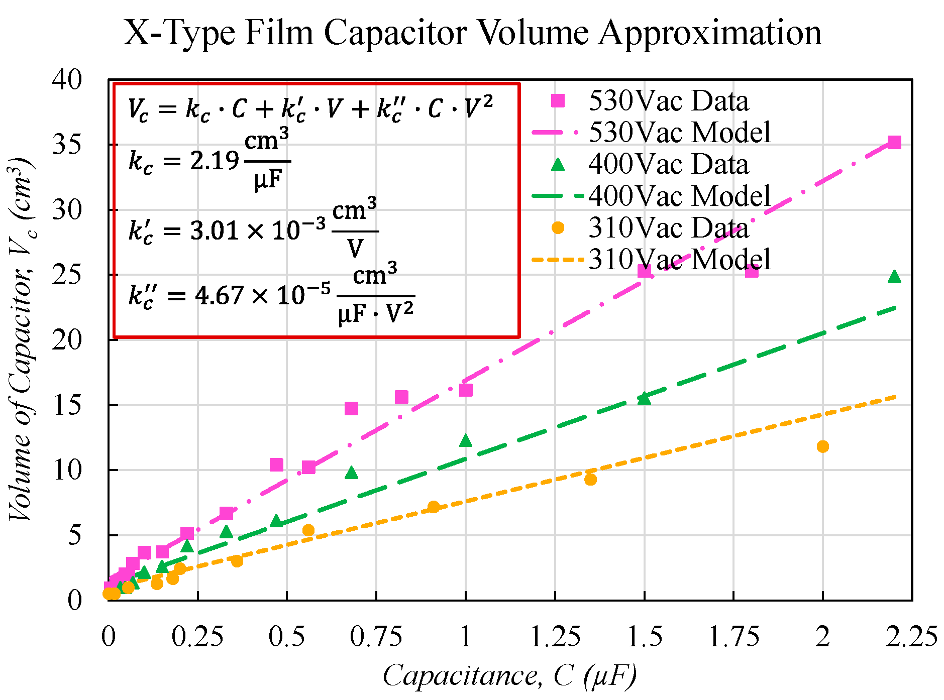
LI2) and a constant factor. Thus, the capacitor volume is presented as:
where the coefficients
,
, and
describe the proportionality of capacitor volume with the capacitance, the rated voltage and the stored energy, respectively. The values of the coefficients are determined by fitting the volumes of the commercially available Film type X-capacitors into the proposed model, as shown in
Figure 6, while applying the variance-minimization technique.
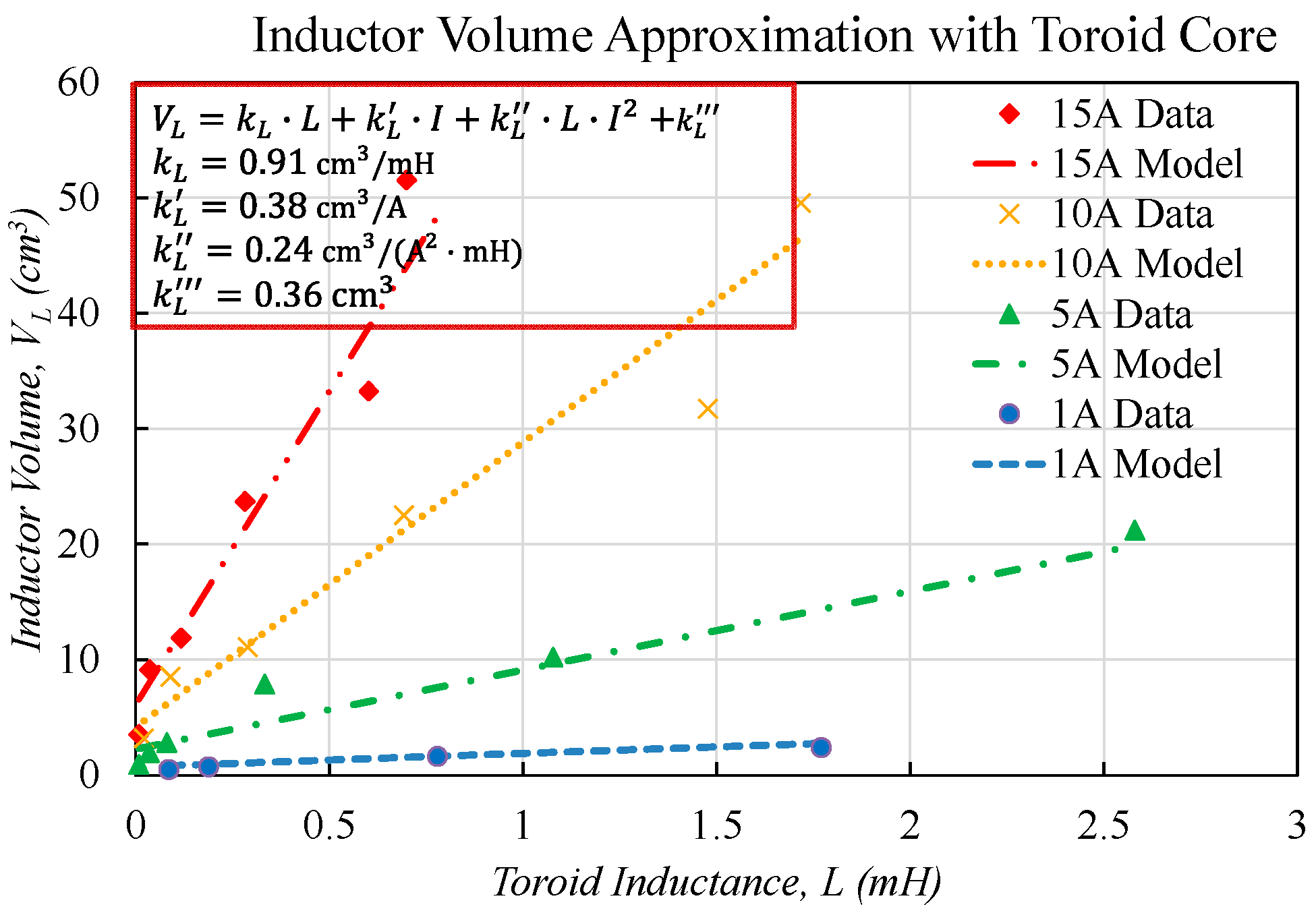
Likewise, the toroidal core filter inductor volume is found to be best quantified as:
where
,
and
represent the coefficients for the filter inductance (
L), rated current of the inductor (
I), the stored energy (
LI2) and a constant factor, respectively. The fitting of the raw inductor volume data into the proposed model is depicted in
Figure 7, which outputs the coefficient values.
Now, the DM filter volume for
Nf symmetrical filter stages can be shown as:
where
and
represent the volumes of each
LDM1 and each
CDM1, respectively. To accomplish the least filter volume, (23) needs to be minimized while satisfying the attenuation requirement constraint, given in (19). While solving these two equations, we do not consider the minimal contribution of the
CCM capacitors towards
CD due to their lower value. Using similar logic, we also ignore the contribution of the leakage inductance of the CM choke in forming the net DM inductance,
LD. While considering these assumptions, analyzing the DM equivalent circuits of the three filter structures under study, total DM filter attenuation (19) is modified as:
Now, can be expressed in terms of and for all the filter structures using (24) and (25). Putting the quantified volumetric models of and into use (as given in (21) and (22)), the total DM filter volume, given by (23), can be minimized as . This yields the optimized values of the filter components for the different filter structures.
These results show that the optimized values of the DM filter components for the Filter Structure 1 will be different than the rest of the filter topologies. Furthermore, it is found that the optimized component value does not just depend on , but it also depends upon and the rated capacitor voltages.
For the purpose of validation of the volume-optimized filter design methodology described above and to compare the filter volumes, three EMI filters comprising the three topologies under study is designed to employ in the front end of a 2.3 kW three phase boost rectifier. The optimized DM filter parameters for our designs are determined using (24)–(27) while varying the number of filter stages from 1 to 4, as shown in
Table 1. In the table, we have considered the maximum allowable displacement angle for input side PFC as 5°, which sets an upper bound to the total employable DM filter capacitance per stage (
) and thus, limits the
sample space in the volume optimization methodology. It can be inferred from the data presented in
Table 1 that for a 50 dB attenuation requirement at
of 200 kHz, all the three filter structures attain their lowest volume with two filter stages. While Filter Structure 1 achieves a minimum volume of 73.58 cm
3 with
LDM and
CDM values of 28.2 µH and 200 nF, respectively, Filter Structures 2 and 3 attain a better power density with a minimum DM filter size of 66.32 cm
3, with
LDM and
CDM values of 37.2 µH and 302.7 nF.
Finally, the volumetric optimization procedure of the DM filter stage is extended to the CM counterpart as well, and the globally optimized EMI filter volumes for the three filter topologies are mathematically determined, as presented in
Table 2. The data suggest that although the optimized DM stage filter volumes for Filter Structure 2 and 3 are found to be same, the presence of integrated CM and DM mode capacitors leads the structure 3 to reach a better total EMI filter power density, when compared to the structure 2. Hence, when compared in terms of better system volume, the Filter Structure 3 has come up as the superior to rest of the filter structures under study.
6. Experimental Results
To validate the filter design-related mathematical formulations, a proof of concept of a 2.3 kW rated three-phase boost PFC along with the EMI filter stage was designed, developed, and tested.
Figure 8 portrays the simulated DM EMI spectrum ranging from 150 kHz to 5 MHz of the converter upon application of the filter structure 2 with the optimized filter parameters. It shows that the EMI performance of the converter integrated with the EMI stage satisfied the DO-160F conducted EMI standard, with a sufficient margin of 3dB. Moreover, the EMI compliance of the fabricated experimental setup of the EMI+PFC stage was verified through
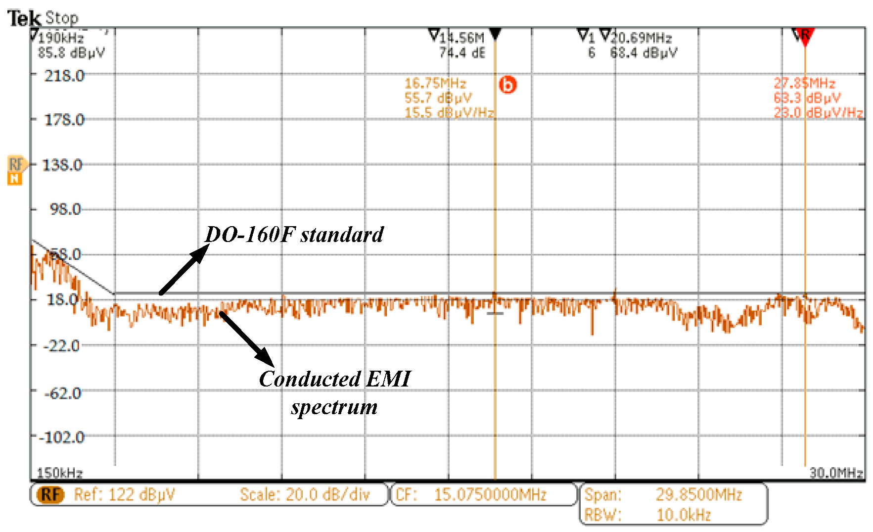
Figure 9. It demonstrates the EMI spectrum of the converter for the whole conducted EMI range from 150 kHz to 30 MHz, which achieved the DO-160F EMI standard.
In order to verify the accuracy of the developed mathematical models for filter volume optimization and to perform the volumetric comparison between different possible EMI filter structures, all of the three filter structures comprising the optimized component values, as presented in
Table 2, were fabricated and tested for EMI compliance. The fabricated Filter Structure 3 was measured to achieve a total volume of 98 cm
3, which was 16.3% and 22% less than the Filter Structure 2 and 1, respectively. Thus, these measurements aligned with our mathematically derived conclusions.
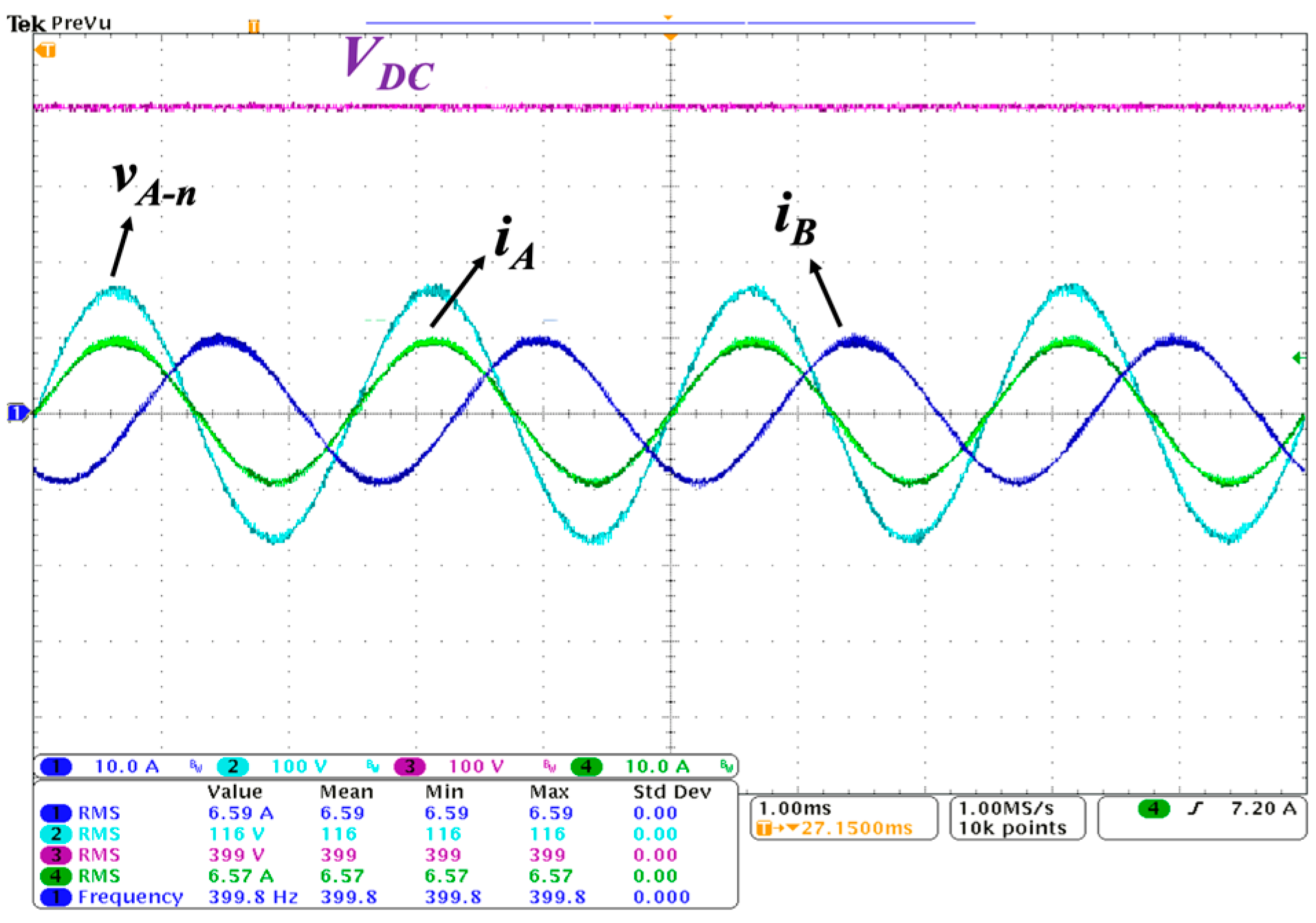
Figure 10 shows the experimental waveforms for the input phase currents
iA,
iB, phase ‘A’ voltage
vA-n and the output DC link voltage
vDC of the fabricated PFC integrated with the EMI stage. The measured data reported a THD of 4.3%, and the input power factor was 0.998. The overall efficiency of the integrated EMI and PFC stages was found to be 98.87%, while the efficiency of the standalone EMI stage was 99.5%.
7. Conclusions
This paper discussed a detailed step-by-step procedure for the development of an optimally designed EMI filter for a three-phase boost PFC converter used in EMI stringent applications, such as more electric aircrafts (MEA). A mathematical foundation for the volume optimized design of the DM and CM EMI filter stages comprising any filter structure was also developed and presented. The optimized filter parameter values were derived based on the proposed volumetric models of the filter elements, which suggested that the EMI filter volume primarily depends on multiple factors, including the noise attenuation requirement (Attreq), the filter design frequency (fD), the count of filter stages (Nf), the rated voltage for CD or Cc and the rated current for LD or Lc. In this work, the volumetric optimization methodology was applied on the three different EMI filter structures with different X and Y capacitor arrangements in order to find the best-suited filter structure for our three-phase PFC unit in terms of highest power density. Based on the analysis, for the same attenuation requirements, the filter Structure 3 achieved the smallest volume (94.8 cm3, which was 24% and 17% less than the optimized filter volumes of filter structure 1 and 2, respectively) as it benefits from its CM-DM integrated design, with only one Y-capacitor per LC filter stage, compared to three in the other two filter structures. To verify the theoretical analysis, the EMI spectrum evaluation was performed on a proof-of-concept of 2.3 kW rated AC-DC active boost PFC-EMI integrated stage. The experimental results revealed a complete agreement with the conducted EMI standard DO-160F while maintaining a sufficient margin. With the proposed EMI structure solution 2, the PFC converter maintained an efficiency of 98.87%, with an input power factor of 0.998, hence demonstrating good power quality.


