Abstract
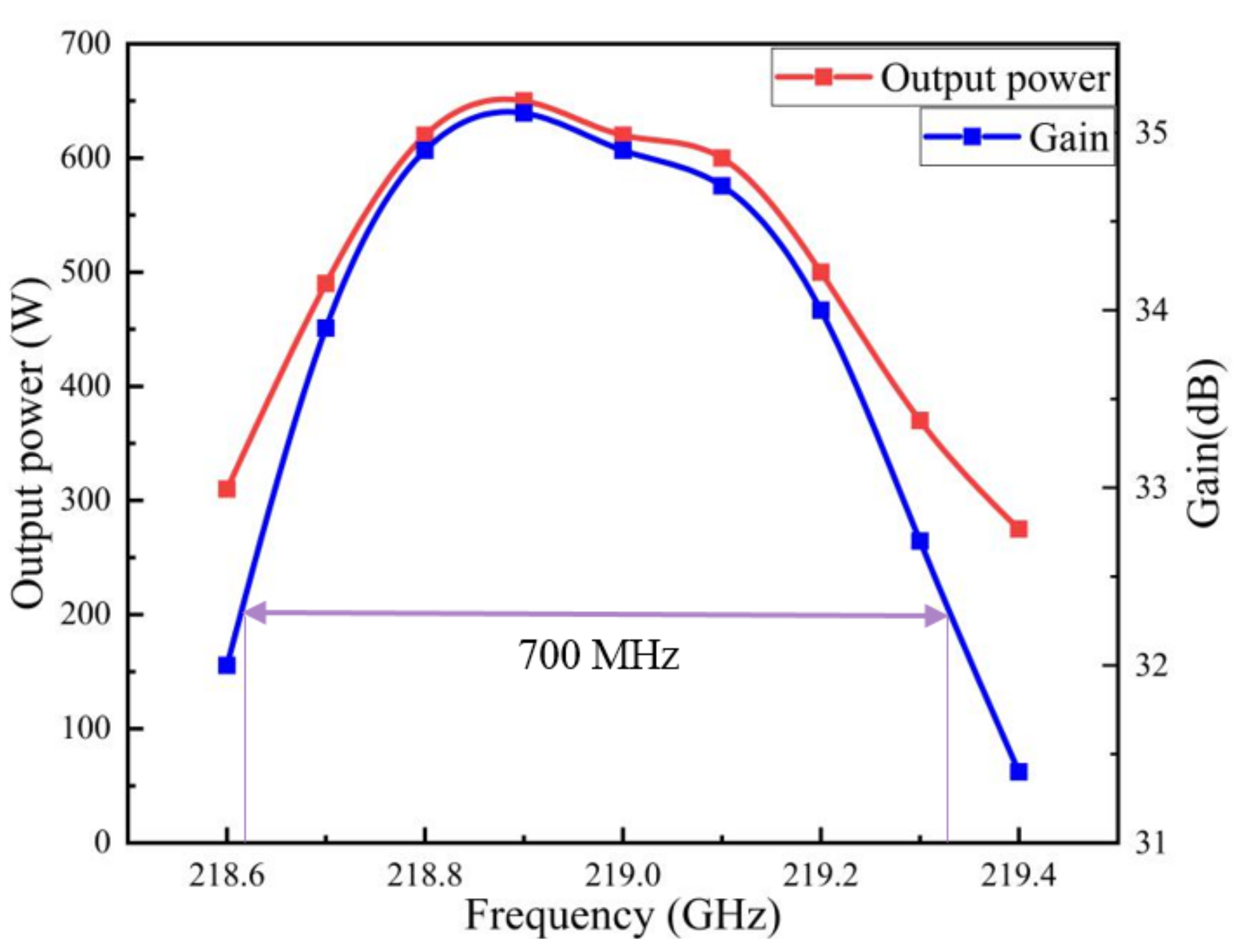
In this paper, we propose a high-order mode sheet beam extended interaction klystron (EIK) operating at G-band. Through the study of electric field distribution, we choose TM31 2π mode as the operating mode. The eigenmode simulation shows that the resonant frequency of the modes adjacent to the operating mode is far away from the central frequency, so there is almost no mode competition in our high mode EIK. In addition, by studying the sensitivity of the related geometry parameters, we conclude that the height of the coupling cavity has a great influence on the effective characteristic impedance, and the width of the gap mainly affects the working frequency. Therefore, it is necessary to strictly control the fabrication tolerance within 2 μm. Finally, the RF circuit using six barbell multi-gap cavities is determined, with five gaps for the input cavity and idler cavities and seven gaps for the output cavity. To expand the bandwidth, the stagger tuning method is adopted. Under the conditions of a voltage of 16.5 kV, current of 0.5 A and input power of 0.2 W, the peak output power of 650 W and a 3-dB bandwidth of 700 MHz are achieved without any self-oscillation.
1. Introduction
Terahertz technology has become one of the most popular technologies, and it has important applications in high-resolution imaging, medical detection, channel communication, material structure analysis and so on [1]. However, this research and development has been restricted by terahertz radiation sources, which can produce high power, high bandwidth and high efficiency and are easy to use. Therefore, the research of terahertz sources is urgent. An extended interaction klystron (EIK) is a potential terahertz source which was proposed by Chodorow and Wessel-Berg in the 1960s [2,3]. It combines the high gain of klystron with the broad bandwidth TWT, which shortens the length of the circuit [4]. Moreover, the EIK adopts a multi-gap resonator which improves the characteristic impedance and the gain bandwidth [5]. However, due to the limitation of the high frequency and precision structures, the development of EIKs is still very slow. Nowadays, with the development of science and the research of terahertz technology, EIKs are undoubtedly put forward in the direction of high power, a high frequency and a wide bandwidth with the urgent demand [6].
Many institutions in China and abroad have conducted in-depth research on EIKs. CPI (Communications & Power Industries, Canada) has been studying EIKs for many years, which in the millimeter wave band have been very mature, with their products being developed for various equipment [7,8]. In recent years, their research on EIKs in the terahertz band has also made great progress. CPI has developed EIKs with a peak output power of 52 W and operating frequency of 220 GHz [9]. In addition, the NRL (Naval Research Lab, Washington, DC, USA) first reported on the sheet beam EIK in 2007 [10]. The G-band sheet beam EIK designed by NRL has 453 W of output power under the conditions of a voltage of 16.5 kV and a current of 0.52 A [11]. The research of EIKs in China started late, and now it is mainly focused on the W-band and G-band [12,13]. The Ka-band EIK has been developed by the Institute of Electronics at the Chinese Academy of Sciences, with an average output power of 355 W and 3-dB bandwidth of 410 MHz under an operating voltage of 9 kV and current of 0.15 A [14]. Recently, they developed a W-band EIK with a maximum output power of 1.5–3 kW. Xi’an Jiaotong University designed an EIK operating in TM31 mode that works in the G-band with an output power of 60 W and instantaneous bandwidth of 300 MHz [15]. In short, the research of terahertz EIKs in China needs to be further improved.
In this paper, we aim to design a high-order mode structure with an output power of 500 W and 3-dB bandwidth of 600 MHz with the sheet beam EIK operating in TM31 mode. Compared with the traditional EIK using the fundamental mode, the high-order mode can increase the size of the structure, thus reducing the difficulty of processing and enhancing the power density. Aside from that, the current density is also reduced, so the space charge effect can be reduced and the breakdown does not occur easily. Compared with the structure in [15], our structure uses a sheet beam instead of a circular electron beam to reduce the current density and the difficulty of processing, and the simulation results show that the output power and bandwidth of our EIK are much higher. Through design, analysis and optimization, we obtain an input/output cavity and an idler cavity with a resonance frequency of about 220 GHz, uniform electric field distribution and high characteristic impedance. Considering the machining error, we study the multi-gap cavity and get the allowable range for error. In this paper, the designed sheet beam EIK consists of six multi-gap cavities of the barbell type. In addition, to expand the bandwidth, we use stagger tuning technology. To get a better output characteristic, we have conducted detailed analysis on the input power, voltage and current as well as our magnetic field. Finally, under the condition of an input power of 0.2 W, voltage of 16.5 kV, current of 0.5 A and magnetic field of 0.5 T, 650 W of output power and 700 MHz at a 3-dB bandwidth are obtained, which are the milestones for the generation of high-output power in the G-band.
2. Consideration of High-Order Mode Structure
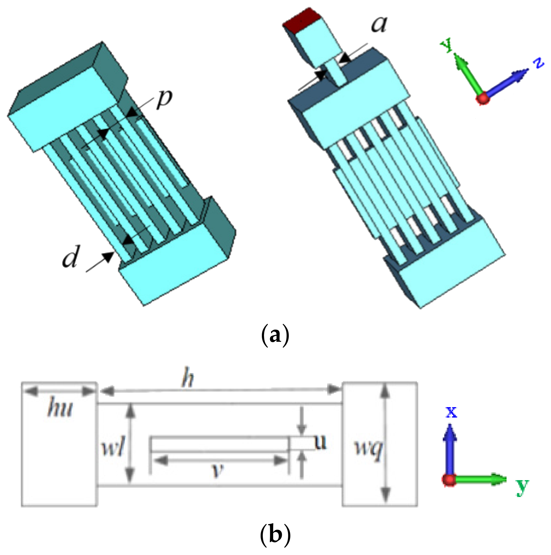
In this paper, a high-order mode coupled cavity with periodic arrangement gaps is designed. The 3D model of the idler cavity and output cavity are shown in Figure 1a using the scheme of a sheet beam (aspect ratio is 10). Figure 1b shows the cross-sections in the xy plane, where the period between the gaps is p, the length of the gap in x direction is d in the z-axis, the width and height of the gap are wl and h, respectively, the width and height of the beam tunnel are v and u, respectively, and the width and height of the coupling cavities are wq and hu, respectively.

Figure 1.
Schematic of the multiple gap cavity for the EIK. (a) A 3D model of the idler cavity and output cavity. (b) A cross-section in the xy plane.
We chose TM31 mode as the operating mode, which can be compared with the traditional scheme of the fundamental mode TM11 in Figure 2. On the one hand, the electric field of TM11 mode is stronger near the upper and lower coupling cavity, and the electric field at the center gap is a little weaker, as shown in Figure 2a, which was not suitable for the sheet beam we used. In addition, with the same dimension of the TM31 mode cavity working at 220 GHz, the resonance frequency of the TM11 mode is about one third, which is far away from the G-band. However, the electric field of the TM31 mode is mainly distributed in the middle, and the electric field is stronger, as shown in Figure 2b. Therefore, the TM31 mode is more beneficial for sheet beam interaction. On the other hand, the dimensions of the structure designed using TM31 mode are larger, which makes it less difficult to fabricate later.

Figure 2.
Electric field distribution of (a) fundamental TM11 mode and (b) high-order TM31 mode.
3. Cavity Design and Eigenmode Simulation
The distance between two adjacent gaps is p, as shown in Figure 1a, and it can be figured out from Equations (1) and (2) [16]. U0 and f0 are the operating voltage in kV and frequency in Hz, respectively, c is the speed of light and ve and vp are the electron velocity and phase velocity, respectively. Using these formulas, we can roughly calculate the initial parameters we need, and then the structure is further optimized by three-dimensional CST software [17]:
p = ve/f0
As a figure of merit, the effective characteristic impedance (R/Q)·M2 is chosen to evaluate the beam–wave interaction ability of the EIK [18]. In the expression of (R/Q)·M2, R/Q and M are the characteristic impedance and coupling coefficient, respectively [19]:
where Ez, Ws, ω, and βe are the axial electric field, total stored energy, angular frequency and electronic wave number, respectively.
Through a large amount of simulation, the optimized geometry parameters of the idler cavity with five gaps are given in Table 1, which corresponds with Figure 1. Then, the electric field distribution of the five-gap idler cavity is shown in Figure 3. As can be seen from the Figure 3a, the phase difference between the adjacent gaps is 2π, and the electric field distribution accords with the TM31 mode. Additionally, the electric field distribution is mainly concentrated in the upper and lower coupling cavities and the middle of the gap. The electron channel is located in the region of a strong electric field in the middle of the gap, which enhances the beam–wave interaction.

Table 1.
Optimized parameters of idler cavity.
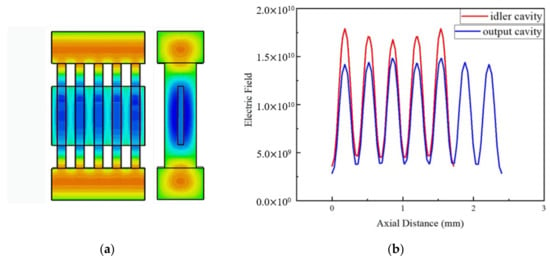
Figure 3.
Electric field distribution for the 5-gap idler cavity and 7-gap output cavity. (a) Electric field distribution and mode pattern for 5-gap idler cavity. (b) Axial electric field distribution for idler and output cavities.
For the seven-gap output cavity, the dimensions and location of the coupling hole are important factors, affecting the electric field distribution and performance, especially Qe, as shown in Figure 1a. Different widths of the coupling hole and different positions of the coupling hole were studied and, it was found that when the width was 0.2 mm and the coupling hole was located in the middle of the upper surface of the coupling cavity, the electric field distribution of the output cavity was strong and uniform, and the Qe value was the most appropriate for the EIK. Figure 3b shows the axial electric field distribution. Whether in the idler cavity or the output cavity, the electric field should be evenly distributed. Aside from that, the electric field in the gap is stronger, while between the adjacent gaps it is weak, which provides the possibility of getting good output results. Table 2 gives the performance values of the operating mode and its adjacent modes. From the table, we can see that only (R/Q)·M2 of the operating mode near 220 GHz is high enough and reasonable for beam–wave interaction. Moreover, the frequency interval between the operating mode and the adjacent modes is very large, so there is almost no possibility for mode competition in the EIK.

Table 2.
The performance of the operating mode and its adjacent modes.
4. Sensitivity Analysis for the Cavity
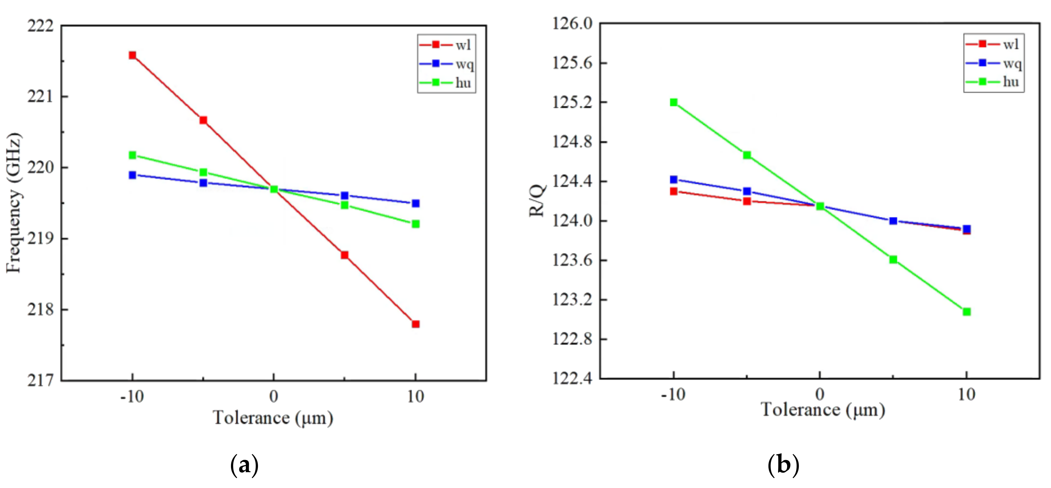
In the mm wave and THz frequency band, devices are compact and miniaturized. Thus, small changes in dimensions may have a great impact on device performance. However, errors are inevitable in manufacturing, so an acceptable fabrication tolerance should be considered thoroughly. Figure 4 shows the influence of manufacturing error on the frequency and R/Q of an EIK with several typical geometry dimensions, (e.g., wl, wq and hu). It can be seen from Figure 4a that the change of wl has the greatest influence on the frequency. The 2-μm changes in wl will cause a frequency variation of about 300 MHz. The width and height of the coupling cavity (wq and hu) have little effect on the frequency, especially wq. Therefore, wl can be used to adjust the frequency in a large range, and hu can be used to adjust the frequency in a small range. From Figure 4b, it can be seen that the change of wl and wq has little effect on the characteristic impedance, while hu has a little greater effect on the characteristic impedance. Therefore, in the structural design, wl can be adjusted to obtain the desired resonance frequency, and it can also be appropriately increased to improve the characteristic impedance. If high characteristic impedance is required, the hu should be adjusted. To sum up, if the fabrication tolerance is controlled within 2 μm, the output characteristics of the EIK will be less affected with good performance. At present, the advanced micro machining technology can provide very high machining accuracy within 2 μm, such as DIRE, UV-LIGA, WEDM and Nano-CNC. In addition, the key technique of the dynamic tuning structure must be used for each multi-gap cavity of the EIK [20], which can definitely adjust the cavity frequency to the right working condition for the optimization of output properties.
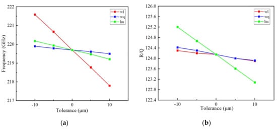
Figure 4.
Influence of the fabrication tolerance of Δwq, Δwl and Δhu on the high frequency characteristics: (a) sensitivity of frequency and (b) sensitivity of R/Q.
5. Beam–Wave Interaction Simulation
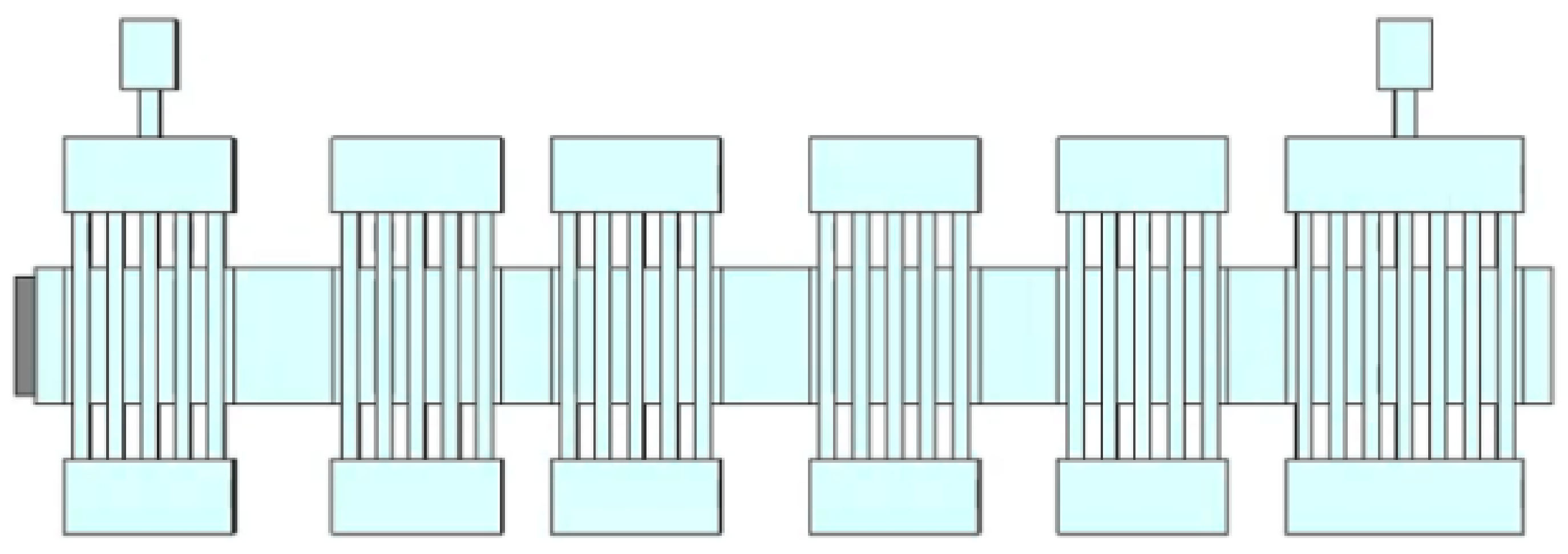
Following the multi-gap cavity optimization, the beam–wave interaction system of the EIK should be analyzed thoroughly. Figure 5 shows the complete beam–wave interaction model of a six-cavity EIK we designed with CST three-dimensional software, the input cavity and the idler cavity adopted five gaps, and the output cavity adopted seven gaps. We studied the length of the drift tube between each cavity and determined the appropriate values with more analysis. In order to extend the bandwidth for our multi-gap and multi-cavity EIK, the traditional stagger tuning method was adopted in our simulation, which has been widely used for the design of a multi-cavity klystron [21,22,23]. The high-frequency characteristic parameters of each cavity were optimized, and they are listed in Table 3. By adjusting the value of wq, the resonant frequency of the idler cavity could be changed a little for the stagger tuning requirements, and then the best matching value of each cavity could be optimized for the beam–wave interaction analysis for our EIK.
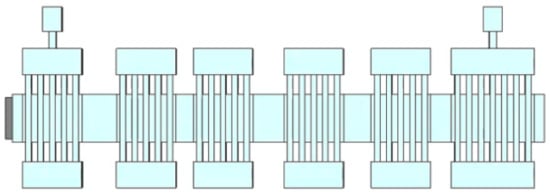
Figure 5.
A 3D PIC simulation model of the complete EIK structure in CST.

Table 3.
Optimized parameters of each cavity for the EIK.
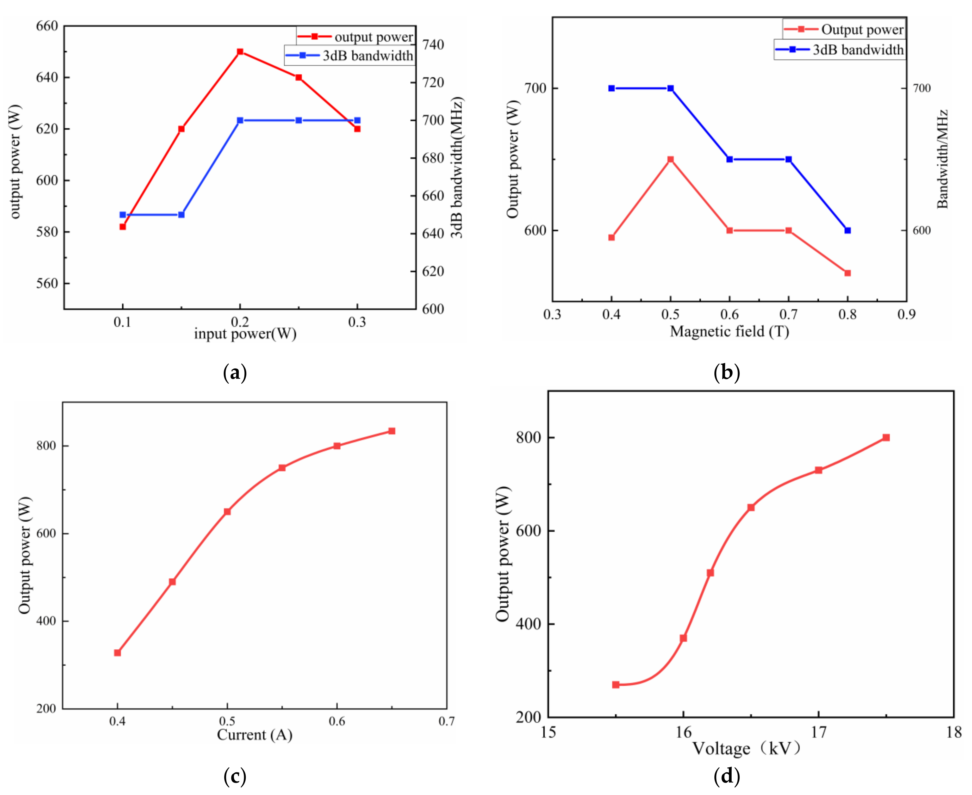
For thorough beam–wave interaction analysis of the G-band EIK, optimization of the key parameters was performed with only one parameter change as shown in Figure 6. The relationship between the output power and 3-dB bandwidth with the input power has been given in Figure 6a. It was indicated that the output power increased first and then decreased with the increase in input power, and it reached the maximum value when the input power was 0.2 W. As the input power increased, the 3-dB bandwidth first increased and then tended to be stable. In addition, the gain decreased with the increase in the input power. Therefore, to obtain a high output power at a 3-dB bandwidth, the input power should not be too large. Therefore, we used 0.2 W as the optimized input power. With the same method, the magnitude of the magnetic field affecting the beam–wave interaction was analyzed. Figure 6b shows the relationship between the output power and magnetic field. When the magnetic field was small, as the magnetic field increased, the electron was well bound in the channel, the beam–wave interaction enhanced, and the output power would be increased. When the magnetic field was 0.5 T, the output power and bandwidth were at their maximums of 650 W and 700 MHz, respectively. Therefore, the 0.5-T magnetic field could be selected for our EIK.
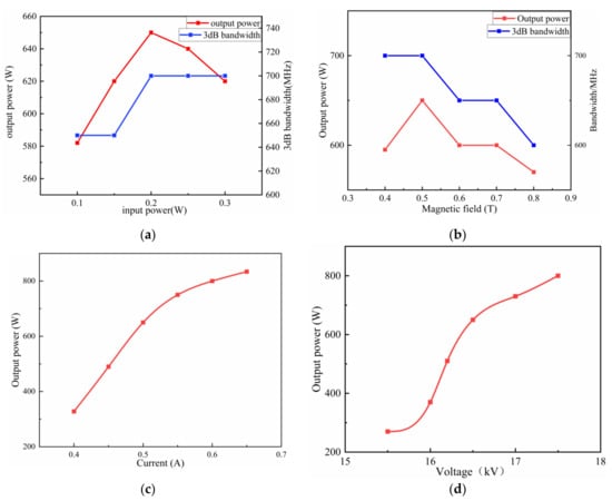
Figure 6.
The variation of the output power and bandwidth with typical parameters. (a) The output power and 3-dB bandwidth variation with the input power, where the current (0.5 A), voltage (16.5 kV) and magnetic field (0.5 T) remain unchanged. (b) The output power and 3-dB bandwidth variation with the magnetic field, where the current (0.5 A), voltage (16.5 kV) and input power (0.2 W) remain unchanged. (c) The output power variation with the current, where the voltage (16.5 kV), magnetic field (0.5 T) and input power (0.2 W) remain unchanged. (d) The output power variation with the voltage, where the current (0.5 A), input power (0.2 W) and magnetic field (0.5 T) remain unchanged.
Figure 6c shows the relationship between the output power and beam current. It can be seen from the figure that as the current increased, the output power and gain increased. However, if the current was too large, although the output power would be improved, the beam focus could be more difficult, and it would also bring instability for the beam–wave interaction for the EIK. Therefore, the current of the amplifier should not be too large, and 0.5 A was selected here, with the corresponding current density being 255 A/cm2. Figure 6d shows the relationship between the output power and voltage. With the increase in voltage, the output power also increased. If the voltage increased further, the increase in the output power would become smaller, but the voltage should not be too high. When the voltage value was small, the output was small, but the output characteristics were stable, and the time for the stable output power was short. When the voltage was too high, although the output power increased, the beam–wave interaction synchronization would be destroyed, and the output became unstable. There is a typical phenomenon in which the output power increases first, then decreases, and then it tends to be stable. As such, it will take a long time to stabilize the EIK. Thus, in this research work, the input voltage could be optimized to 16.5 kV for good performance.
After the above optimization, the structure parameters and output characteristics of the EIK were determined thoroughly. As for the results, Figure 7a shows the peak output signal at a resonant frequency of 218.9 GHz, voltage of 16.5 kV, current of 0.5 A and magnetic field of 0.5 T. It can be seen from the figure that at the beginning, the output signal gradually increased, and it soon reached the maximum value at 2.5 ns and then remained stable later. Figure 7b shows the phase space portrait of the electron energy along with the axial distance. It can be seen that in the first few cavities, due to the weak modulation effect, the energy of the electron beam changed little and fluctuated around 16 KeV, while with the enhancement of the modulation effect of the latter several cavities, the energy conversion gradually increased, and when it came to the output cavity, most electrons decelerated while a few electrons accelerated. Thus, much of the energy of the electrons would be released effectively. Figure 7c shows the bunching of the electron beam. It can be seen that the bunching effect of the electron beam from the input cavity to the output cavity was gradually enhanced, reaching its maximum in the output cavity, indicating that the electron beam had good interaction with the electromagnetic wave. Figure 7d is the frequency spectrum of the input and output signals, which shows that the amplified signal only had a peak value at 218.9 GHz, which was the same as the input frequency. In addition, the peak value of the output signal was 35 dB higher than the input signal. This shows that there was not any mode competition in the structure, and the input signal was amplified well.
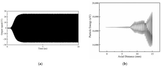
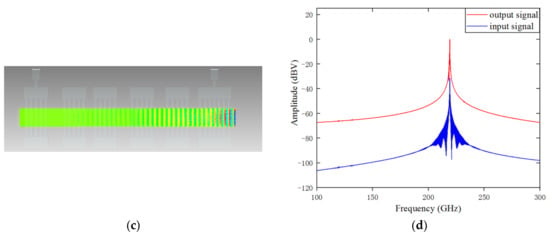
Figure 7.
Output characteristics of the EIK at a frequency of 218.9 GHz: (a) Output signal versus time; (b) phase space portrait of the particle energy distribution; (c) beam bunching sketch; and (d) frequency spectrum of the input and output signals.
Figure 8 shows the relationship between the output power and frequency for our designed EIK. Under the conditions of a voltage of 16.5 kV, current of 0.5 A, focus magnetic field of 0.5 T and input current of 0.2 W, the maximum output power could reach 650 W at the frequency of 218.9 GHz. If the resonance frequency was increased or decreased, the output power would decrease gradually. Thus, the 3-dB bandwidth of 700 MHz could be achieved successfully, which was very high for a high-order mode and sheet beam EIK. Additionally, the RF efficiency of our EIK was 7.9%, and when the input power was zero, the output power of the EIK was very small, being almost zero, which shows that our structures had good suppression of self-excited oscillation, which undoubtedly made our G-band EIK have stable output performance for the beam–wave interaction and reliable output performance.
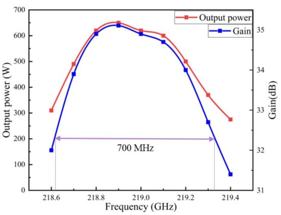
Figure 8.
Output power and gain versus frequency.
The characteristic parameters of the high-order mode and fundamental mode are listed in Table 4. Compared with the circular beam EIK scheme, the sheet beam EIK with high-order mode could increase the cavity size, which reduced the difficulty of processing and also reduced the current density, so the space charge effect could be reduced. Aside from that, it could further improve the power and expand the bandwidth. Thus, our EIK with high-order mode is a good choice for high-power terahertz radiation sources [24].

Table 4.
The characteristic parameters of the high-order mode EIK and fundamental mode EIK.
6. Conclusions
We designed a sheet beam EIK structure working in the high-order mode TM31 at the G-band. This can help to increase the operation frequency with the same size of the cavity structure compared with the fundamental mode. Meanwhile, the overviewed scheme in this paper may reduce the beam current density using its big beam size and obtain a high output power and wide bandwidth. The high frequency characteristics of the multi-gap cavity were analyzed, simulated and optimized thoroughly. By adopting the stagger tuning method and six resonant cavities, we obtained good performance with a 650-W output power and 700-MHz 3-dB bandwidth with good stability. Thus, the designed physical model of our high-order mode EIK can be a good engineering choice to fabricate practical and compact radiation sources at the terahertz band in the future.
Author Contributions
Writing—original draft preparation, S.L.; writing—review and editing, S.L. and C.R.; methodology, S.L. and F.Z.; software, S.L. and F.Z.; data curation, S.L., F.Z. and P.W.; validation, F.Z. and C.R.; investigation, Y.S. and C.R.; supervision, C.R.; project administration, C.R. All authors have read and agreed to the published version of the manuscript.
Funding
This research was funded by the National Natural Science Foundation of China, grant number 61831001.
Data Availability Statement
Data is contained within the article.
Acknowledgments
The authors would like to thank J. Feng from the Vacuum Electronics National Laboratory of the Vacuum Electronics Research Institute in Beijing, China for his sincere support for the research works in this paper.
Conflicts of Interest
The authors declare no conflict of interest.
References
- Liu, W.; Zhang, R.; Wang, Y.; Ruan, C.; Liu, P. Analysis of a two-section folded waveguide of extend interaction oscillator. In Proceedings of the 2011 IEEE International Vacuum Electronics Conference (IVEC), Bangalore, India, 21–24 February 2011; pp. 231–232. [Google Scholar] [CrossRef]
- Chodorow, M.; Wessel-Berg, T. A high-efficiency klystron with distributed interaction. IRE Trans. Electron Devices 1961, 8, 44–55. [Google Scholar] [CrossRef]
- Chodorow, M.; Kulke, B. An extended-interaction klystron: Efficiency and bandwidth. IEEE Trans. Electron Devices 1966, ED-13, 439–477. [Google Scholar] [CrossRef]
- Booske, J.H.; Dobbs, R.J.; Joye, C.D.; Kory, C.L.; Neil, G.R.; Park, G.-S.; Park, J.; Temkin, R. Vacuum Electronic High Power Terahertz Sources. IEEE Trans. Terahertz Sci. Technol. 2011, 1, 54–75. [Google Scholar] [CrossRef]
- Zhang, C.; Ruan, C.; Wang, S.; Yang, S. High-power extended-interaction klystron with ladder-type structure. J. Infrared Millim. Waves 2015, 34, 307–313. [Google Scholar]
- Pasour, J.; Wright, E.; Nguyen, K.T.; Balkcum, A.; Wood, F.N.; Myers, R.E.; Levush, B. Demonstration of a Multikilowatt, Solenoidally Focused Sheet Beam Amplifier at 94 GHz. IEEE Trans. Electron Devices 2014, 61, 1630–1636. [Google Scholar] [CrossRef]
- Roitman, A.; Horoyski, P.; Hyttinen, M.; Steer, B. Wide bandwidth, high average power EIKs drive new radar concepts. In Proceedings of the Abstracts, International Vacuum Electronics Conference 2000 (Cat. No.00EX392), Monterey, CA, USA, 2–4 May 2002. [Google Scholar] [CrossRef]
- Horoyski, P.; Berry, D.; Steer, B. A 2 GHz Bandwidth, High Power W-Band Extended Interaction Klystron. In Proceedings of the 2007 IEEE International Vacuum Electronics Conference, Kitakyushu, Japan, 15–17 May 2007; pp. 1–2. [Google Scholar] [CrossRef]
- Hyttinen, M.; Roitman, A.; Horoyski, P.; Dobbs, R.; Sokol, E.; Berry, D.; Steer, B. A compact, high power, sub-millimeter-wave Extended Interaction Klystron. In Proceedings of the 2008 IEEE International Vacuum Electronics Conference, Monterey, CA, USA, 22–24 April 2008; p. 297. [Google Scholar] [CrossRef]
- Nguyen, K.T.; Pershing, D.; Wright, E.L.; Pasour, J.; Calame, J.; Ludeking, L.; Rodgers, J.; Petillo, J. Sheet-Beam 90 GHz and 220 GHz Extend-Interaction-Klystron Designs. In Proceedings of the 2007 IEEE International Vacuum Electronics Conference, Kitakyushu, Japan, 15–17 May 2007; pp. 1–2. [Google Scholar] [CrossRef]
- Nguyen, K.T.; Pasour, J.; Wright, E.L.; Pershing, D.E.; Levush, B. Design of a G-band sheet-beam Extended-Interaction Klystron. In Proceedings of the 2009 IEEE International Vacuum Electronics Conference, Rome, Italy, 28–30 April 2009; pp. 298–299. [Google Scholar] [CrossRef]
- Xing, J.; Feng, J. Millimeter Wave Extended Interaction Device. Vac. Electron. 2010, 33–37. [Google Scholar] [CrossRef]
- Ruan, C.-J.; Wang, S.-Z.; Han, Y.; Zhang, X.-F.; Chen, S.-Y. The electron optics system and beam-wave interaction for novel W-band sheet beam klystron. J. Infrared Millim. WAVES 2012, 31, 510–516. [Google Scholar] [CrossRef]
- Zhong, Y.; Wang, Y.; Zhang, Y. Design of Ka-band extended interaction klystron. High Power Laser Part. Beams 2014, 26. [Google Scholar] [CrossRef]
- Wang, D.; Wang, G.; Wang, J.; Li, S.; Zeng, P.; Teng, Y. A high-order mode extended interaction klystron at 0.34 THz. Phys. Plasmas 2017, 24, 023106. [Google Scholar] [CrossRef]
- Chen, S.; Ruan, C.; Yong, W.; Zhang, C.; Zhao, D.; Yang, X.; Wang, S. Particle-in-Cell Simulation and Optimization of Multigap Extended Output Cavity for a W-Band Sheet-Beam EIK. IEEE Trans. Plasma Sci. 2013, 42, 91–98. [Google Scholar] [CrossRef]
- CST Corp. CST PS Tutorial. Darmstadt, Germany. Available online: http://www.cst-china.cn (accessed on 30 July 2020).
- Shin, Y.; Park, G.; Scheitrum, G.; Caryotakis, G. Circuit analysis of Ka-band extended interaction klystron. In Proceedings of the 4th IEEE International Conference on Vacuum Electronics, Seoul, Korea, 28–30 May 2003; pp. 108–109. [Google Scholar] [CrossRef]
- Gilmour, A.S.; Ebrary, I. Klystrons, Traveling Wave Tubes, Magnetrons, Crossed-Field Amplifiers, and Gyrotrons; Artech: London, UK, 2011; pp. 304–307. [Google Scholar]
- Golde, H. A stagger-tuned five-cavity klystron with distributed interaction. IRE Trans. Electron Devices 1961, 8, 192–193. [Google Scholar] [CrossRef]
- Symons, R.; Vaughan, R. The linear theory of the Clustered-Cavity Klystron. IEEE Trans. Plasma Sci. 1994, 22, 713–718. [Google Scholar] [CrossRef]
- Li, R.; Ruan, C.; Zhang, H.; Haq, T.U.; He, Y.; Shan, S. Theoretical Design and Numerical Simulation of Beam-Wave Interaction for $G$ -Band Unequal-Length Slots EIK With Rectangular Electron Beam. IEEE Trans. Electron Devices 2018, 65, 3500–3506. [Google Scholar] [CrossRef]
- Li, R.; Ruan, C.; Li, S.; Zhang, H. G-band Rectangular Beam Extended Interaction Klystron Based on Bi-Periodic Structure. IEEE Trans. Terahertz Sci. Technol. 2019, 9, 498–504. [Google Scholar] [CrossRef]
- Li, R.; Ruan, C.; Zhang, H. Design and optimization of G-band extended interaction klystron with high output power. Phys. Plasmas 2018, 25, 033107. [Google Scholar] [CrossRef]
Publisher’s Note: MDPI stays neutral with regard to jurisdictional claims in published maps and institutional affiliations. |
© 2021 by the authors. Licensee MDPI, Basel, Switzerland. This article is an open access article distributed under the terms and conditions of the Creative Commons Attribution (CC BY) license (https://creativecommons.org/licenses/by/4.0/).

