Article

Design of Wideband Antenna Array with Dielectric Lens and Defected Ground Structure

1
State Key Laboratory of Reliability and Intelligence of Electrical Equipment, Hebei University of Technology, Tianjin 300132, China
2
School of Electronics and Information Engineering, Hebei University of Technology, Tianjin 300401, China
3
College of Information Science and Electronic Engineering, Zhejiang University, Hangzhou 310007, China
*
Author to whom correspondence should be addressed.
Electronics 2021, 10(17), 2066; https://doi.org/10.3390/electronics10172066
Submission received: 26 July 2021 / Revised: 17 August 2021 / Accepted: 24 August 2021 / Published: 26 August 2021
(This article belongs to the Special Issue Antenna Design and Integration in Wireless Communications)

Abstract

:
In order to increase the gain of an end-fire antenna array and improve its broadband characteristics, techniques using a dielectric lens and defected ground structure have been investigated in this paper. The element of the array was constructed using an antipodal tapered slot, and two pairs of U-slots were symmetrically cut on the edges of the two antipodal fins to obtain better performance regarding impedance and radiation in the wider band. While loading an ellipse dielectric lens onto each element, the direction and gain were enhanced at the higher frequency. Meanwhile, a defected ground structure was added on the ground plane to decline the mutual coupling of adjacent radiation arms. This design method was verified by a four-element array and a four-way Wilkinson power divider was used as a feed network. Finally, a fabricated sample was tested. Experimental results showed the designed array was available.

1. Introduction

With development of high-quality wireless communication techniques, antennas must provide higher gain, a more stable radiation pattern, and higher radiation efficiency. In past decades, a double-ridge guide horn antenna played an important role for such applications. However, being relatively big in size and heavy in weight [1] made it unsuitable for miniaturized modern communication systems. The tapered slot antenna (TSA) has become a very necessary choice, which provides wide bandwidth, easy fabrication, a directional radiation pattern, and low-profile properties [2,3,4], but the size is still big. To maintain good performance of the TSA and reduce its size, some improved methods—such as corrugated edges [5], elliptical corrugations [6], exponential slot edges [7], L-shaped slots [8], and tapered slot edges with a resonant cavity [9]—have been discussed. Nevertheless, the lower gain in an entire band or a higher frequency band remain an issue. Therefore, it is necessary for us to develop a TSA with a higher gain, smaller size, as well as other good performance metrics.
Recently, improved antennas have been designed based on the conventional Vivaldi antenna. A high-gain Vivaldi antenna with wide bandwidth [10] and double-slot antipodal antenna has been designed and applied to the 5G mobile and radar system [11]. A typical method to obtain higher gain and a better radiation pattern is by using a dielectric lens or a director in the antenna aperture axis. An effective approach to improve the directivity is to load a “director” in the aperture of the antenna, so the radiated energy can be focused in the end-fire direction [12]. Some other “director” forms have been used, such as an exponential dielectric lens [13,14,15] a higher permittivity material than the antenna substrate [14], a semiellipse [16,17,18] or fractal [19,20,21], or even an antenna substrate extension. Other techniques such as an additional lens can be used to improve the performance of end-fire antennas. In terms of feed method, the advantages of choosing a microstrip feed for such antennas are more obvious, mainly because of the low profile and relatively simple structure [22,23,24,25]. However, there is no end to the development of technology, so smaller-sized and higher-gain antennas are still worthy of in-depth study.
According to user requirements, antenna size is generally required to be less than or equal to 45 × 72 × 0.8 mm3, with gain greater than 10 dBi, and bandwidth greater than 7–11.2 GHz (45%). In this paper, a compact size TSA is investigated to meet these design goals. Based on a previous study [22], we added gradual U-slot edges and a dielectric lens so that the performance of the proposed antenna would be improved significantly. The sizes of U-slots and the ellipse lens were optimized by a generic algorithm, then a 1 × 4 array consisting of four TSA elements was designed, fed by a 1–4 Wilkinson power divider. The mutual coupling of adjacent elements was also considered; a defective ground structure (DGS) was designed to achieve the purpose of array decoupling, and the impedance bandwidth of the antenna improved. Finally, a fabricated sample was tested. The designed array had dimensions of 43 × 72 × 0.762 mm3 and the gain was up to 12.1 dBi within the frequency range of 7–11.2 GHz, which makes it an excellent candidate for integration in X-band wireless communication devices.

2. Antenna Element Design

2.1. Basic Structure Description

Starting with a conventional quasi-Vivaldi antenna, our designed geometry structure can be divided into three layers: radiation patch, ground plane, and dielectric substrate, as shown in Figure 1a. Two radiation arms were printed on both sides of a dielectric substrate. In order to implement better impedance matching and radiation properties, two tapered U-typed slots were introduced on the corrugated edges, which defined the antipodal tapered slot antenna. The ground plane was formed by cutting two quarter-circular corners on the rectangular conductor to match the 50 Ω coaxial line, as shown in Figure 1b. Therefore, the antenna was fed by a similar microstrip line. However, the gain and directionality of this antenna was relatively low. To improve the radiation performance, a dielectric lens was added to the flare aperture of the TSA to fully utilize the space of the end-fire antenna, as shown in Figure 1c. The lens was a half elliptical dielectric jointed tightly at front of the aperture. As explained in reference [16], the dielectric lens acts as a wave guide to produce more directional radiation.
In order to obtain excellent directional radiation performance of the antenna, the material selection of the dielectric substrate was considered. The effective thickness of the dielectric substrate, the actual thickness h and the relative permittivity of the dielectric substrate should be given priority. They can be obtained by the following:
h e f f λ g = h ε r 1 λ g
The dielectric substrate used in this antenna design had a relative dielectric constant εr and a thickness of Eh. Electromagnetic waves propagate along the inner edge of the horn and couple with each other to generate radiation. The current of the tapered slot line is mainly distributed in the tapered slot line area, and its aperture width w determines the operating frequency of the antenna
w = c 2 f m i n ε e f f
ε e f f = ε r + 1 2
where c is the speed of light in the vacuum (m/s), fmin is the minimum operating frequency of the antenna, and εeff is the effective dielectric constant of the dielectric substrate. At high frequencies, it is a traveling wave antenna. The radiation is caused by the traveling wave current along the edge. Equations (1)–(3) were used to obtain suitable material for the dielectric lens.
Generally speaking, the antenna in Figure 1b is an improved quasi Vivaldi antenna. It cannot archive the high gain and end-fire requirements. To obtain better radiation performance, a dielectric lens was introduced into the flare aperture of the antenna, as shown in Figure 1c. At the same time, elliptical shaping can reduce the mismatching between the dielectric and air interface.
The bandwidth of a traditional TSA is related to its tapered slot size. Subsequently, we used the loading U-shaped slot technology to achieve a miniaturized antenna. The distance between the U-shaped slot of different sizes on the same side was set to 1 mm, to avoid deteriorating the original directional radiation. The size was reduced by nearly 33% compared to the traditional TSA structure. A dielectric lens (DL) can improve the radiation performance in high frequency bands without affecting the original bandwidth. Therefore, we added a DL on the upper end of the antenna, which defined the antipodal tapered slot antenna with DL (TSA + DL). By using the HFSS software, we found that the bandwidth was almost unchanged in the different structure, but impedance matching was better with added U-shaped slots. In addition, loading a DL at the antenna aperture had no effect on the return loss of the antenna.
On the other hand, the radiation performance was affected by adding a U-shape and DL, and the gain versus frequency is depicted in Figure 2. Traditional antenna refers to the TSA with the same size and no U-type slot added. The gain of the antenna is significantly increased in the working frequency band, as shown in Figure 3, especially in the high frequency, 10–12 GHz, and the range is between 1.2–1.7 dBi, which proved the effectiveness of the DL in improving the antenna radiation performance.

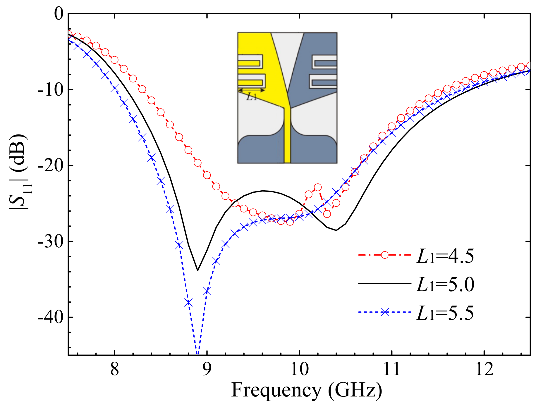
2.2. Structure Parameter Analysis

According to the radiation principle of the tapered slot line antenna, the opening w of the metal patch slot of the antenna determines the bandwidth. In order to obtain preferred antenna performance in the X band, we set the value of w to 5 mm, 6 mm, and 7 mm, and performed a parameter scan simulation, respectively. The reflection coefficient is shown in Figure 4. It is easy to see from the figure that as w increases, the antenna impedance bandwidth is continuously expanded, which has a certain impact on the impedance performance. In order to consider the bandwidth performance and impedance performance, for this design we selected w = 6 mm as the final antenna size parameter.
The U-shaped slot changes the current distribution on the antenna surface to achieve the purpose of miniaturization. To obtain the expected performance results, it is necessary to continuously optimize the size parameters of the U-shaped slot. Here, the value of L1 was set to 4.5 mm, 5 mm, and 5.5 mm. The simulation reflection coefficient is shown in Figure 5. As the value of L1 changes, the resonance frequency of the antenna changes at the low frequency, and the better the impedance performance is responding to the larger L1. Considering all factors, the overall performance of the broadband array was weighed, and finally L1 = 5 mm was selected.
We also checked the other parameters, such as w1, L2, and Ls. However, we found the impact on the |S11| and gain trivial. Although we calculated them by using a generic algorithm to find the requirement of the operating frequency band, both |S11| and gain were scanned as objective functions, as well as input impedance. We also tried other optimization algorithms, such as the grasshopper optimization algorithm [26], firefly algorithm with adaptive cost function [27], and NUFFTs and CUDA [28] methods, etc. To save space, these procedures are not listed in the figures. Finally, the designed parameters of the antenna element are listed in Table 1, which relates to Figure 1.

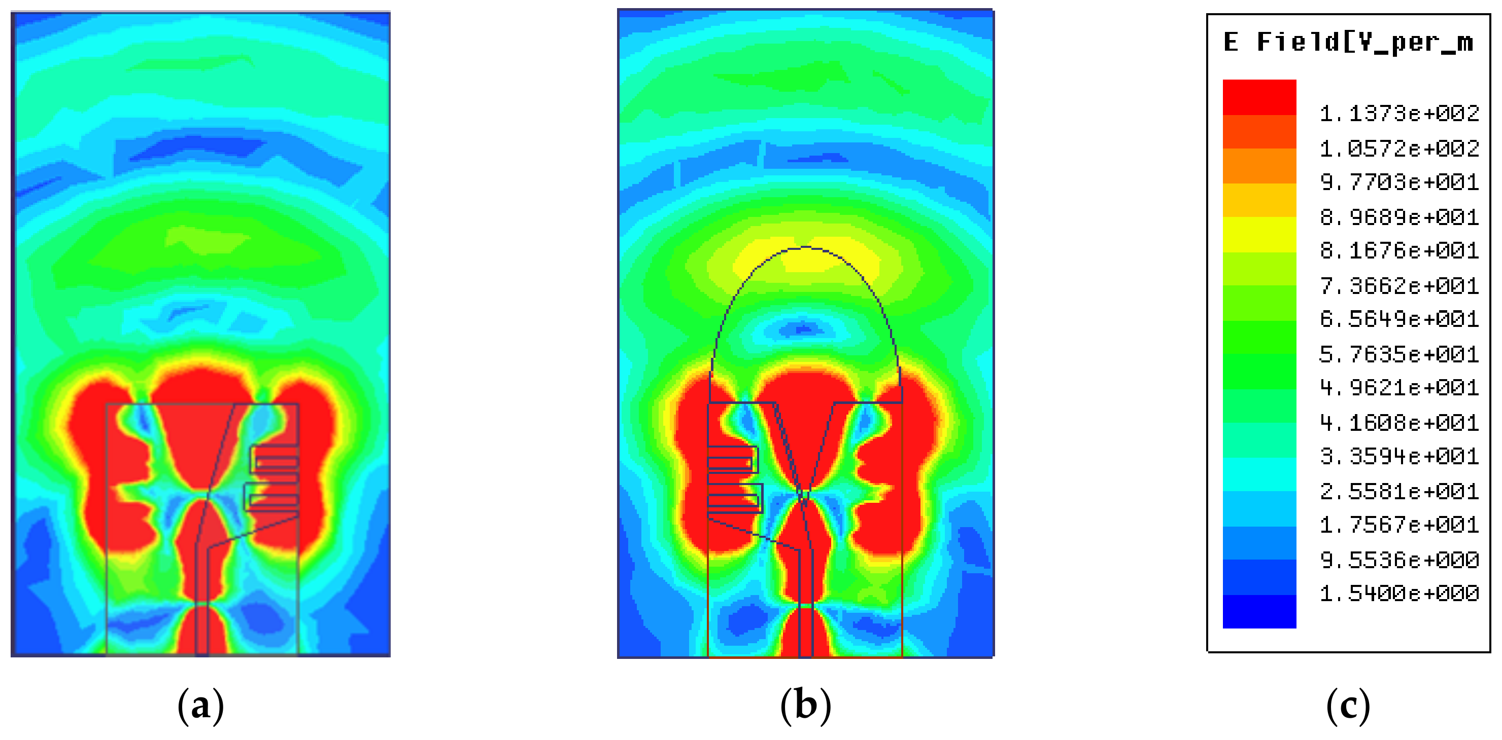
2.3. Field Distribution Analysis

In order to further explain the role of the elliptical dielectric lens, the E-field distribution was simulated, as shown in Figure 6 and Figure 7, where the E-field behaviors are presented. In Figure 6, the frequency of the excitation source at 10 GHz is shown with the E-field distributions for the TSA both with and without dielectric lens loaded. The substrate produced a different propagation environment for the TSA aperture. Employing the dielectric lens, we found the E-field components converged towards the axis of the gap. The directivity of the antenna was enhanced and the gain increased at the same time. When the frequency was increased, such as to 11 GHz of the excitation source, the same results were obtained, as shown in Figure 7. These results tell us the dielectric lens acts as a dielectric wave guide that directs the radiating wave to the aperture center, and strengthens the field coupling in two arms of the TSA, resulting in electromagnetic waves propagating similar to plane-like waves.

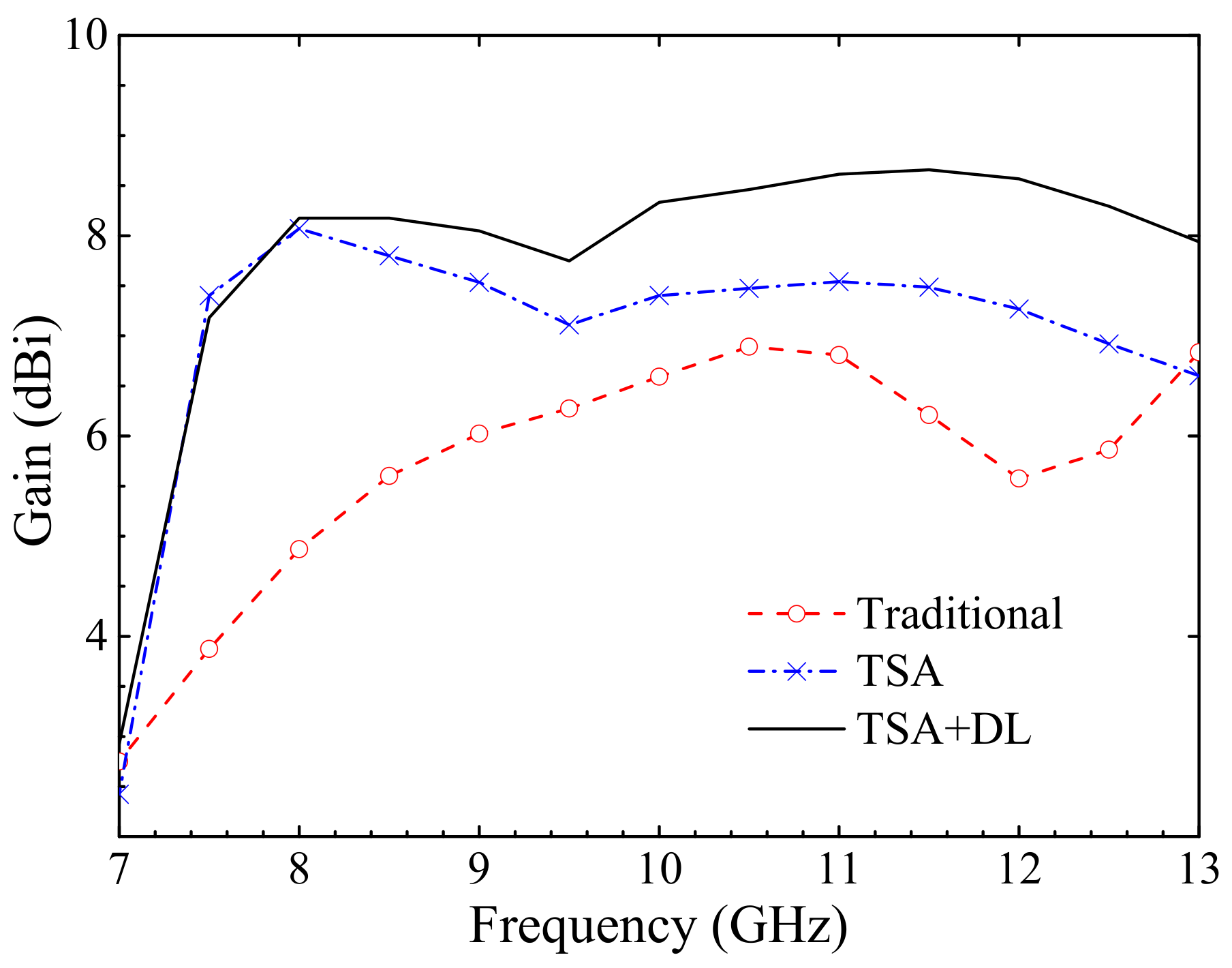
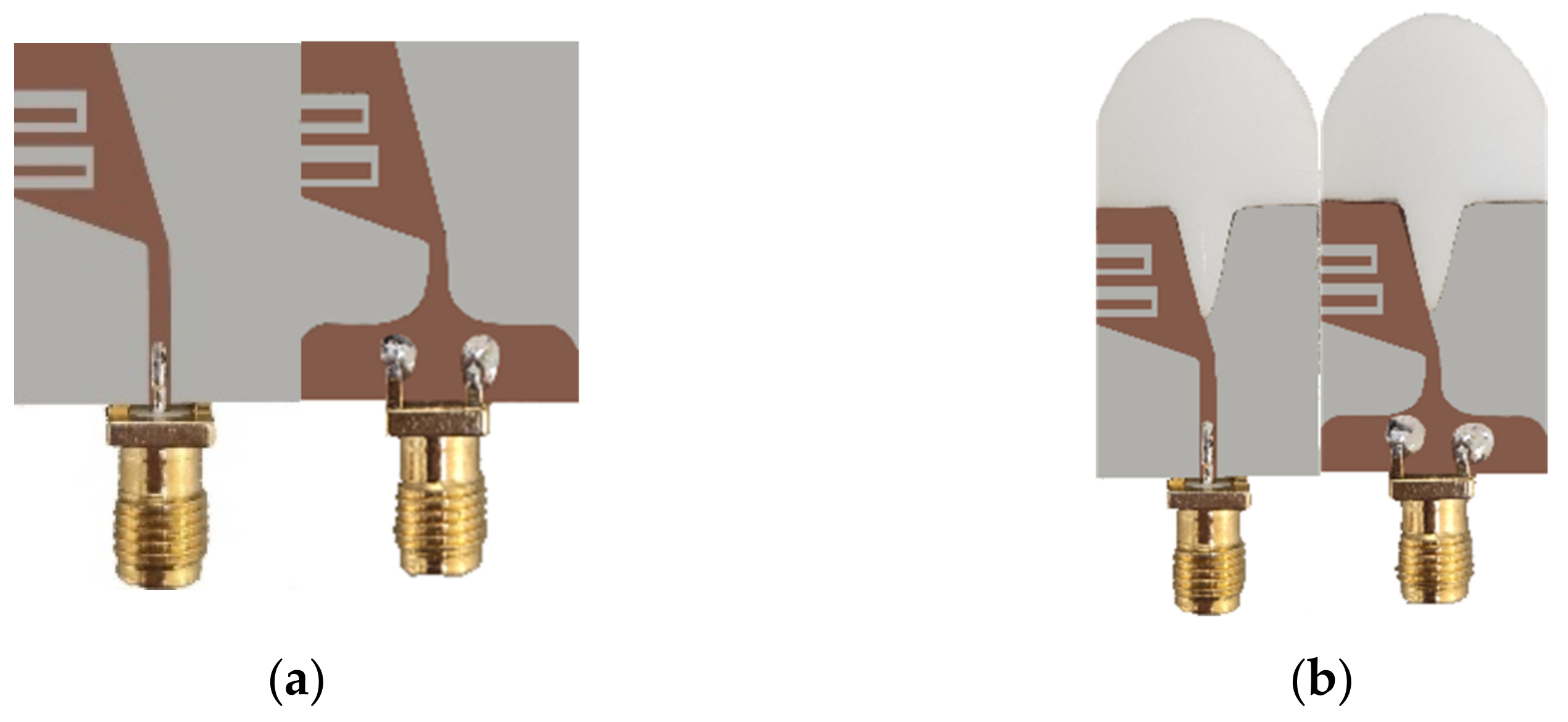
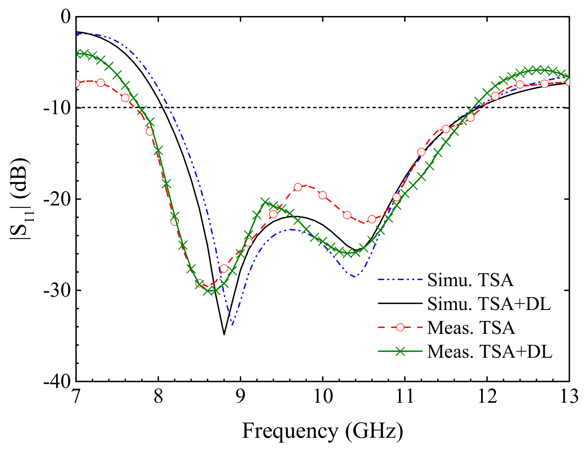
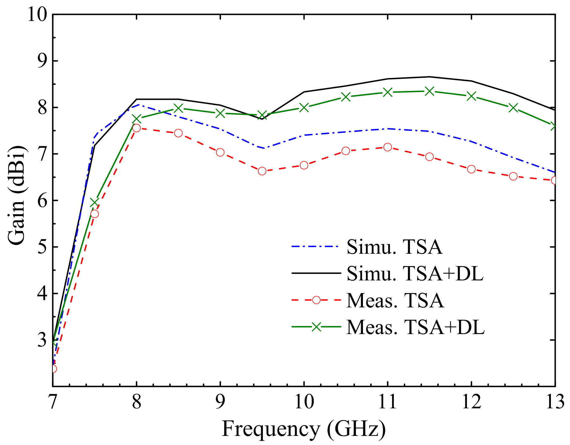
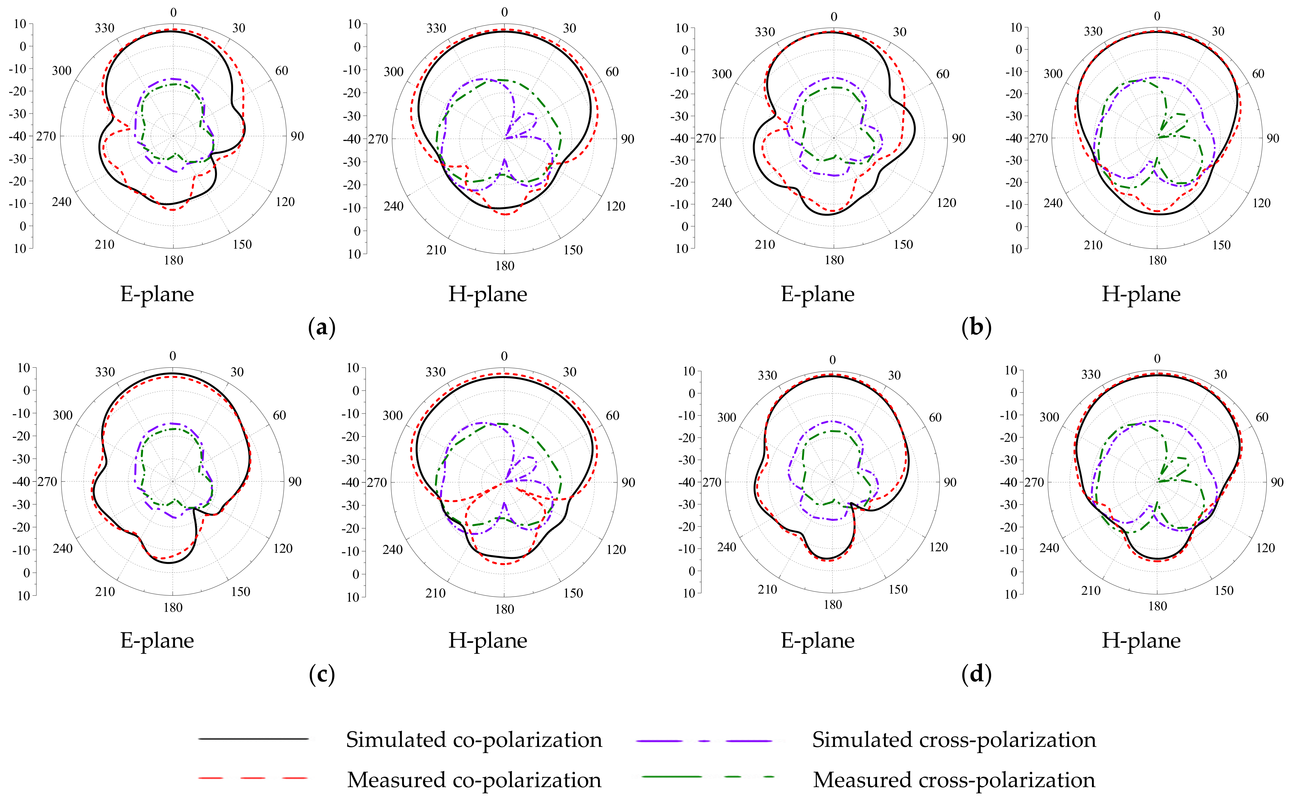
2.4. Results of the Antenna Element Experiment

This design was verified by experiment. A fabricated sample with dimension sizes shown in Table 1 and in Figure 8 was tested in our laboratory. We used the vector network analyzer Keysight N5244A (10 MHz–43.5 GHz). Results of both TSAs demonstrate the specifications of the proposed antenna. DL are generally used to improve different characteristics of a TSA with the same size as that shown in Figure 6b and Figure 7b.
In addition, an elliptical shaped lens can reduce the mismatching between the dielectric and air interface [17]. After checking with simulation software HFSS, we described the antenna size in Table 1. With the dielectric lens, the properties of the antenna were improved significantly. The material of the substrate adapted to the Rogers 3003 with relative dielectric permittivity of εr = 3, a loss tangent of δ = 0.0013, and thickness Eh = 0.762 mm. Different materials in front of the antenna aperture axis had different effects on gain. Thus, the best radiation performance in this approach was implemented by using Teflon material in a dielectric lens with dielectric constants εr = 2.1, which was checked using simulation software.
The measured |S11| and gain of the TSA samples with and without the dielectric lens are depicted in Figure 9 and Figure 10, respectively. It can be seen from the figures that the simulated and measured bandwidth can cover 8.46–11.8 GHz and 7.8–11.9 GHz without the DL, and 8.5–11.8 GHz and 7.85–11.9 GHz with the DL, respectively. As a comparison, simulation results are shown in the same figure, which are in very good agreement with the measurements. Furthermore, the input impedance was still maintained when we loaded the modified elliptical dielectric lens at the antenna aperture axis, because of the advantage of the lens being reflected in the radiation behavior, especially enhancing the gain. From the figure, it is observed that the TSA without the DL presented a gain of 6.61–7.98 dBi and 6.53–7.52 dBi within the operating frequency band. Conversely, the gain of the antenna was significantly improved when loaded with the DL. The maximum gain improvement of 1.62 dBi was obtained at 9.5 GHz. There was a 0.4 dBi error between the simulation and the experiment, but the main reasons were misalignment and fabrication errors.
To further demonstrate the higher gain property with the dielectric lens, the measured radiation patterns of the TSA with and without the dielectric lens are shown in Figure 11 at different frequencies. It was found that the TSA had end-fire radiation directed to the symmetrical axis of the slot aperture. The gain was enhanced and the directivity and half-power beam width significantly improved at 10 GHz and 11 GHz. With the dielectric lens, the antenna gain increased along with the radiation beam becoming stronger and more stable, especially at higher frequencies.
As a comparison, simulated results are also depicted in figures, as well as both co-polarization and cross-polarization. We found that measurement results from the figures were in very good agreement with the simulation.

3. Antenna Array Design

In order to meet practical application requirements, an antenna array was designed which consisted of four elements. The feed network was considered by using a 1–4 Wilkinson power divider. Before designing the feed point of the power splitter, we obtained isolation between the antennas at different ports by feeding the four ports separately. Due to the symmetry of the array of the designed antenna, we only needed to examine the isolation between ports 1 and 2 and ports 2 and 3. Figure 12 shows the simulated port isolation. It can be seen that the isolation of S12 and S23 was both less than −25 dB in the working band of 8–12 GHz, which fully reflects the feasibility of the design.
To reach the goal of higher gain and better directivity, the designed antenna element above with dielectric lens loaded was constituted as a 1 × 4 array, as shown in Figure 13, which was fed by a 1–4 Wilkinson power divider. Each element could be excited with equivalent input magnitude. To maintain good isolation of each output ports, two isolation resistances were used, as shown in Figure 13a; and reasonable elements spacing was followed in the grating lobe analysis [24] to avoid the grating lobe and mutual coupling occurrences of this array. Therefore, the distance between two elements was obeyed by
d a < λ 0 1 + cos ϕ 0
where λ0 and φ0 are the wavelength at the operating frequency and main radiation beam angle, respectively, which is equal to 90 degrees in the E-plane of this proposed array.

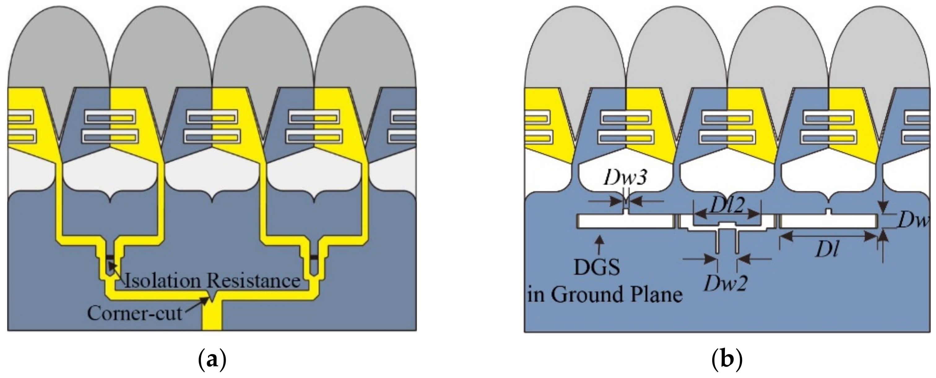
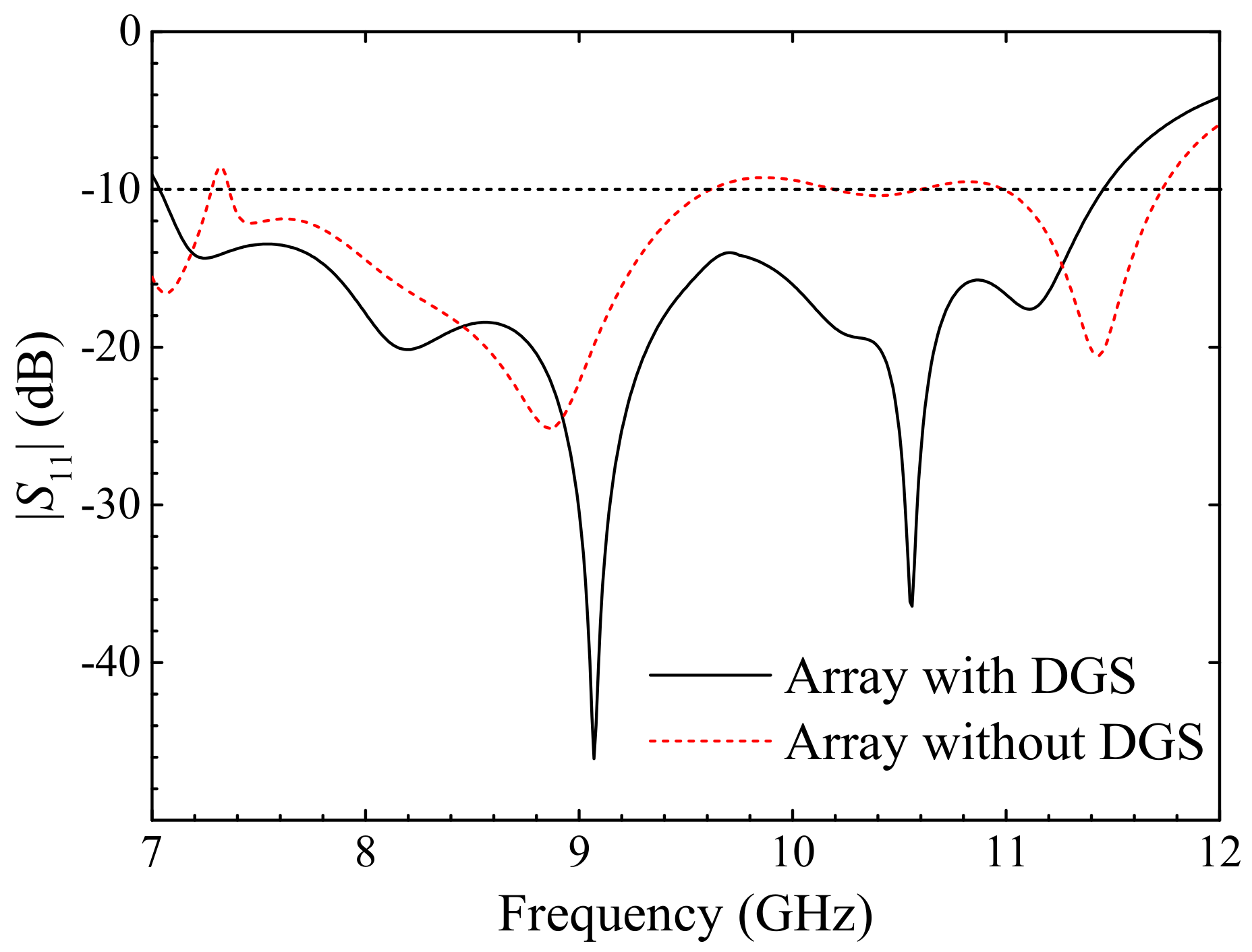
3.1. Defective Ground Structure Design

However, mutual coupling of the adjacent radiation arms of the proposed array could occur due to the four right radiation arms being terminated in the common ground plane, which would worsen the radiation property of the array. To decrease the mutual coupling in antenna elements and improve the input impedance bandwidth, a defective ground structure (DGS) was designed because most of the coupling energy transmits in the form of ground surface waves between antenna elements. A specific irregular rectangular pattern was etched on the metal common ground between adjacent antenna units. The defective structure of the ground plane of the transmission line reconstructs the path distribution of the ground plane surface current. This change will cause the connection impedance characteristic of the ground changes. Through continuous optimization and adjustment, a DGS structure that effectively improved the performance of the array was finally obtained which was embedded in the common ground plane between adjacent arms, as shown in Figure 13b, with dimensions and sizes listed in Table 2. Taking this measure into account, direct near-field mutual coupling will be effectively prevented. Figure 14 displays the impedance bandwidth performance of the proposed array with and without the DGS; it can be easily observed that the proposed array with the DGS has a wide impedance bandwidth and better impedance performance at 7–11.5 GHz.

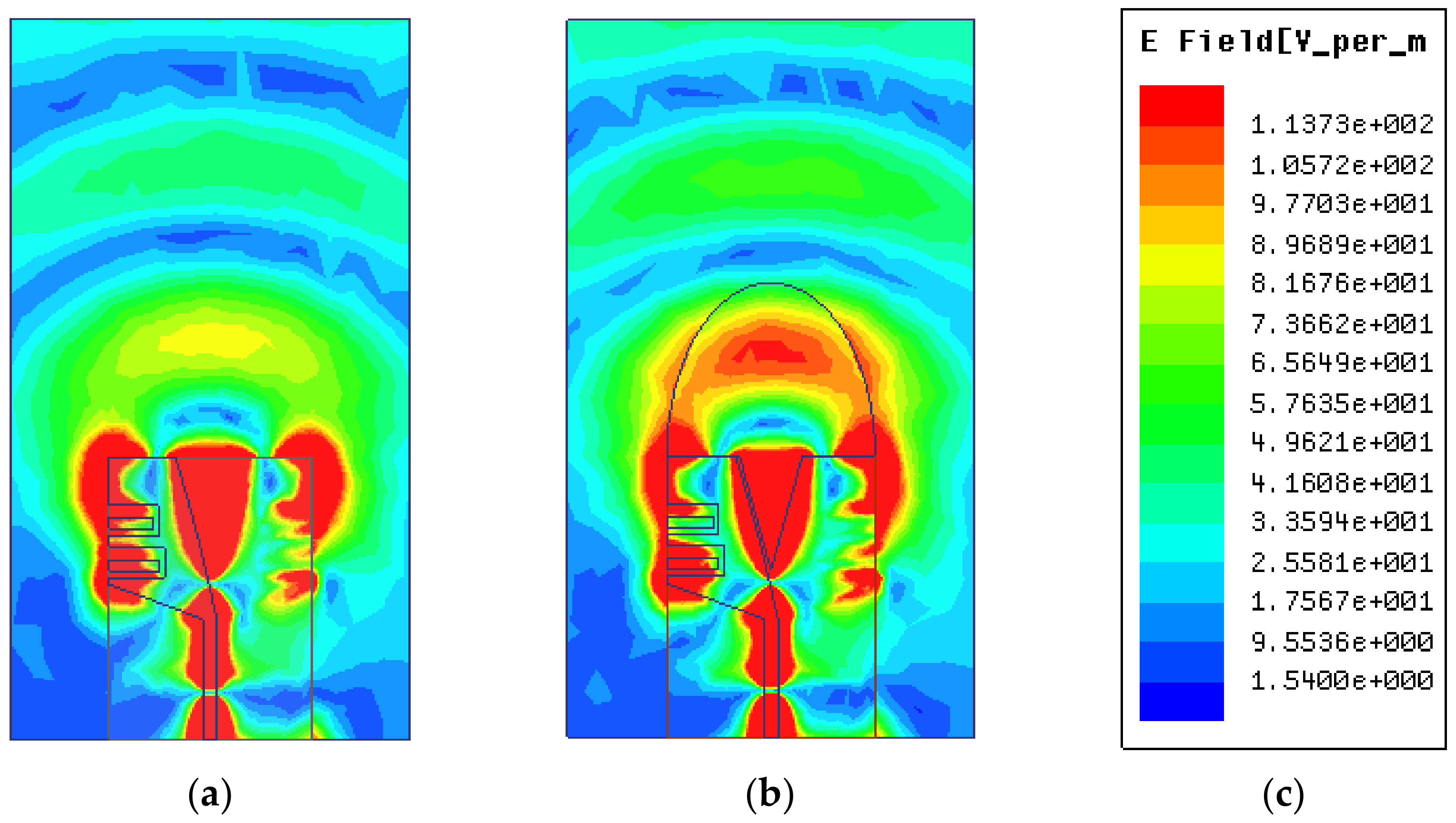
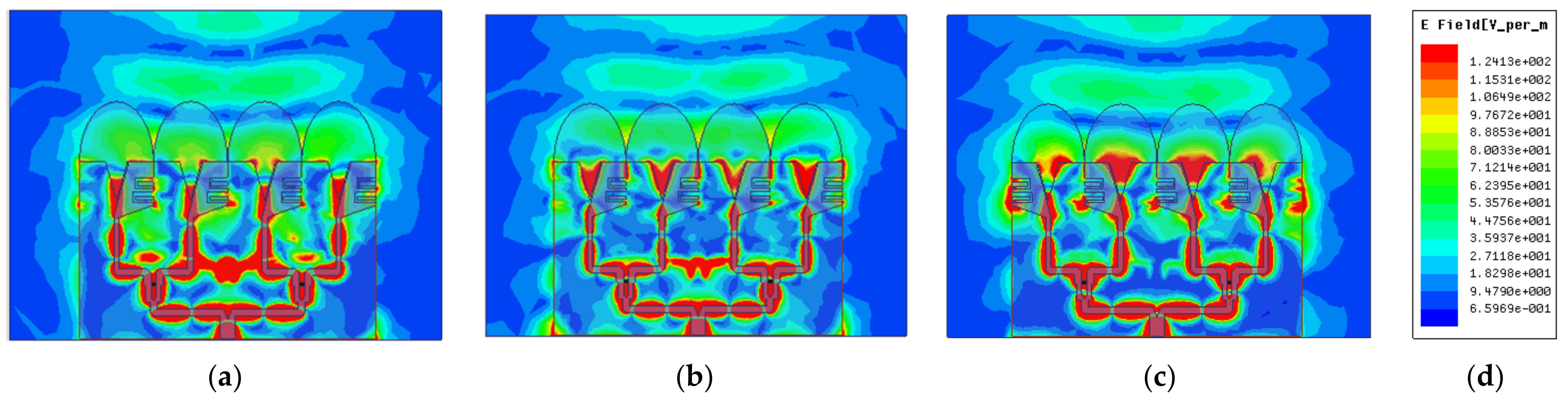
3.2. Field Distribution Analysis

To exhibit the end-fire radiation characteristics further, the E-field distribution of the proposed array at 9 GHz, 10 GHz, and 11 GHz was simulated. Results are depicted in Figure 15. It is obvious that plane waves could be obtained with the dielectric lens and DGS techniques. In addition, it must be noted that with the dielectric lens loaded, the radiation intensity of the array was affected at higher frequency due to strong field coupling to the lenses and the increased radiating energy focused in the end-fire direction. Additionally, the DGS could be used to improve the bandwidth of the array due to current distribution changes.

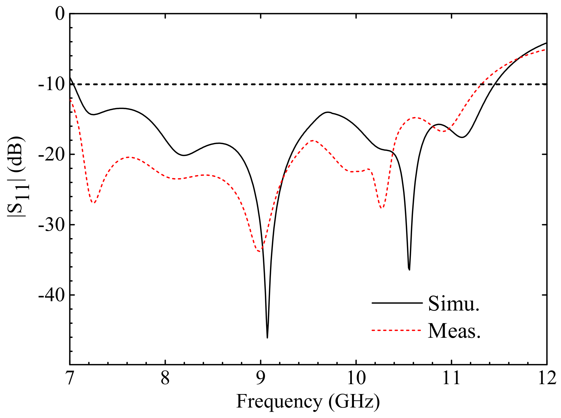
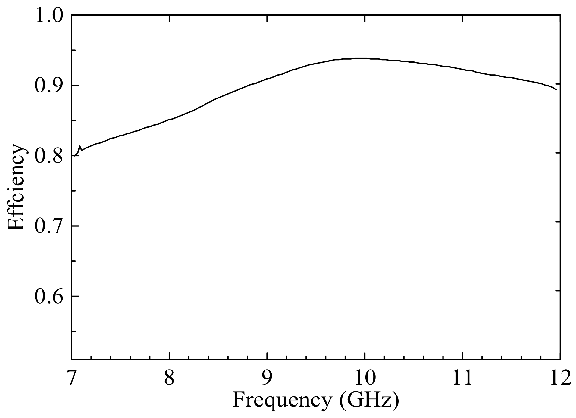
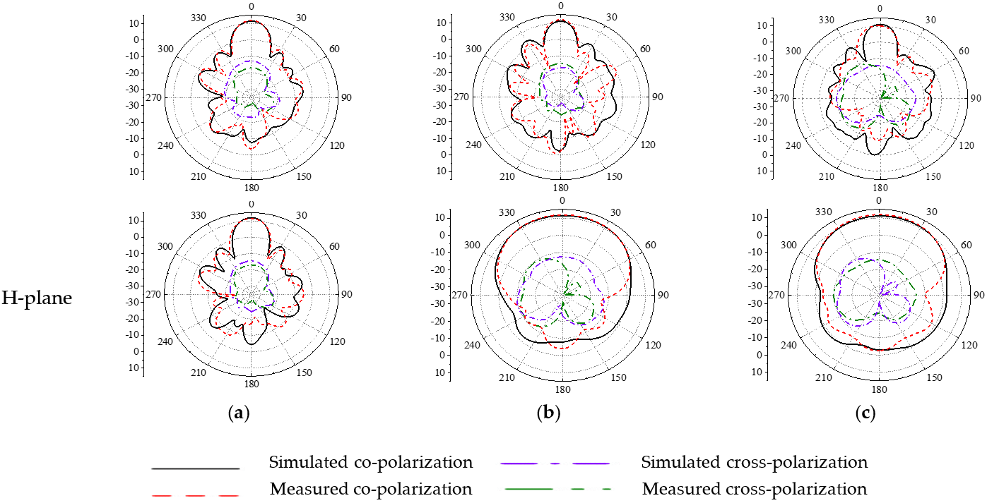
3.3. Measured Results and Discussion

To test the actual working performance of the designed antenna, according to the optimized size parameters of the simulation, the actual antenna and the dielectric lens were processed by the engraving machine. The photographs of the array sample are shown in Figure 16. A series of RF experiments were carried out on the finished antenna using the Agilent vector network analyzer N5244A and a microwave anechoic chamber, including the actual measurement of S parameters, gain, and patterns. The measured site and the |S11| of the antenna arrays are depicted in Figure 17, where the simulated data are reference checked. As can be seen from Figure 18, the |S11| of the proposed array has a DGS less than −10 dB in the frequency bands of 7–11.2 GHz, which still covers X-band communication systems.
On the other hand, the radiation efficiency verses the frequency curve must be considered because this is very important from the point of view of application. A high antenna efficiency, better than 80.0% that of the TSA+DL, was achieved, as shown in Figure 19. In addition, the simulated minimum and maximum efficiency of the ATSA-DL was 80.2% at 7.0 GHz and 93.7% at 10.17 GHz, respectively. We compared the single and array antennas to decide which form of antenna to use (single element or array). Results are listed in the Table 3. We found the performance of the array was much better than the single element antenna in gain, beside the size.
To view the proposed antenna array, the radiation pattern was tested in our laboratory. The testing scenarios in the microwave anechoic chamber and boresight gain are shown in Figure 20 and Figure 21, respectively. From Figure 21, we can see the experiment result was in very good agreement with the simulation.
As observed from Figure 21, the simulated gain increased with the frequency range covering 7–10.7 GHz. In the desired X-band frequency band, the measured minimum gain was at 8 GHz with a 9.1 dBi, and maximum gain was 12.1 dBi at 10.7 GHz. Meanwhile, it should not be neglected that the usage of the microstrip lines will impact the gain of the proposed array at higher frequencies because of the higher insertion loss.
Far-field radiation patterns of the E- and H-planes at frequency points 9 GHz, 10 GHz, and 11 GHz were measured in the same anechoic chamber. Results are shown in Figure 22, where simulated radiation patterns of the E-plane and H-plane are presented in the same figure as comparison. Obviously, the measured results were in good agreement with the simulation. The measured maximum gain at different frequencies in the E-plane and H-plane agree with the simulated results. The proposed array has end-fire characteristics with the more directional main lobe in the axial direction of the tapered slot. Remarkably, the E-plane radiation pattern had an expectable narrow main lobe and low side lobe due to the E-plane arrangement of array elements. Additionally, symmetry of the radiation beam was obtained owing to the symmetrical Wilkinson power divider feed network.
In order to demonstrate the performance improvement of the antenna array, we compared the working band, impedance bandwidth, and gain of the antenna before and after adding the array, as shown in Table 4. It can be seen from the table that when the antenna was assembled, the impedance bandwidth increased by 7.2% without changing the working band, and the gain was greatly increased from 8.43 to 12.4 dBi.
To further illustrate the advantages of the proposed antenna array in radiation performance, we compared its bandwidth and gain with other end-fire antenna arrays. The detailed information is listed in Table 4. It can be seen from [20,21] that the antenna array is fed by the substrate-integrated wave guide (SIW) feed network, with low insertion loss and good broadband performance in the millimeter wave band. Although this feed method can achieve high gains, the relative size is bigger and fabrication complex. Compared to the microstrip line feed array in Table 4, the proposed antenna uses four elements to achieve higher gain. In addition, the relative bandwidth has been greatly improved compared to that in the previous literature. Due to its compact structure and a small number of elements, the overall size of the antenna array is greatly reduced. Therefore, compared with other array antennas, the size advantage of this array antenna is more obvious.

4. Conclusions

In this approach, the performance of a miniaturized antipodal TSA array with gain-enhanced ellipse dielectric lens is reported in detail. Bandwidth from 7–11.2 GHz was achieved. End-fire radiation characteristics were improved with the dielectric lens loaded, which generated near-field plane-like waves across the whole operating frequency, especially at high frequencies. The same plane wave was achieved at different frequencies, which was simulated as shown in Figure 15. Meanwhile, a broadband and compact array with impedance bandwidth of 7–11.2 GHz was presented utilizing the DGS to reduce mutual coupling between array elements and improve the gain of the desired frequency band. The DGS was added on the ground plane and showed good directivity with gain of up to 12.1 dBi. A compact structure makes the proposed array suitable for integration in devices for X-band communication applications. Future research work will focus on circular polarized antenna arrays with wider beam scanning.

Author Contributions

Conceptualization, H.Z. and Y.Z.; methodology, J.W. and W.C.; validation, R.L., M.W. and C.F.; formal analysis, J.W.; investigation, W.C.; writing—original draft preparation, Y.Z.; writing—review and editing, H.Z.; supervision, E.L.; project administration, H.Z. and E.L. All authors have read and agreed to the published version of the manuscript.

Funding

This research was funded by National Natural Science Foundation of China, Grant Number: 62071166, 62071424.

Institutional Review Board Statement

Not applicable.

Informed Consent Statement

Not applicable.

Data Availability Statement

No data.

Conflicts of Interest

The authors declare no conflict of interest.

References

  1. Kharkovsky, S.; Ghasr, M.T.; Abou-Khousa, M.A.; Zoughi, R. K-band varactor diode-tuned elliptical slot antenna for wide-band imaging. IEEE Trans. Antennas Propag. 2011, 59, 4325–4328. [Google Scholar] [CrossRef]
  2. Yngvesson, K.; Korzeniowski, T.; Kim, Y.-S.; Kollberg, E.; Johansson, J. The tapered slot antenna-a new integrated element for millimeter-wave applications. IEEE Trans. Microw. Theory Tech. 1989, 37, 365–374. [Google Scholar] [CrossRef]
  3. Janaswamy, R.; Schaubert, D. Analysis of the tapered slot antenna. IRE Trans. Antennas Propag. 1987, 35, 1058–1065. [Google Scholar] [CrossRef]
  4. Oraizi, H.; Jam, S. Optimum design of tapered slot antenna profile. IEEE Trans. Antennas Propag. 2003, 51, 1987–1995. [Google Scholar] [CrossRef]
  5. Zhang, Y.; Li, E.; Wang, C.; Guo, G. Radiation enhanced Vivaldi antenna with double-antipodal structure. IEEE Antennas Wirel. Propag. Lett. 2016, 16, 561–564. [Google Scholar] [CrossRef]
  6. Malakooti, S.-A.; Moosazadeh, M.; Ranasinghe, D.C.; Fumeaux, C. Antipodal Vivaldi antenna for sum and difference radia-tion patterns with reduced grating lobes. IEEE Antennas Wirel. Propag. 2017, 1, 3139–3142. [Google Scholar] [CrossRef]
  7. De Oliveira, A.M.; Perotoni, M.; Kofuji, S.; Justo, J. A palm tree antipodal Vivaldi antenna with exponential slot edge for improved radiation pattern. IEEE Antennas Wirel. Propag. Lett. 2015, 14, 1334–1337. [Google Scholar] [CrossRef]
  8. Natarajan, R.; George, J.V.; Kanagasabai, M.; Shrivastav, A.K. A compact antipodal Vivaldi antenna for UWB applications. IEEE Antennas Wirel. Propag. Lett. 2015, 14, 1557–1560. [Google Scholar] [CrossRef]
  9. Liu, Y.; Zhou, W.; Yang, S.; Li, W.; Li, P.; Yang, S. A novel miniaturized Vivaldi antenna using tapered slot edge with resonant cavity structure for ultrawideband applications. IEEE Antennas Wirel. Propag. 2016, 15, 1881–1884. [Google Scholar] [CrossRef]
  10. Adam, A.M.; Altalhi, T.A.; El-Megharbel, S.M.; Saad, H.A.; Refat, M.S. Using a modified molyamidoamine fluorescent dendrimer for capturing environment polluting metal ions Zn2+, Cd2+, and Hg2+: Synthesis and characterizations. Crystals 2021, 11, 92. [Google Scholar] [CrossRef]
  11. Yang, G.; Ye, S.; Zhang, F.; Ji, Y.; Zhang, X.; Fang, G. Dual-polarized dual-loop double-slot antipodal tapered slot antenna for ultra-wideband radar applications. Electronics 2021, 10, 1377. [Google Scholar] [CrossRef]
  12. Juan, L.; Guang, F.; Lin, Y.; Demin, Y. A modified balanced antipodal Vivaldi antenna with improved radiation characteristics. Microw. Opt. Technol. 2013, 55, 1321–1325. [Google Scholar] [CrossRef]
  13. Bourqui, J.; Okoniewski, M.; Fear, E. Balanced antipodal Vivaldi antenna with dielectric director for near-field microwave imaging. IEEE Trans. Antennas Propag. 2010, 58, 2318–2326. [Google Scholar] [CrossRef]
  14. Karmakar, A.; Bhattacharjee, A.; Saha, A.; Bhawal, A. Design of a fractal inspired antipodal vivaldi antenna with enhanced radiation characteristics for wideband applications. IET Microw. Antennas Propag. 2019, 13, 892–897. [Google Scholar] [CrossRef]
  15. Amiri, M.; Tofigh, F.; Ghafoorzadeh-Yazdi, A.; Abolhasan, M. Exponential antipodal Vivaldi antenna with exponential die-lectric lens. IEEE Antennas Wirel. Propag. 2017, 1, 1792–1795. [Google Scholar]
  16. Li, X.; Zhou, H.; Gao, Z.; Wang, H.; Lv, G. Metamaterial slabs covered UWB antipodal Vivaldi antenna. IEEE Antennas Wirel. Propag. Lett. 2017, 16, 2943–2946. [Google Scholar] [CrossRef]
  17. Zhu, S.; Liu, H.; Wen, P. A New Method for achieving miniaturization and gain enhancement of Vivaldi antenna array based on anisotropic metasurface. IEEE Trans. Antennas Propag. 2019, 67, 1952–1956. [Google Scholar] [CrossRef]
  18. Ghassemi, N.; Wu, K. Planar High-Gain Dielectric-loaded antipodal linearly tapered slot antenna for E- and W-band gigabyte point-to-point wireless services. IEEE Trans. Antennas Propag. 2013, 61, 1747–1755. [Google Scholar] [CrossRef]
  19. Liu, H.; Yang, W.; Zhang, A.; Zhu, S.; Wang, Z.; Huang, T. A miniaturized gain-enhanced antipodal Vivaldi antenna and its array for 5G communication applications. IEEE Access 2018, 6, 76282–76288. [Google Scholar] [CrossRef]
  20. Liu, P.; Zhu, X.; Jiang, Z.H.; Zhang, Y.; Tang, H.; Hong, W. A compact single-layer Q-band tapered slot antenna array with phase-shifting inductive windows for endfire patterns. IEEE Trans. Antennas Propag. 2018, 67, 169–178. [Google Scholar] [CrossRef]
  21. Kazemi, R.; Fathy, A.E.; Sadeghzadeh, R.A. Dielectric rod antenna array with substrate integrated waveguide planar feed network for wideband applications. IEEE Trans. Antennas Propag. 2012, 60, 1312–1319. [Google Scholar] [CrossRef]
  22. Dang, T.; Zheng, H.; Wang, L.; Cui, W.; Wang, G. Design of ultra-wideband antenna using tapered slot for low-end frequency extension. Int. J. RF Microw. Comput. Aided Eng. 2019, 29, e21553. [Google Scholar] [CrossRef]
  23. Zhu, S.; Liu, H.; Chen, Z.; Wen, P. A compact gain-enhanced Vivaldi antenna array with suppressed mutual coupling for 5G mm wave application. IEEE Antennas Wirel. Propag. Lett. 2018, 17, 776–779. [Google Scholar] [CrossRef]
  24. Cai, X.; Geyi, W.; Sun, H. A printed dipole array with high gain and endfire radiation. IEEE Antennas Wirel. Propag. Lett. 2017, 16, 1512–1515. [Google Scholar] [CrossRef]
  25. Liang, Z.; Lv, S.; Li, Y.; Liu, J.; Long, Y. Compact folded slot antenna and its endfire arrays with high gain and vertical po-larization. IEEE Antennas Wirel. Propag. Lett. 2020, 19, 789–790. [Google Scholar] [CrossRef]
  26. Mirjalili, S.Z.; Mirjalili, S.; Saremi, S.; Faris, H.; Aljarah, I. Grasshopper optimization algorithm for multi-objective optimization problems. Appl. Intell. 2018, 48, 805–820. [Google Scholar] [CrossRef]
  27. Baumgartner, P.; Bauernfeind, T.; Biro, O.; Hackl, A.; Magele, C.; Renhart, W.; Torchio, R. Multi-objective optimization of Yagi–Uda antenna applying enhanced firefly algorithm with adaptive cost function. IEEE Trans. Magn. 2017, 54, 1–4. [Google Scholar] [CrossRef]
  28. Capozzoli, A.; Curcio, C.; Liseno, A. Fast, phase-only synthesis of aperiodic reflect arrays using NUFFTs and CUDA. Prog. Electromag. Res. 2016, 156, 83–103. [Google Scholar] [CrossRef] [Green Version]
Figure 1. Evolution process of a dielectric lens director introduced into the antipodal TSA: (a) traditional antipodal TSA front and back views of the structure in yellow and blue, respectively; (b) two tapered U-typed slots were introduced, and (c) a dielectric lens director, called a TSA-DL.
Electronics 10 02066 g001
Figure 2. Simulated reflection coefficient of the different structures of the tapered slot antenna.
Electronics 10 02066 g002
Figure 3. The gain of different structures of tapered slot antennas.
Electronics 10 02066 g003
Figure 4. |S11| of the designed antenna with different w (unit: mm).
Electronics 10 02066 g004
Figure 5. |S11| of the designed antenna with different L1 values (unit: mm).
Electronics 10 02066 g005
Figure 6. E-field distribution inside substrate of the TSA element at 10 GHz, (a) without dielectric lens, (b) with dielectric lens, and (c) relative value of electric field strength. The focus of the E-field obviously occurs on the axis of symmetry.
Electronics 10 02066 g006
Figure 7. E-field distribution inside substrate of the TSA element at 11 GHz, (a) without dielectric lens, (b) with dielectric lens loaded, and (c) relative value of electric field strength. The same summary is obtained in Figure 2 and Figure 3.
Electronics 10 02066 g007
Figure 8. Photographs of fabricated single antenna element, (a) TSA and (b) TSA+DL. Both sides of each antenna sample are shown in the figure, and the same form is used in Figure 6b and Figure 7b.
Electronics 10 02066 g008
Figure 9. Measured and simulated |S11| of the designed antipodal tapered slot antenna (TSA), and comparison of two different antenna structures with and without dielectric lens (DL) loaded.
Electronics 10 02066 g009
Figure 10. Measured and simulated gain of the designed antipodal tapered slot antenna (TSA), and comparison of two different antenna structures with and without DL.
Electronics 10 02066 g010
Figure 11. Measured and simulated radiation patterns of the TSA with and without dielectric lens (DL) on the E-plane (left side) and H-plane (right side), (a) without DL and (b) with DL at 10 GHz; and (c) without DL and (d) with DL at 11 GHz.
Electronics 10 02066 g011
Figure 12. Simulated S-parameter of antenna with separate four-port feed.
Electronics 10 02066 g012
Figure 13. Configurations of the proposed antenna array fed by 1–4 Wilkinson power divider with two isolation resistances, (a) front of view and (b) back of view, of the DGS designed on the ground.
Electronics 10 02066 g013
Figure 14. Simulated |S11| of the designed antenna array with and without defected ground structure (DGS). Operating bandwidth of the array improved significantly with the DGS.
Electronics 10 02066 g014
Figure 15. E-field distribution of the proposed array with DGS at (a) 9 GHz, (b) 10 GHz, and (c) 11 GHz and (d) relative value of electric field strength.
Electronics 10 02066 g015
Figure 16. Photograph of the fabricated antenna array with DGS, (a) front view and (b) back view.
Electronics 10 02066 g016
Figure 17. A photograph of the measured |S11| scenarios using vector network analyzer Keysight N5244A.
Electronics 10 02066 g017
Figure 18. Measured and simulated |S11| of the proposed array with DGS, and frequency bands covering 7–11.2 GHz.
Electronics 10 02066 g018
Figure 19. The efficiency of the proposed antenna array was better than 80.0% that of the TSA + DL.
Electronics 10 02066 g019
Figure 20. Measurement of the proposed antenna array scenario in the microwave anechoic chamber.
Electronics 10 02066 g020
Figure 21. Measured and simulated gain of the proposed array at 7–12 GHz.
Electronics 10 02066 g021
Figure 22. Measured and simulated radiation patterns of the proposed antenna array in the E-plane (top line) and H-plane (bottom) at (a) 9 GHz, (b) 10 GHz, and (c) 11 GHz.
Electronics 10 02066 g022
Table 1. Dimensions and size of antenna elements (unit: mm).
ParameterLWwWfYfL1
Size23.51861.2145
ParameterL2W1LsEwElEh
Size4.52.510.518173
Table 2. Dimensions and size of the DGS as shown in Figure 13b.
ParameterDlDwDl2Dw2Dw3
Size17.421233
Table 3. Comparison of the performance of the antenna element and array.
TypeFrequency (GHz)Bandwidth (%)Gain (dBi)
SimulatedMeasured
Single antenna7.8–11.941.68.438.35
Antenna array7–11.548.612.412.1
Table 4. Comparison of results from some previous antenna arrays in the literature.
Ref.Performance Parameter Feed TypeNumber of ElementsBandwidth (GHz)Size
λ × λ × λ
Gain
(dBi)
[17]Microstrip Line824.6–28.5 (14.69%)6.22 × 2.99 × 0.0811.3
[18]SIW470–103 (38.15%)9.4 × 3.5 × 0.1219.1
[19]Microstrip Line824.75–27.5 (10.53%)4.71 × 7.45 × 0.0412.9
[20]SIW438.9–44.5 (13.42%)4.56 × 4.52 × 0.03614.9
[21]SIW88–12 (25%)4 × 3.6 × 0.3216.5
[23]Microstrip Line824.8–28.5 (13.88%)6.22 × 2.99 × 0.0811.2
[24]Microstrip Line42.26–2.54 (5.83%)1.44 × 0.48 × 0.09610
[25]Microstrip Line85.22–5.64 (7.73%)1.8 × 1.4 × 0.082313.2
This workMicrostrip Line47–11.2 (46.15%)1.43 × 2.40 × 0.0312.1
Publisher’s Note: MDPI stays neutral with regard to jurisdictional claims in published maps and institutional affiliations.

