1. Introduction
In recent years, the rapid development of WLANs has played an increasingly important role in communication systems. The PLL is one of the most critical building blocks in wireless transceivers [
1,
2,
3,
4]. The constantly updated WLAN technology introduces higher requirements on frequency synthesizers. A PLL that multiplies low-frequency reference clocks to generate high-frequency clocks is usually designed with a ring voltage-controlled oscillator (ring-VCO) or an LC VCO. However, an LC VCO shows high sensitivity to magnetic coupling and occupies a large silicon area. Hence, the ring-VCO-based PLL is preferable in many applications. Its main advantages are a very small die area, which reduces the integrated circuit (IC) cost and helps minimize the substrate noise and spur coupling, and a wide tuning range.
PLL is a closed-loop feedback system [
5,
6,
7]. The loop bandwidth and damping factor of the PLL will affect the PLL loop characteristics, such as the stability and locking time [
8,
9,
10]. Usually, the PLL output frequency is variable, and there is an output range, especially for wideband PLL. We usually adjust the PLL output frequency by changing the reference frequency and the division ratio of the divider. However, the loop bandwidth of the traditional PLL cannot track the reference input frequency and the loop frequency division ratio, resulting in a narrow operating frequency range. Moreover, the loop bandwidth is set to be small for stability, resulting in a long locking time and poor jitter performance. The loop damping factor is affected by the frequency division ratio and the process, voltage, temperature (PVT). It is not a fixed value, which leads to the deterioration of the stability of the PLL. The problems mentioned above pose a higher challenge for the design of high-performance PLLs.
The PLL based on self-biased techniques is attractive for solving these problems [
11,
12,
13,
14,
15]. The self-biased PLL has the following advantages:
It is completely self-biased and does not require additional voltage and current bias circuits, so it has a smaller area.
The loop bandwidth follows the input reference frequency. The loop bandwidth can be set to be relatively large, so that the lock time of the PLL is relatively short, and the anti-jitter ability is relatively strong.
The self-biased phase-locked loop has a fixed damping factor, and the stability of the loop is not affected by the input reference frequency, frequency division ratio, etc., so the stability of the self-biased phase-locked loop is very good.
The damping factor and the ratio of loop bandwidth to input reference frequency are completely determined by the ratio of capacitance and have nothing to do with the PVT and other factors.
The self-biased PLL can automatically adjust the operating point of the bias circuit to the optimum according to the working environment (the oscillation frequency of the VCO), thereby achieving self-adaptation.
The self-biased PLL can adapt to different input reference frequencies and frequency division ratios, and can adapt well to different application requirements.
However, many self-biased PLLs [
11,
12,
13] whose loop bandwidth cannot track the division ratio have removed the division ratio effect, and the bandwidth is unchanged when the reference clock is stable. The low-pass filter (LPF) is a key module in PLL. It converts the charge/discharge current of the charge-pump (CP) into VCO tuning voltage, filters the ripple on VCO tuning voltage, reduces the fluctuation of VCO tuning voltage, and improves the jitter performance of PLL. Although PLLs use self-biased technology in reference [
11,
12], all those mentioned above use first-order LPF. The first-order LPF cannot effectively filter the ripple of VCO tuning voltage and also makes PLL unable to achieve low phase noise and jitter performance. Therefore, second-order or third-order LPF is required to obtain low jitter PLL. The bias generation circuits in [
13] occupy a large area. Although a self-biased PLL without any bias circuit [
14] was proposed, the operational amplifier (OPA) in the voltage-to-current (VI) converter consumes considerable power, especially when the loop bandwidth is large. Moreover, because the charge/discharge current of the self-biased PLL is a monotonically increasing function of the VCO frequency, it is extremely low when the VCO begins oscillating after a power-up. Therefore, the classical self-biased PLL always exhibits a very long power-up latency to approach locking at a required frequency. To speed up the locking process of the PLL, an initialization circuit is added to the PLL [
15]. The function of this initialization circuit is to set the current of the charge-pump to the maximum value and discharge the tuning voltage of the VCO close to the ground level when the PLL is powered on. At this time, the VCO oscillates at the highest frequency. If the target frequency is high, the locking time of the PLL will be reduced. However, if the target frequency is low, the locking time will still be very long.
Based on the problem mentioned above, this paper presents a novel self-biased PLL scheme. The main contributions of this paper are listed below:
The novel self-biased scheme is very simple to implement and has the characteristics of small area and low power consumption.
Regardless of whether the target frequency is high or low, the proposed start-up circuit is very effective and can accelerate the locking of the PLL.
A differential-to-single-ended (DTS) converter is presented to reduce the operating frequency and obtain a single-ended output with a 50% duty cycle.
In this paper, a novel self-biased circuit that contains a current mirror circuit and a variable resistor circuit related to the frequency division ratio is proposed. The variable resistor is used in the LPF. The second-order LPF is used in the proposed PLL, which is a third-order PLL, to obtain better phase noise and jitter performance. Moreover, the bias current of the charge-pump and VCO is provided by the self-biased circuit, which limits power consumption and area. With the self-biased circuit, both the current of the VCO delay cells and the charge/discharge (ICP) current of the charge-pump change with the VCO tuning voltage of (VCTRL) by quadratic functions. Therefore, a start-up circuit is needed to speed up the PLL locking. The proposed start-up circuit can increase the VCO tuning voltage to 600 mV in a very short time. Moreover, when the VCO tuning voltage is pulled to 600 mV, the start-up circuit is automatically closed without affecting the normal operation and locking of the PLL. In addition, a DTS converter is presented to reduce the operating frequency and obtain a single-ended output with a 50% duty cycle.
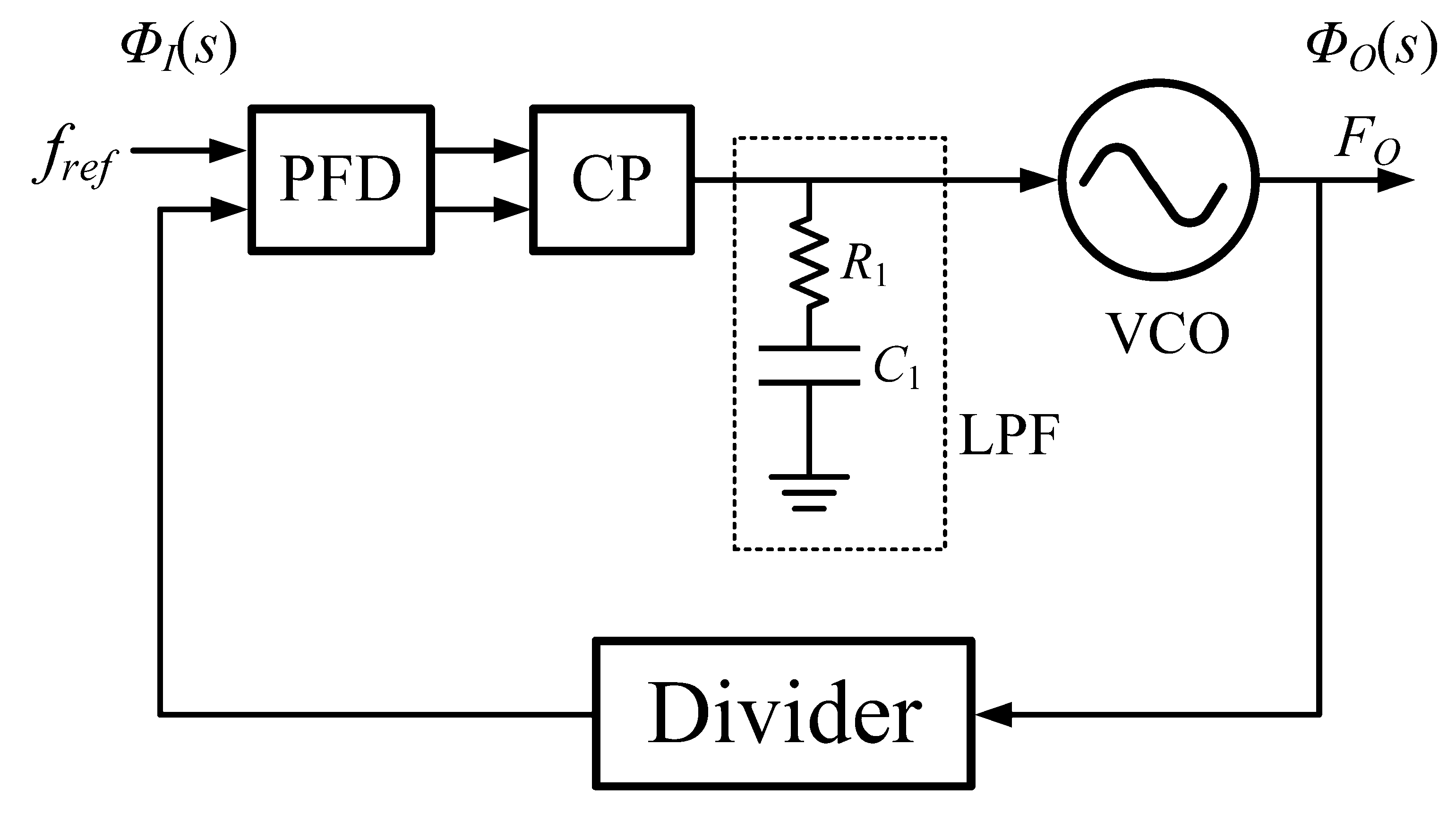
2. The Traditional PLL
A traditional PLL is shown in
Figure 1. It consists of a phase/frequency detector (PFD), a charge-pump, an LPF, a VCO, and a divide-by-N frequency divider. When PLL is locked, there is no phase error between the reference clock and the divider output clock for the charge-pump PLL.
The closed-loop response of the traditional PLL can be easily obtained as Equation (1).
where
ΦI(
s) is the input phase,
ΦO(
s) is the output phase,
R1 is the loop filter resistor,
C1 is the loop filter capacitance,
ICP is the charge pump current,
N is the divider division ratio, and
KVCO is the VCO gain.
We prefer, from control theory, to express the denominator in the form
s2 + 2
ζωns +
ωn2. Thus,
The expressions of the damping factor
ζ and the loop bandwidth
ωn are as follows:
The loop bandwidth and damping factor describe the closed-loop response characteristics of PLL and are important system parameters to be considered when designing PLL. The damping factor ζ has an important influence on the dynamic performance of the PLL. For a critically-damped response, ζ=, we typically choose ζ in the range of and 1. The loop bandwidth ωn must be a decade below the reference frequency for stability. In addition, ωn should be positioned as close as possible to ωref to minimize the total phase error. For a typical PLL, the charge-pump current ICP, VCO gain KVCO, loop filter capacitance C1, and loop filter resistance R1 are changed because of variations in the PVT. Moreover, the division ratio N varies with the PLL output frequency. Therefore, ζ and ωn are changed because of the variation in these parameters. Thus, the loop characteristics of PLL are changeable.
3. The Proposed Self-Biased PLL
In a typical PLL,
ωn and
ζ vary with division ratio
N and PVT. In this paper, we propose a novel self-biased PLL scheme to solve the above problems. The proposed self-biased PLL shown in
Figure 2 is a part of the Wi-Fi chip we designed, and this Wi-Fi chip supports the 802.11ac protocol. The self-biased circuit provides bias voltage and current for the charge-pump, VCO, and LPF. The resistor in LPF is a variable resistor. The VCO is followed by the DTS converter. The start-up circuit is designed to speed up PLL locking by giving the VCO tuning voltage (
Vctrl) an initial value when the PLL starts to work. The PLL has four outputs, among which
FVCO is directly generated by VCO. The VCO is followed by three dividers, which generate
FO1,
FO2, and
FO3. The operating frequency of the VCO in the proposed PLL is 960 MHz. The oscillating signal of the VCO passes through two frequency dividers with a frequency division ratio of 6 to generate two clock signals with a frequency of 160 MHz for the analog-to-digital converter (ADC) and baseband, and a frequency divider with a frequency division ratio of 80 to produce a clock signal with a frequency of 12 MHz for the universal serial bus (USB).
3.1. The Self-Biased Circuit
The proposed self-biased circuit is shown in
Figure 3.
N[0],
N[1],
N[2],
N[3],
N[4],
N[5],
N[6], and
N[7] are the corresponding bits of the 8-bit programmable frequency divider.
The current
I1 is related to
I0 by
where
NT is the OR logic of the 5th, 6th, and 7th bits of the divider. That is,
NT is given by
NTB is the inverse of the NT.
The current
ICP is related to
I0 by
The current
I2 is related to
I1 by
where
N is the division ratio of the divider.
The current
I3 is related to
I2 by
The current
I3 is related to
I1 by
The current
I3 is related to
I0 by
where
Y is given by
3.2. The LPF with a Variable Resistor
The proposed variable resistor is shown in
Figure 4. The variable resistor is composed of three branches. N7B is the inverse of the
N[7]. The transistor size ratio of each branch is 1:6:2.
βP,
βP =
μP·
Cox·
W/
L, represents the transistor parameters of the smallest size branch, and
X represents the relationship between the total size of the transistor of the variable resistor and the smallest size branch.
The product of
X and
Y is given by
Then, the resistance of the variable resistor is given by
3.3. The Proposed Ring-VCO
The requirements of ADC, baseband, and USB for clock jitter performance are not very high. For example, the ADC that we designed requires that the clock jitter is less than 5 Ps. Therefore, considering the phase noise, jitter performance, complexity, area, power consumption, and other factors, we chose the ring oscillator. A ring-VCO consists of many gain stages in a loop. The total number of inversions in the loop must be odd so that the circuit does not latch up. In contrast, the differential implementation can utilize an even number of stages by simply configuring one stage such that it does not invert [
16,
17]. This flexibility demonstrates another advantage of differential circuits over their single-ended counterparts. The number of stages in a ring-VCO is determined by various requirements, including speed, power dissipation, and noise immunity. In most applications, three to five stages provide optimum performance (for differential implementations).
The top architecture of the proposed ring-VCO with three-stage delay cells is illustrated in
Figure 5a. Since each delay cell contributes noise, the three-stage structure can achieve lower phase noise as compared to four- or more-stage designs. The ring-VCO delay cells are the differential buffer delay stages with symmetric loads.
Figure 5b presents the buffer stage which includes a source coupled pair with resistive load elements, called symmetric loads [
9]. Because the effective resistance of the load elements changes with
VBN, the buffer delay also changes with
VBN. In addition, the cross-coupled transistors M1 and M2 in
Figure 5b increase the charge and discharge current of the delay cell, which improves the flip speed of the output level.
The three-stage VCO oscillation frequency is:
where
CT is the total VCO capacitance,
k =
μn·
Cox·
W/
L, and
ID is the drain current for one of the diode-connected NMOS devices biased at VBN. Thus, the VCO gain
KVCO is as follows:
Then, the damping factor
ζ is given by
The loop bandwidth
ωn to operating frequency ratio is:
Equations (18) and (19) show that the damping ζ and the loop bandwidth ωn to operating frequency ratio are constant, and are determined by the capacitance ratio. Equation (19) shows that, with a given N, the bandwidth is proportional to the input reference clock. When N is increased, the bandwidth increases to suppress more VCO noise to achieve better jitter performance. This means that the PLL will be more robust and stable.
3.4. Start-Up Circuit
Self-biased topology avoids the necessity of external biasing. However, the nonlinear capture behavior of a self-biased PLL results in very long power-up latency, which is unacceptable for most applications. With the bias generator, both the VCO delay cells currents and the charge-pump discharge/charge (
ICP) currents change with
VCTRL by quadratic functions [
18,
19]. Therefore, a start-up circuit is needed to speed up PLL locking.
The proposed start-up circuit is shown in
Figure 6. When the PLL is powered on, SWB and PR are low. TE is also low. Transistor M3 mirrors the current to transistor M4, and transistor M2 mirrors the current to transistor M5. SWB turns on transistor M6, charging
VC1 to 600 mV. When the voltage of
VC1 is 600 mV, the transistor M10 is turned on, then the SWB becomes high, and transistor M6 is turned off. At this time, the start-up circuit is closed and the PLL starts to work normally. The SWB and
VC1 levels with time are shown in
Figure 7.
Figure 7 shows that the
VC1 level is pulled up to 600 mV at approximately 4.3 μs, and the SWB level changes from low to high. The SWB level changes from low to high, which turns off transistor M6, and the start-up circuit no longer works. The PLL lock signal is presented in
Figure 8.
Figure 8 shows that the lock signal becomes high at approximately 27 μs, which indicates that the proposed PLL has been locked. The lock time fully meets the usage requirements.
3.5. Differential-to-Single-Ended Converter
Generally, the PLL output should be 50% duty cycle [
20,
21]. We usually use a divider which is divided by 2 to get a 50% duty cycle.
Figure 9 shows the proposed DTS converter scheme. The circuit can generate the needed output clock with a 50% duty cycle. It is made up of two PMOS differential amplifiers driving two CMOS inverters and connected by the cross-coupled transistors M1 and M2 that increase the flip speed of the output level. The two PMOS differential amplifiers use the same current source bias voltage,
VBP, as the VCO delay cells. The role of the two PMOS differential amplifiers is to provide signal amplification. The CMOS inverters provide additional signal amplification and conversion to a single-ended output whose range extends from rail to rail. However, if we use a divider to generate a 50% duty cycle output, the VCOs are designed to operate at twice the chip operating frequency. When the output signal frequency is high with a 50% duty cycle, the designed VCO works at a higher frequency. Therefore, to generate a 50% duty cycle output, this circuit’s design constraints can be relaxed [
9].
Figure 10 illustrates the waveform of the input and output clock of the DTS converter.
Figure 10a shows the output clock of the ring-VCO, which is the input clock of the DTS converter. As shown in
Figure 10a, because of the voltage limitation, the ring-VCO amplitude is not so large that it may not be used directly in digital circuits. Moreover, when the working frequency of the ring-VCO is low, the ring-VCO amplitude will be close to the threshold voltage. The output clock of the DTS converter is shown in
Figure 10b, and its output range extends from rail to rail. In addition, the duty cycle of the output clock is 50%. In this case, the output clock can be directly used in digital circuits.
4. Measurement Results
A micrograph of the proposed PLL fabricated using the SMIC 55 nm CMOS process is shown in
Figure 11, and the chip occupies 253 μm × 349 μm, excluding the I/O pads. The PLL utilizes a reference clock of 40 MHz, which is a crystal oscillator that occupies 290 μm × 136 μm and is integrated into the PLL chip. The proposed crystal oscillator scheme is shown in
Figure 12. It is a parallel crystal oscillator based on the Colpitts structure. The crystal oscillator in the chip photo, which includes resistors, capacitor arrays, inverters, and buffers, is the rest of the circuit except the crystal (the dashed box in
Figure 12). The crystal is soldered on the printed circuit board (PCB) and directly connected to the chip. The chip measurement setup is shown in
Figure 13. The output level of the lock detector is shown in
Figure 14.
Figure 14a shows the output level of the lock detector when the PLL is not locked.
Figure 14b shows the output level of the lock detector when the PLL is locked. As shown in
Figure 14b, the proposed PLL can be locked normally. When the output frequency of VCO is 960 MHz, the output clock frequency of the VCO signal passing through the three-way frequency divider is 160 MHz, 160 MHz, and 12 MHz.
Figure 15 shows the waveform and spectrum of 160 MHz output.
A Rohde & Schwarz FSW50 signal and spectrum analyzer was used to test the phase noise of the PLL.
Figure 16 shows the phase noise of the proposed PLL at a carrier frequency of 960 MHz. The phase noise of the designed PLL is –104.8 dBc/Hz at a 1 MHz frequency offset. The RMS jitter integrated from 10 kHz to 10 MHz is 2.4 ps. There is a spike shown in
Figure 16 at a frequency offset of 40 MHz. The spike, called the reference spur in the spectrum, comes from a reference clock with a frequency of 40 MHz generated by the crystal oscillator. The reference spur is caused by the mismatch of the charge and discharge currents of the charge-pump, which will generate periodic ripples on the tuning voltage of the VCO. A summary of the measured results and performance comparison is given in
Table 1.
Table 1 shows that the figure-of-merit (FoM) is also better than most of the works listed in
Table 1.


