
Multiphysics Analysis and Optimal Design of Compressible Micro-Interconnect for 2.5D/3D Heterogeneous Integration


Abstract
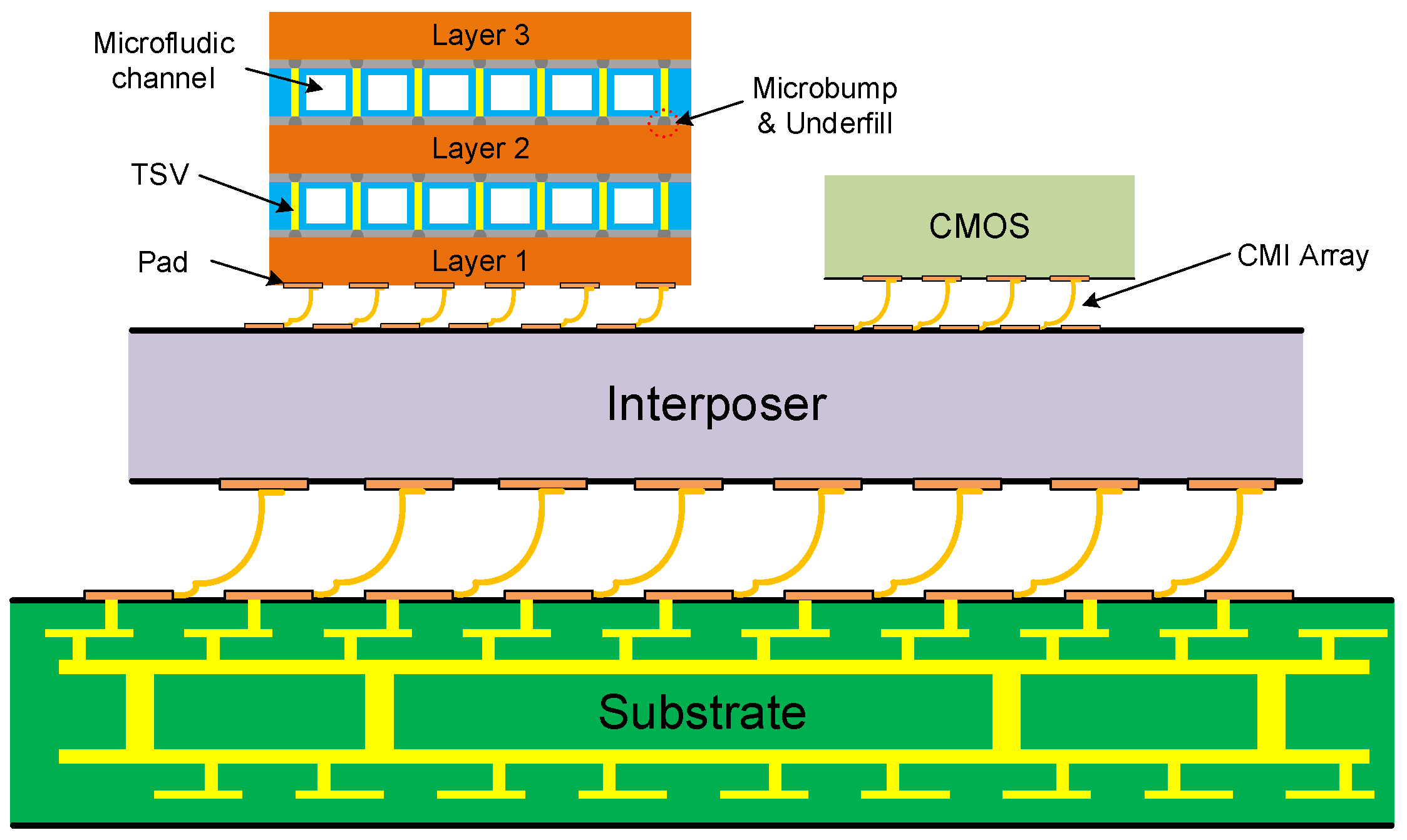
:1. Introduction
- The contact plane of the reported compliant structure is usually horizontal without loading, i.e., only the edges of the plane contact with the pad, which causes small contact area and large contact resistance;
- The interconnect resistance plays a critical role in IR drop. Due to the large contact resistance between the compliant structure and the pad, a large array should be arranged to meet the IR drop threshold, which would lead to an increased package size;
- The self-heating effect caused by the large contact resistance at the interface would further enlarge the contact resistance and degrade the system power supply. At the same time, the rising temperature would increase the risk of noise mixing, thereby disturbing the purity of the supplied current;
- Until now, the reported works mainly focused on the modeling, fabrication process, and parameter measurement of compliant interconnect structures. The mechanical simulation was employed to predict and evaluate the performance of designed structures [19,20]. However, due to the significant increase in power density in 3D IC, the influence of self-heating effect on the interconnect performance cannot be ignored. Multiphysics coupling simulation should be employed to precisely evaluate the performance of compliant interconnect structure.
2. Modeling and Optimal Design Approach
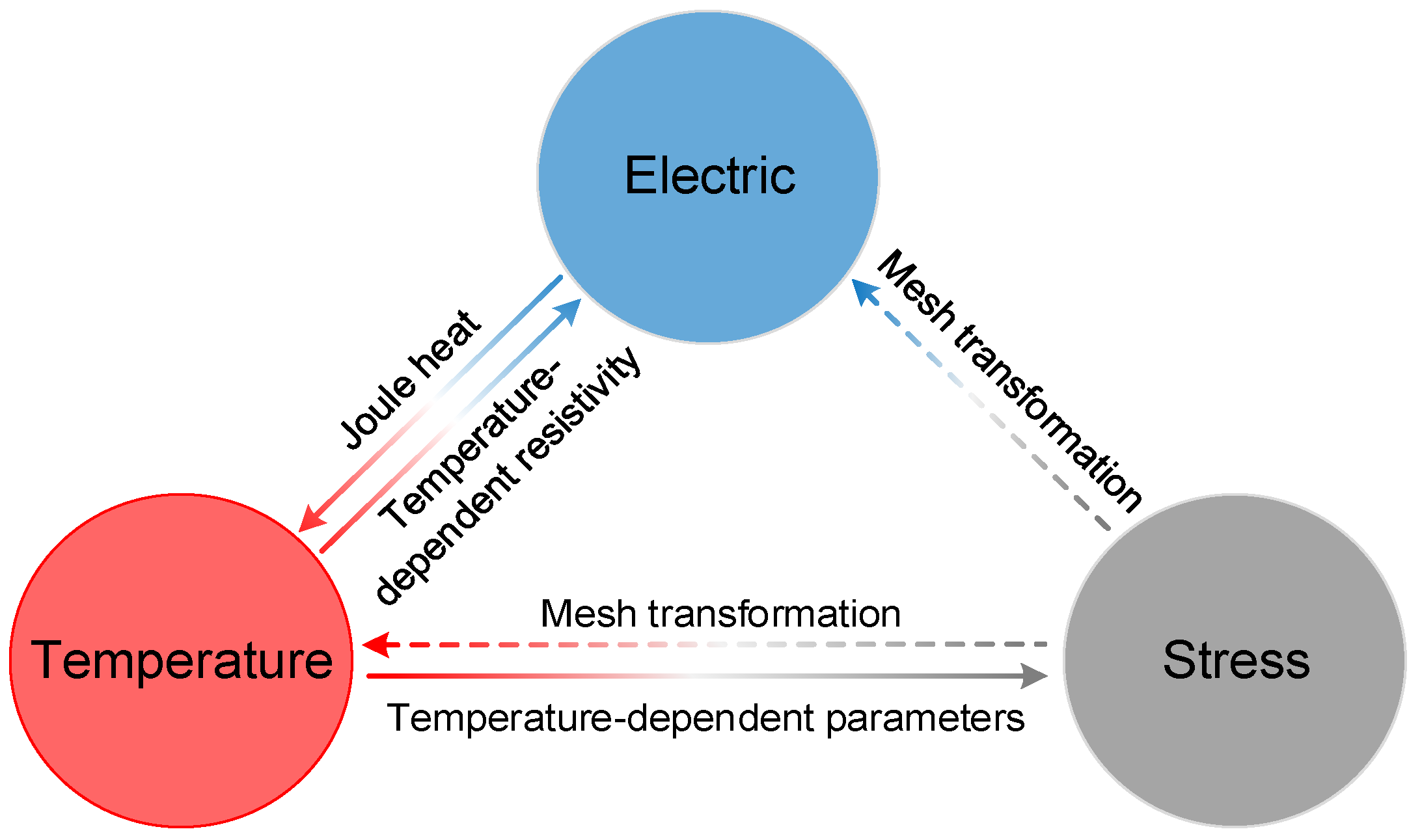
2.1. Mathematic Model for Multiphysics
2.2. Calculation of Contact Resistance
2.3. PSO Approach
| Algorithm 1: The procedure of PSO. |
| 1: Initial(); \\ Parameters definition |
| 2: for 1: Np \\ Initialization of all particles’ position and velocity |
| 3: Position random distribution(); |
| 4: Velocity random distribution(); |
| 5: Calculation of fitness function value(); |
| 6: Optimal value record(); |
| 7: end |
| 8: |
| 9: for 1: Nm |
| 10: for 1: Np |
| 11: Velocity renew(); \\ formula (3) |
| 12: Position renew(); \\ formula (4) |
| 13: Calculation of fitness function value(); |
| 14: Optimal value record(); \\ and |
| 15: end |
| 16: end |
2.4. Optimal Design Approach
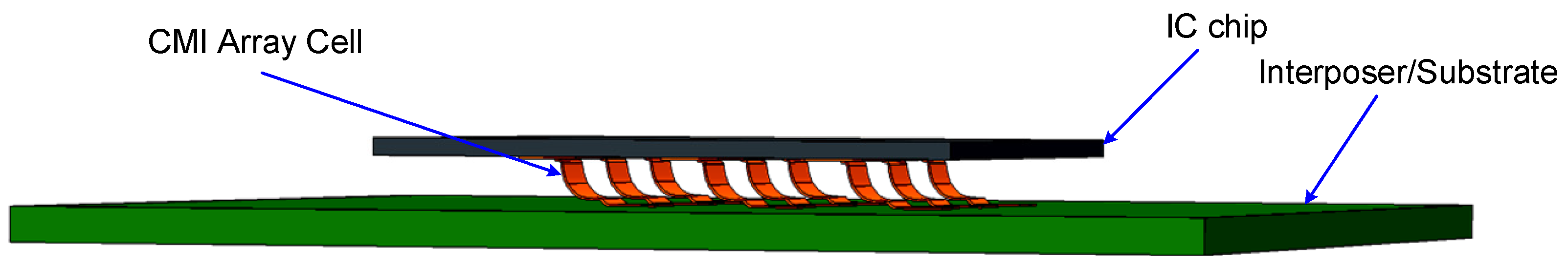
3. Modeling and Initial Simulation
3.1. Geometric Modeling
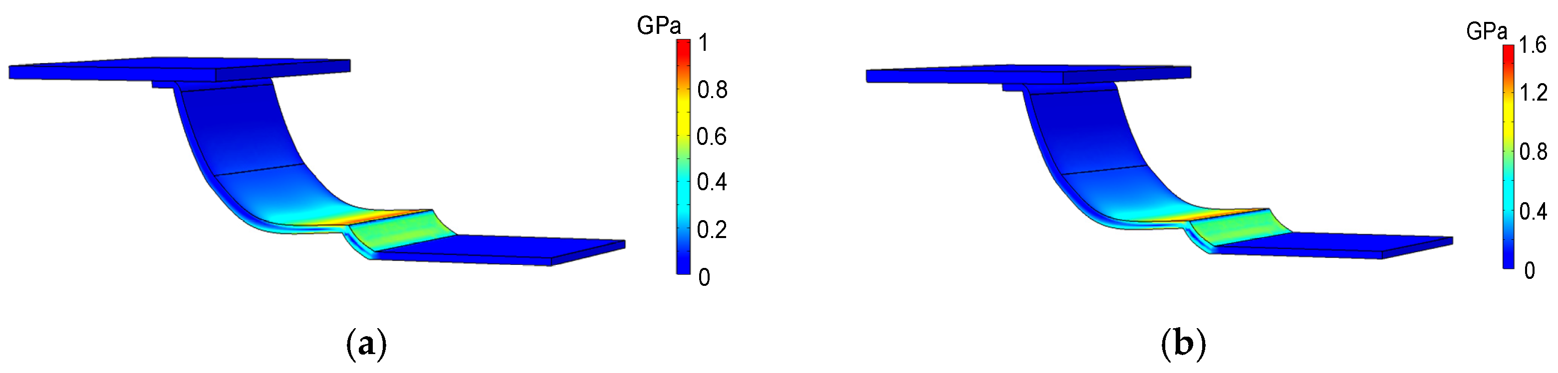
3.2. Mechanical Simulation
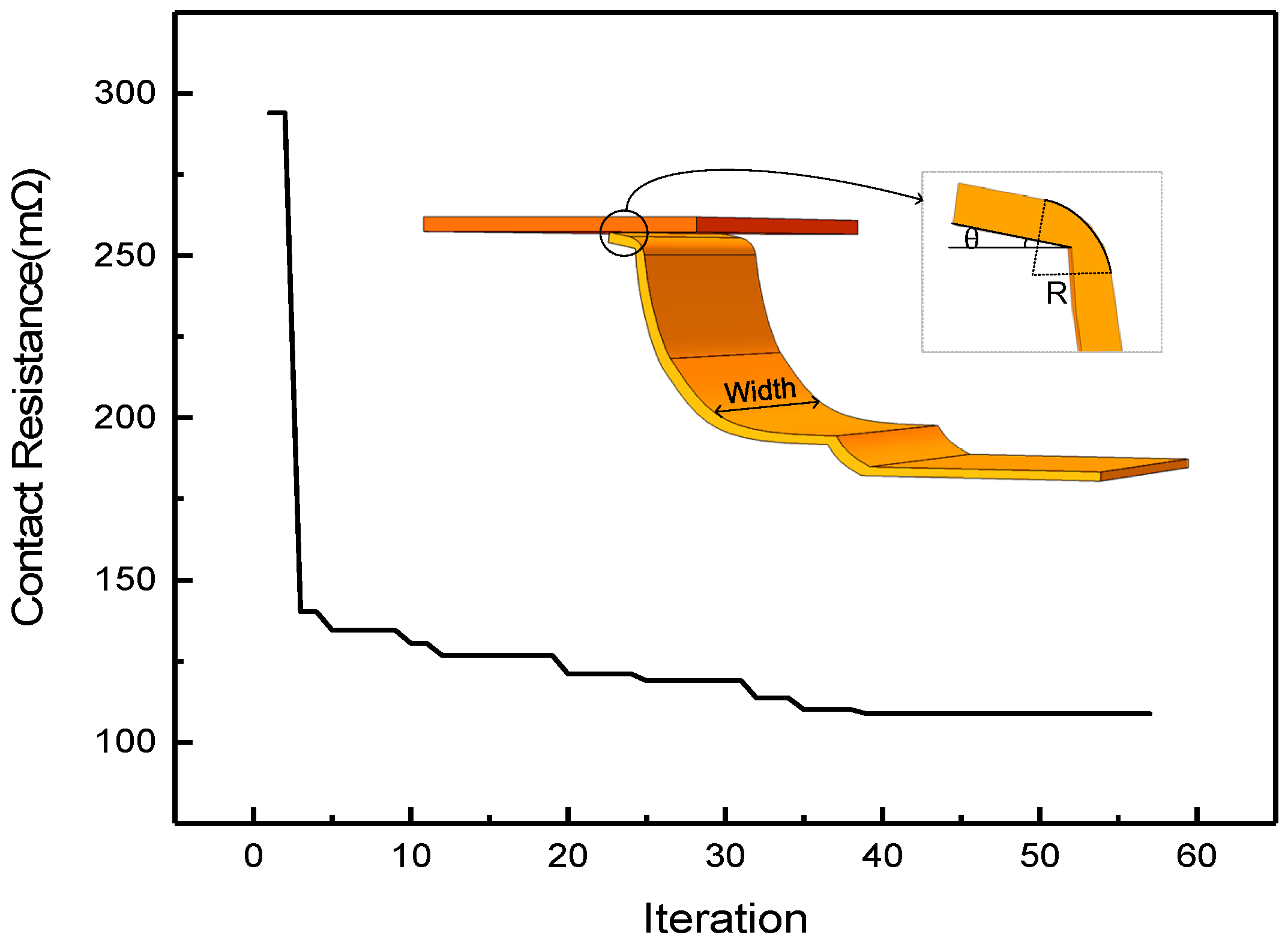
4. Parameters Optimization and Results
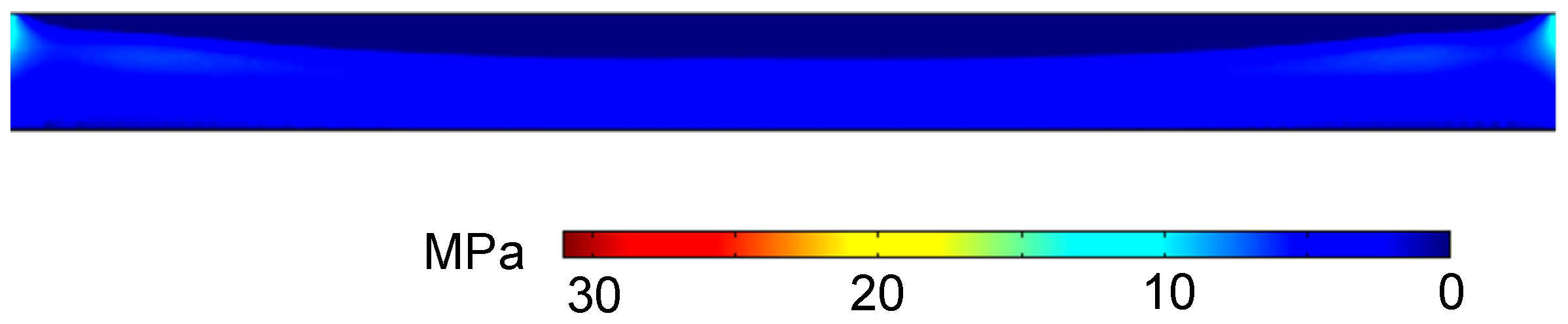
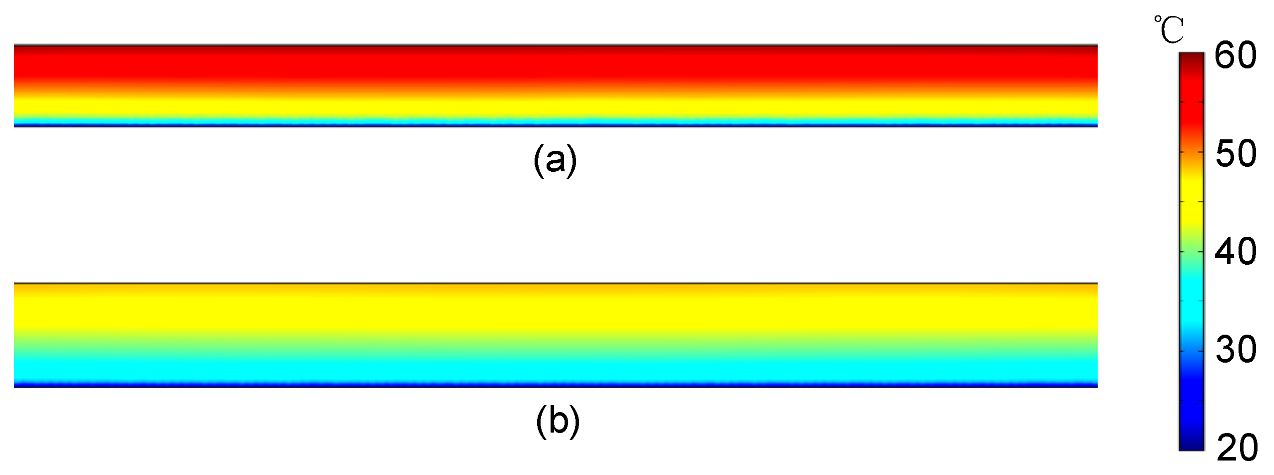
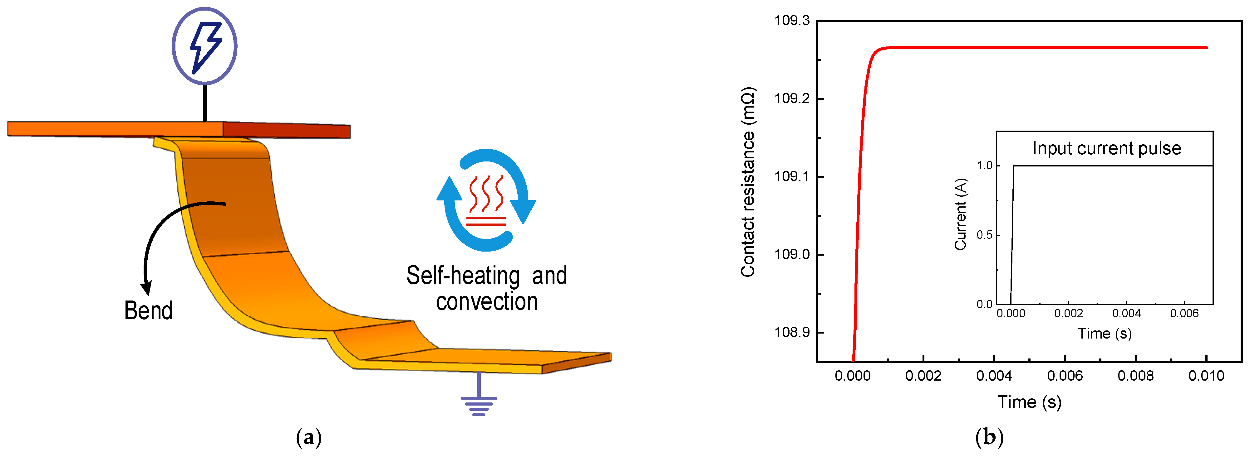
5. Multiphysics Coupling Simulation and Results
6. Conclusions
Author Contributions
Funding
Conflicts of Interest
References
- Cunningham, J.E.; Krishnamoorthy, A.V.; Shubin, I.; Zheng, X.; Asghari, M.; Feng, D.; Mitchell, J.G. Aligning chips face-to-face for dense capacitive and optical communication. IEEE Trans. Adv. Packag. 2010, 33, 389–397. [Google Scholar] [CrossRef]
- Ni, T.; Chang, H.; Song, T.; Xu, Q.; Huang, Z.; Liang, H.; Yan, A.; Wen, X. Non-Intrusive Online Distributed Pulse Shrinking-Based Interconnect Testing in 2.5D IC. IEEE Trans. Circuits Syst. II Express Briefs 2020, 67, 2657–2661. [Google Scholar] [CrossRef]
- Corbin, J.S.; Ramirez, C.N.; Massey, D.E. Land grid array sockets for server applications. IBM J. Res. Dev. 2002, 46, 763–778. [Google Scholar] [CrossRef]
- Xie, J.; Hillman, C.; Sandborn, P.; Pecht, M.G.; Hassanzadeh, A.; DeDonato, D. Assessing the operating reliability of land grid array elastomer sockets. IEEE Trans. Compon. Packag. Technol. 2000, 23, 171–176. [Google Scholar] [CrossRef]
- Yang, S.; Wu, J.; Pecht, M.G. Reliability assessment of land grid array sockets subjected to mixed flowing gas environment. IEEE Trans. Reliab. 2009, 58, 634–640. [Google Scholar] [CrossRef]
- Yang, S.; Wu, J.; Tasi, D.; Pecht, M.G. Contact resistance estimation for time-dependent silicone elastomer matrix of land grid array socket. IEEE Trans. Compon. Packag. Technol. 2007, 30, 81–85. [Google Scholar] [CrossRef]
- Ezzouine, Z.; Danovitch, D.; Bechou, L.; Pioro-Ladrière, M.; Lacerte, M. Contact Resistance Behavior of Land Grid Array Sockets at Cryogenic Temperatures Required for Quantum Measurements. IEEE. Trans. Compon. Packag. Manuf. Technol. 2021, 11, 367–374. [Google Scholar] [CrossRef]
- Reed, H.A.; Bakir, M.S.; Patel, C.S.; Martin, K.P.; Meindl, J.D.; Kohl, P.A. Compliant wafer level package (CWLP) with embedded air-gaps for sea of leads (SoL) interconnections. In Proceedings of the IEEE 2001 International Interconnect Technology Conference (Cat. No.01EX461), Burlingame, CA, USA, 6 June 2001; pp. 151–153. [Google Scholar] [CrossRef]
- Bakir, M.S.; Dang, B.; Emery, R.; Vandentop, G.; Kohl, P.A.; Meindl, J.D. Sea of leads compliant I/O interconnect process integration for the ultimate enabling of chips with low-k interlayer dielectrics. IEEE Trans. Adv. Packag. 2005, 28, 488–494. [Google Scholar] [CrossRef]
- Kacker, K.; Sitaraman, S.K. Electrical/Mechanical Modeling, Reliability Assessment, and Fabrication of FlexConnects: A MEMS-Based Compliant Chip-to-Substrate Interconnect. J. Microelectromech. Syst. 2009, 18, 322–331. [Google Scholar] [CrossRef]
- Zhang, C.; Yang, H.S.; Bakir, M.S. Highly Elastic Gold Passivated Mechanically Flexible Interconnects. IEEE Trans. Compon. Packag. Manuf. Technol. 2013, 3, 1632–1639. [Google Scholar] [CrossRef]
- Zhang, C.; Yang, H.S.; Thacker, H.D.; Shubin, I.; Cunningham, J.E.; Bakir, M.S. Mechanically flexible interconnects with contact tip for rematable heterogeneous system integration. IEEE Trans. Compon. Packag. Manuf. Technol. 2016, 6, 1587–1594. [Google Scholar] [CrossRef]
- Gonzalez, J.L.; Jo, P.K.; Abbaspour, R.; Bakir, M.S. Flexible Interconnect Design Using a Mechanically-Focused, Multi-Objective Genetic Algorithm. J. Microelectromech. Syst. 2018, 27, 677–685. [Google Scholar] [CrossRef]
- Zhang, Y.; Zhang, Y.; Bakir, M.S. Thermal Design and Constraints for Heterogeneous Integrated Chip Stacks and Isolation Technology Using Air Gap and Thermal Bridge. IEEE Trans. Comp. Packag. Manufac. Technol. 2014, 4, 1914–1924. [Google Scholar] [CrossRef]
- Zhang, Y.; Zhang, Y.; Sarvey, T.; Zhang, C.; Zia, M.; Bakir, M. Thermal Isolation Using Air Gap and Mechanically Flexible Interconnects for Heterogeneous 3-D ICs. IEEE Trans. Comp. Packag. Manufac. Technol. 2016, 6, 31–39. [Google Scholar] [CrossRef]
- Jo, P.K.; Zhang, X.; Gonzalez, J.L.; Oh, H.; Bakir, M.S. Heterogeneous multi-die stitching enabled by fine-pitch and multi-height compressible microinterconnects (CMIs). IEEE Trans. Electron Devices 2018, 65, 2957–2963. [Google Scholar] [CrossRef]
- Jo, P.K.; Rajan, S.K.; Gonzalez, J.L.; Bakir, M.S. Polylithic integration of 2.5-D and 3-D chiplets enabled by multi-height and fine-pitch CMIs. IEEE Trans. Comp. Packag. Manufac. Technol. 2020, 10, 1474–1481. [Google Scholar] [CrossRef]
- Jo, P.K.; Zia, M.; Gonzalez, J.L.; Oh, H.; Bakir, M.S. Design, fabrication, and characterization of dense compressible microinterconnects. IEEE Trans. Comp. Packag. Manufac. Technol. 2017, 7, 1003–1010. [Google Scholar] [CrossRef]
- Petrosyants, K.O.; Ryabov, N.I. Quasi-3D Thermal Simulation of Integrated Circuit Systems in Packages. Energies 2020, 13, 3054. [Google Scholar] [CrossRef]
- Filipovic, L.; Selberherr, S. Thermo-Electro-Mechanical Simulation of Semiconductor Metal Oxide Gas Sensors. Materials 2019, 12, 2410. [Google Scholar] [CrossRef] [PubMed] [Green Version]
- Bagwell, R.M.; Wetherhold, R.C. Fiber pullout behavior and impact toughness of short shaped copper fibers in thermoset matrices. Compos. Part A 2005, 36, 683–690. [Google Scholar] [CrossRef]
- Wang, S.; Fang, H.; Su, B.; Zhai, G. Method for calculation of contact resistance and finite element simulation of contact temperature rise based on rough surface contact model. In Proceedings of the 26th International Conference on Electrical Contacts, Beijing, China, 14–17 May 2012. [Google Scholar] [CrossRef]
- COMSOL Multiphysics. Available online: http://cn.comsol.com/model/contact-switch-4119 (accessed on 25 April 2021).
- Miao, K.; Feng, Q.; Kuang, W. Particle Swarm Optimization Combined with Inertia-Free Velocity and Direction Search. Electronics 2021, 10, 597. [Google Scholar] [CrossRef]
- Slavcheva, E.; Mokwa, W.; Schnakenberg, U. Electrodeposition and properties of NiW films for MEMS application. Electrochim. Acta 2005, 50, 5573–5580. [Google Scholar] [CrossRef]


| Property | Gold | Copper | NiW | Silicon |
|---|---|---|---|---|
| Density (kg/m3) | 19,300 | 8960 | 9009 | 2329 |
| Poisson’s ratio | 0.44 | 0.34 | 0.31 | 0.28 |
| Young’s module (GPa) | 70 | 120 | 180 | 170 |
| Heat conductivity coefficient (W/m·K) | 317 | 401 | 91.57 | 130 |
| Heat capacity (J/kg·K) | 129 | 384 | 441 | 700 |
| Coefficient of heat expansion (×10−6 1/K) | 14.2 | 16.5 | 13.3 | 2.6 |
| Conductivity (×106 S/m) | 45.6 | 57.1 | 3.45 | \ |
| Width (μm) | R (μm) | Slope (tanθ) | Contact Resistance (mΩ) | |
|---|---|---|---|---|
| Initial | 100 | 7 | 0.2 | 155.3 |
| Optimized | 117.4001 | 1.99 | 0.1915 | 108.8 |
| Stress (GPa) | Contact Pressure (MPa) | Contact Resistance (mΩ) | |
|---|---|---|---|
| Without | 1.66 | 40.5 | 108.8 |
| With | 1.64 | 42.1 | 109.27 |
Publisher’s Note: MDPI stays neutral with regard to jurisdictional claims in published maps and institutional affiliations. |
© 2021 by the authors. Licensee MDPI, Basel, Switzerland. This article is an open access article distributed under the terms and conditions of the Creative Commons Attribution (CC BY) license (https://creativecommons.org/licenses/by/4.0/).
Share and Cite
Zhang, P.; Wang, D.-W.; Zhao, W.-S.; Su, J.; You, B.; Liu, J. Multiphysics Analysis and Optimal Design of Compressible Micro-Interconnect for 2.5D/3D Heterogeneous Integration. Electronics 2021, 10, 2240. https://doi.org/10.3390/electronics10182240
Zhang P, Wang D-W, Zhao W-S, Su J, You B, Liu J. Multiphysics Analysis and Optimal Design of Compressible Micro-Interconnect for 2.5D/3D Heterogeneous Integration. Electronics. 2021; 10(18):2240. https://doi.org/10.3390/electronics10182240
Chicago/Turabian StyleZhang, Peng, Da-Wei Wang, Wen-Sheng Zhao, Jiangtao Su, Bin You, and Jun Liu. 2021. "Multiphysics Analysis and Optimal Design of Compressible Micro-Interconnect for 2.5D/3D Heterogeneous Integration" Electronics 10, no. 18: 2240. https://doi.org/10.3390/electronics10182240