
A Proposal of Vertical MOSFET and Electrothermal Analysis for Monolithic 3-D ICs


Abstract
:1. Introduction
2. Modeling
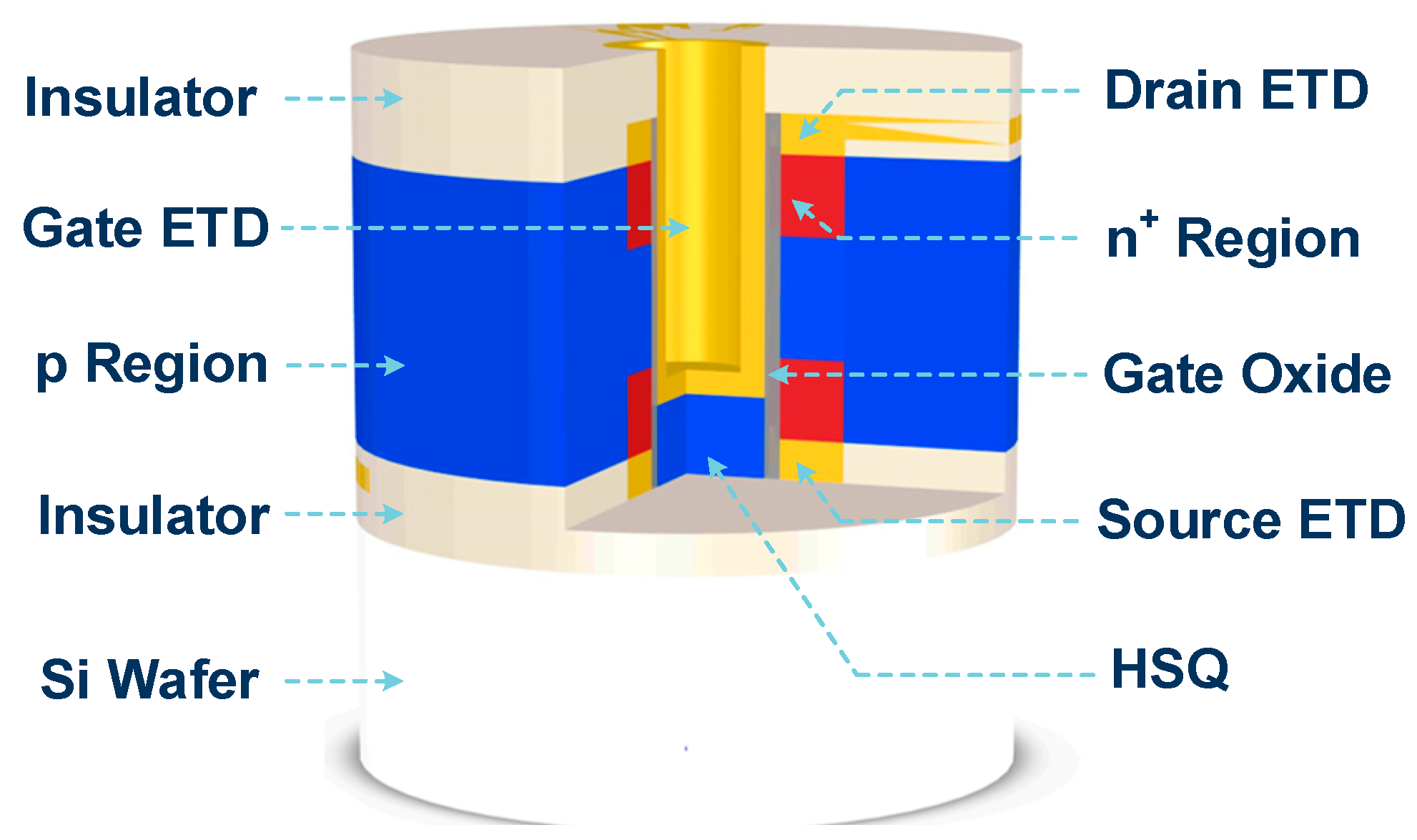
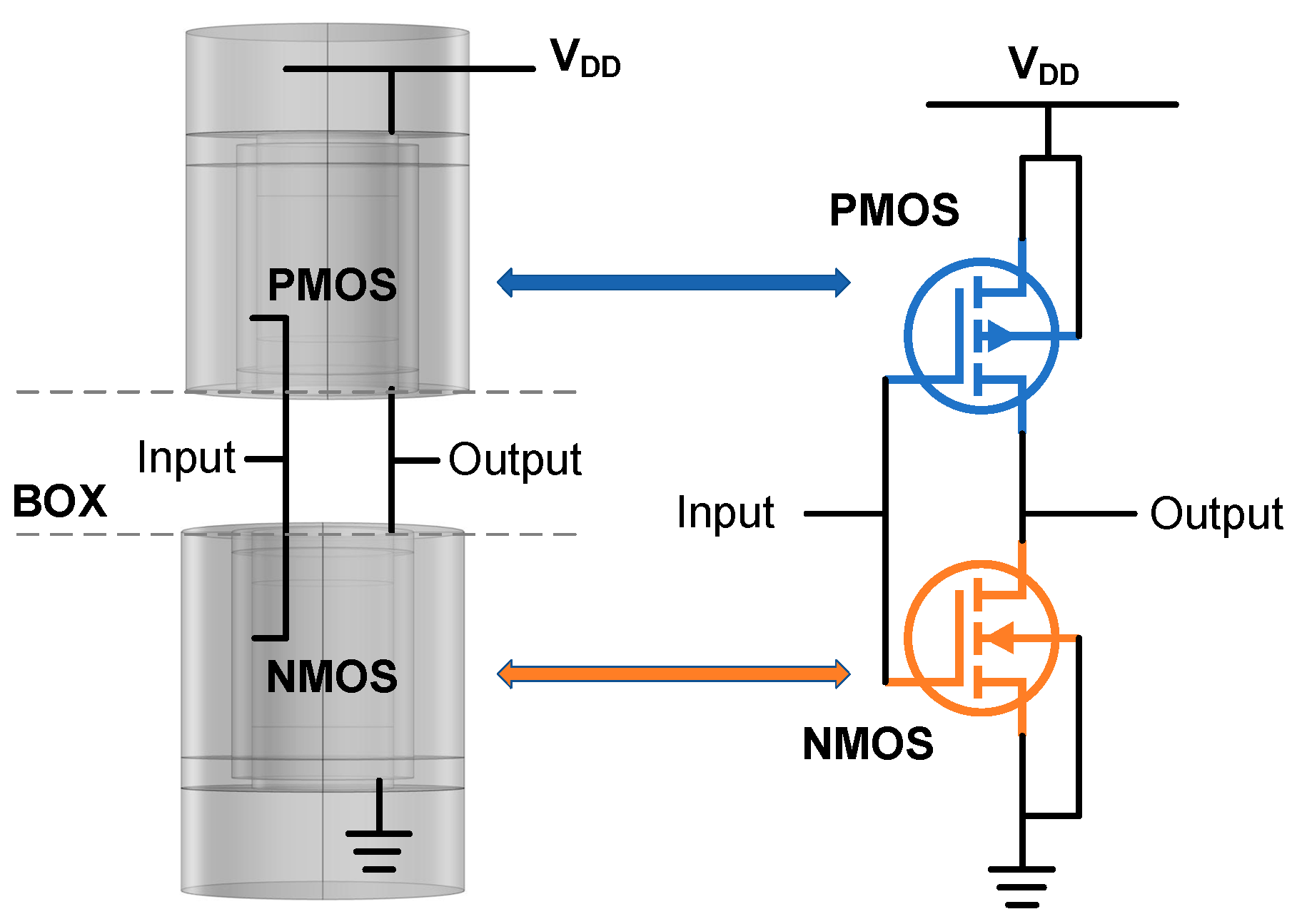
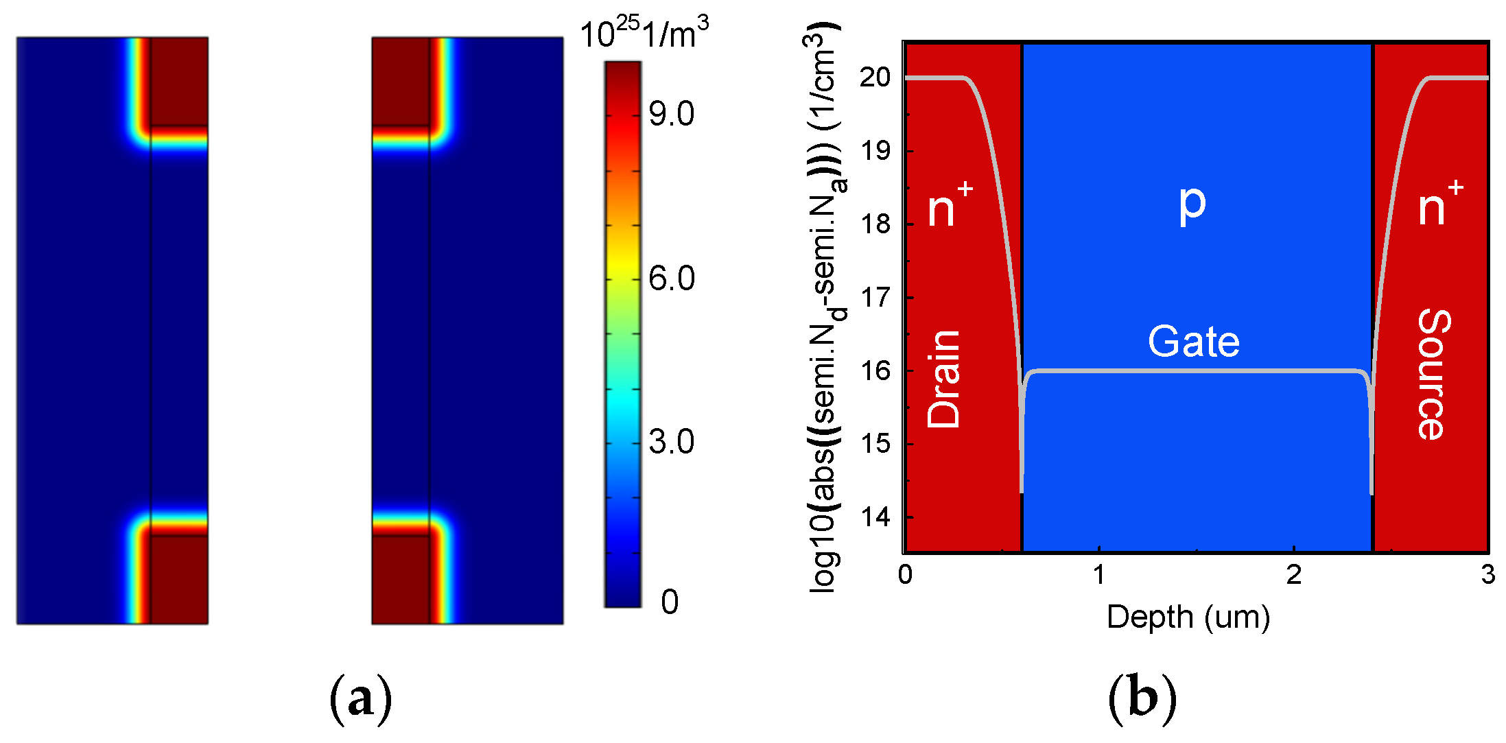
2.1. Device Model
2.2. Fabrication Process
3. Simulation
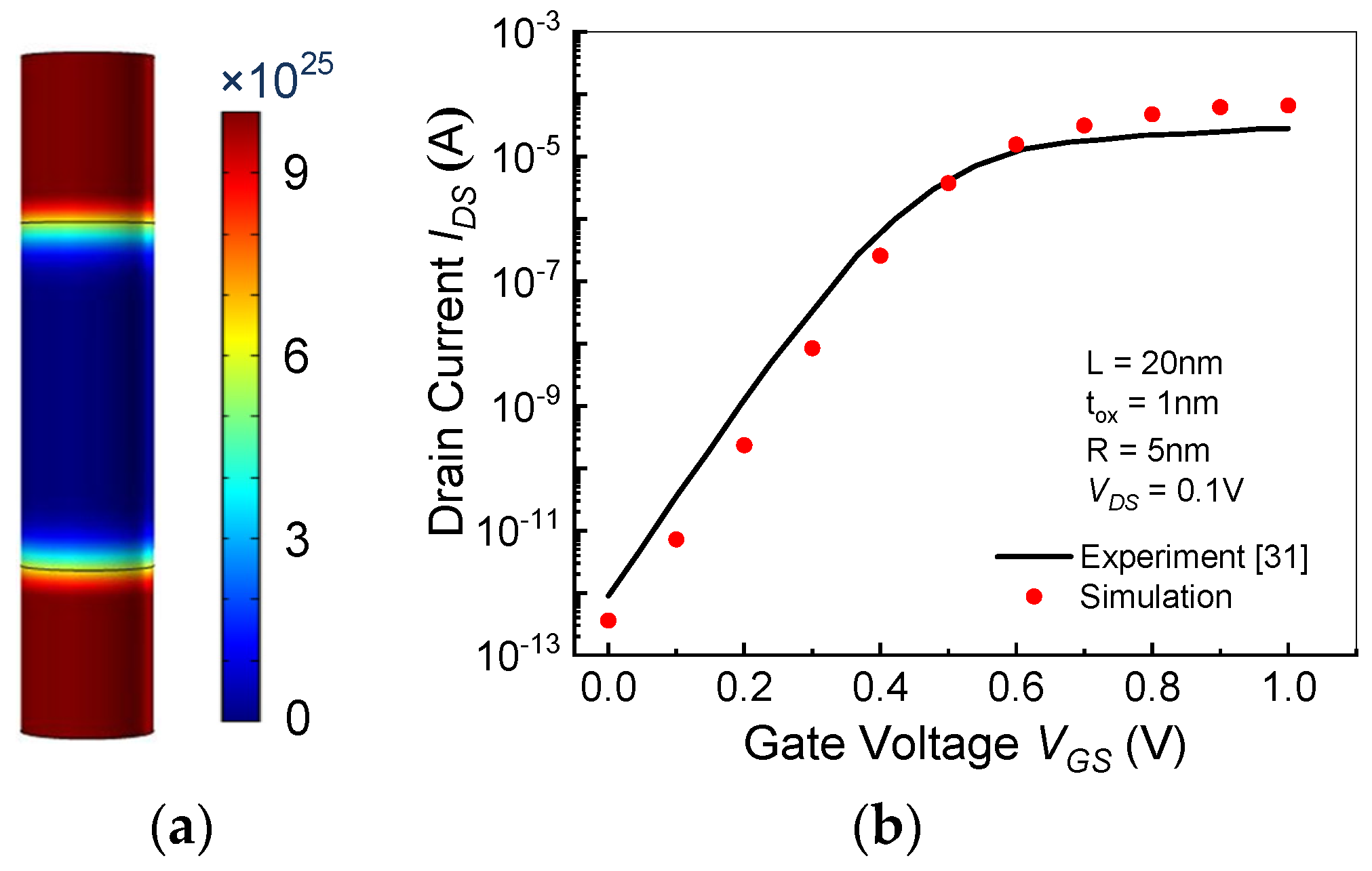
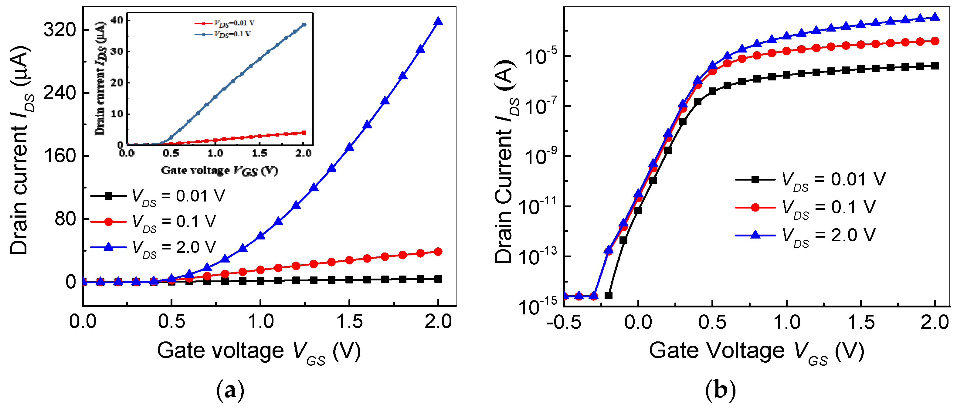
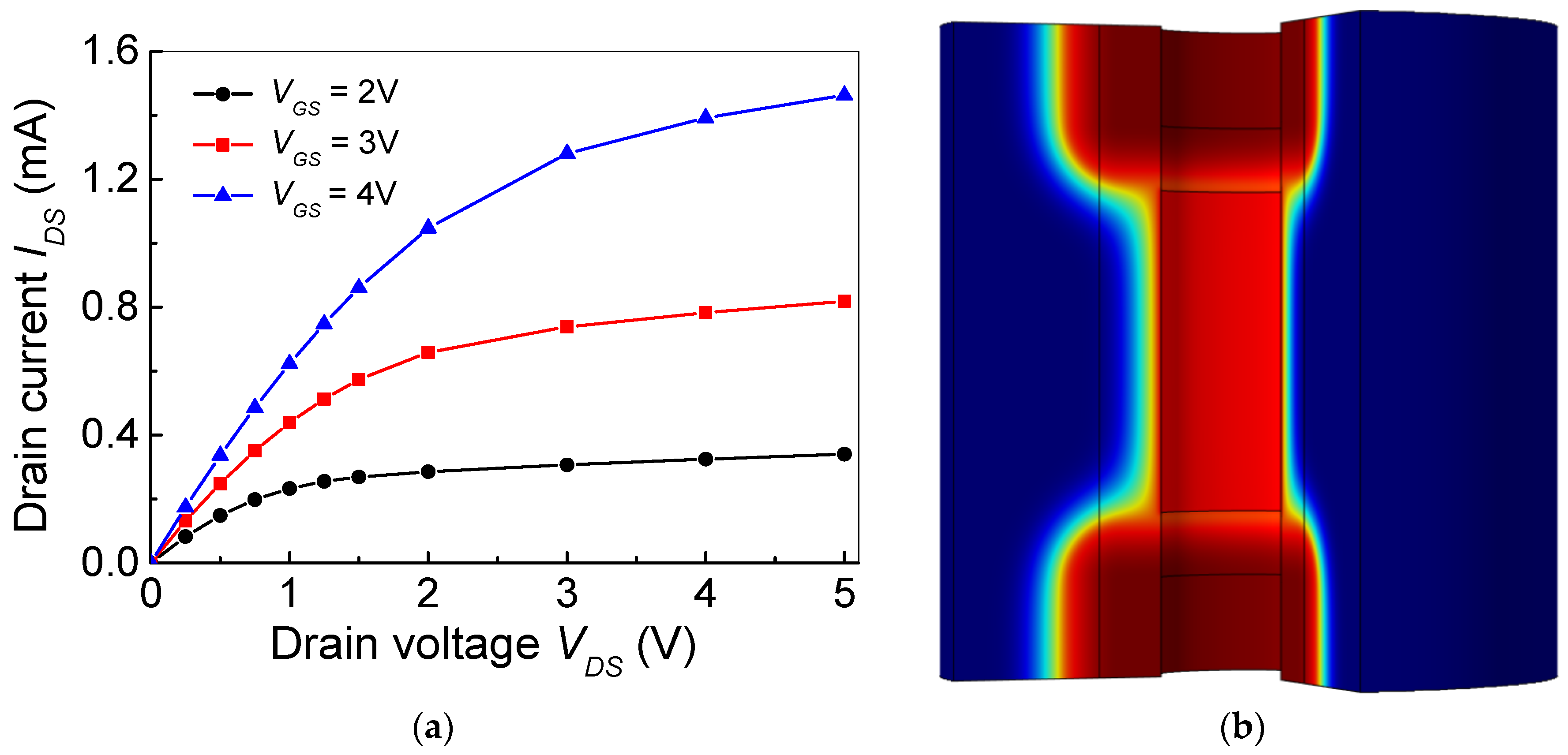
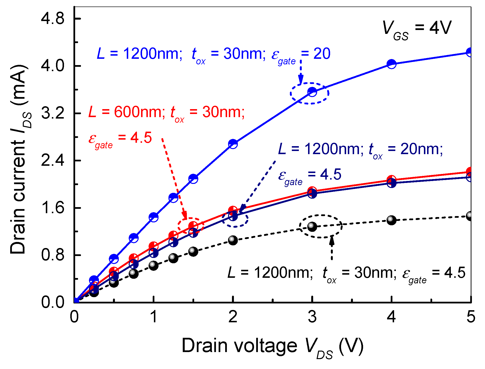
3.1. Electrical Performance
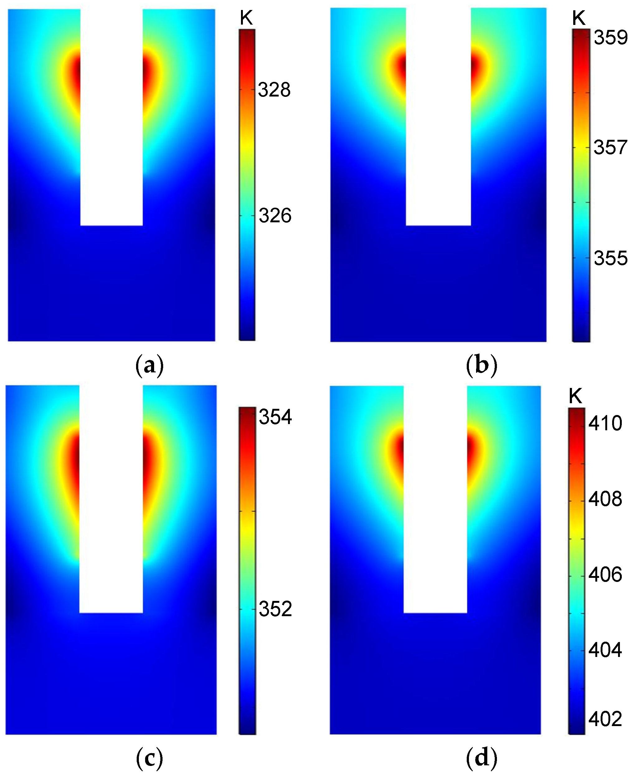
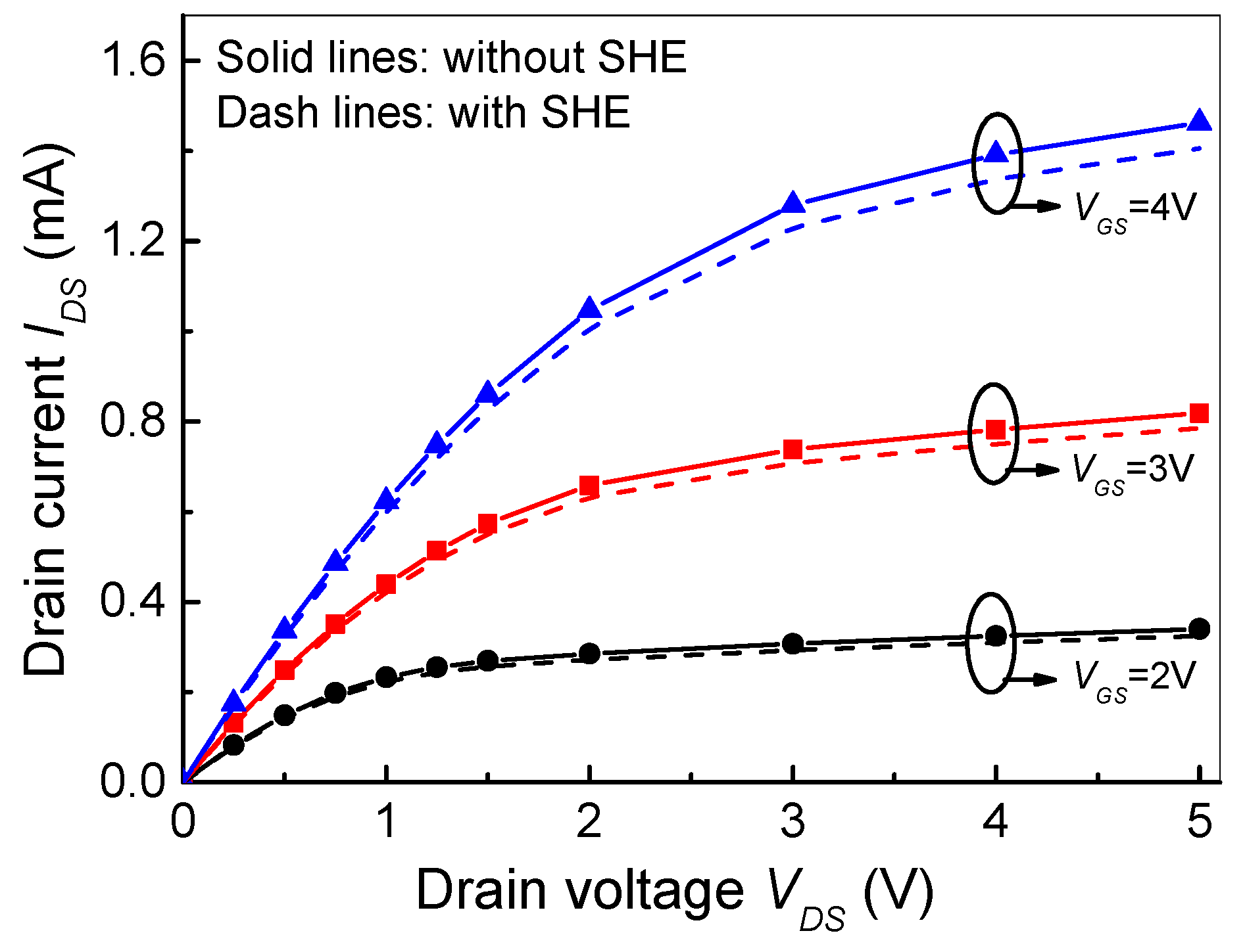
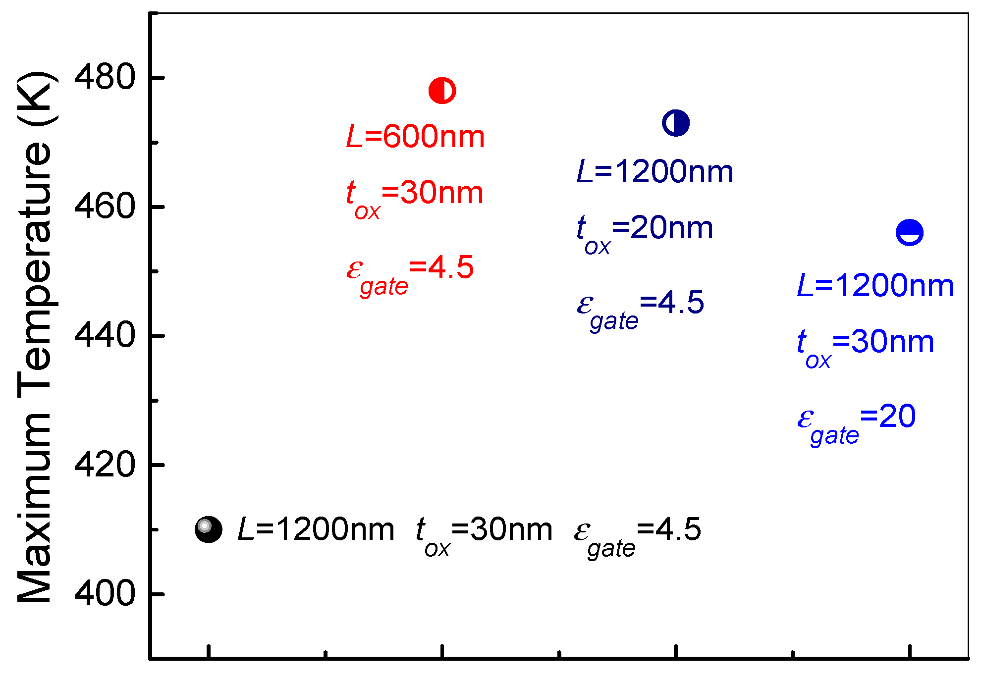
3.2. Electrothermal Coupling Simulation
4. Results and Discussion
5. Conclusions
Author Contributions
Funding
Informed Consent Statement
Conflicts of Interest
References
- Fleetwood, D.M. Evolution of total ionizing dose effects in MOS devices with Moore’s law scaling. IEEE Trans. Nucl. Sci. 2018, 65, 1465–1481. [Google Scholar] [CrossRef]
- Pourghaderi, M.A.; Pham, A.-T.; Ilatikhameneh, H.; Kim, J.; Park, H.-H.; Jin, S.; Chung, W.-Y.; Choi, W.; Maeda, S.; Lee, K.-H. Universality of short-channel effects on ultrascaled MOSFET performance. IEEE Electron Device Lett. 2018, 39, 168–171. [Google Scholar] [CrossRef]
- Hu, X.; Stow, D.; Xie, Y. Die stacking is happening. IEEE Micro 2018, 38, 22–28. [Google Scholar] [CrossRef]
- Guler, A.; Jha, N.K. McPAT-Monolithic: An area/power/timing architecture modeling framework for 3-D hybrid monolithic multicore systems. IEEE Trans. Very Large Scale Integr. (VLSI) Syst. 2020, 28, 2146–2156. [Google Scholar] [CrossRef]
- Lee, Y.; Lim, S.K. Ultrahigh density logic designs using monolithic 3-D integration. IEEE Trans. Comput. Aided Des. Integr. Circuits Syst. 2013, 32, 1892–1905. [Google Scholar] [CrossRef]
- Berg, M.; Kilpi, O.-P.; Persson, K.-M.; Svensson, J.; Hellenbrand, M.; Lind, E.; Wernersson, L.-E. Electrical characterization and modeling of gate-last vertical InAs nanowire MOSFETs on Si. IEEE Electron Device Lett. 2016, 37, 966–969. [Google Scholar] [CrossRef] [Green Version]
- Donaghy, D.; Hall, S.; de Groot, C.H.; Kunz, D.V.; Ashburn, P. Design of 50-nm vertical MOSFET incorporating a dielectric pocket. IEEE Trans. Electron Devices 2004, 51, 158–161. [Google Scholar] [CrossRef]
- Gandhi, R.; Chen, Z.; Singh, N.; Banerjee, K.; Lee, S. Vertical Si-nanowire n-type tunneling FETs with low subthreshold swing (≤50 mV/decade) at room temperature. IEEE Electron Device Lett. 2011, 32, 437–439. [Google Scholar] [CrossRef]
- Zhao, X.; Heidelberger, C.; Fitzgerald, E.A.; del Alamo, J.A. Source/drain asymmetry in InGaAs vertical nanowire MOSFETs. IEEE Trans. Electron Devices 2017, 64, 2161–2165. [Google Scholar] [CrossRef]
- Zheng, P.; Connelly, D.; Ding, F.; Liu, T.K. FinFET evolution toward stacked-nanowire FET for CMOS technology scaling. IEEE Trans. Electron Devices 2015, 62, 3945–3950. [Google Scholar] [CrossRef]
- Johansson, S.; Egard, M.; Ghalamestani, S.G.; Borg, B.M.; Berg, M.; Wernersson, L.-E.; Lind, E. RF characterization of vertical InAs nanowire wrap-gate transistors integrated on Si substrates. IEEE Trans. Microw. Theory Tech. 2011, 59, 2733–2738. [Google Scholar] [CrossRef] [Green Version]
- Lyu, X.; Chen, X. Vertical power Hk-MOSFET of hexagonal layout. IEEE Trans. Electron Devices 2013, 60, 1709–1715. [Google Scholar] [CrossRef]
- Ji, D.; Gupta, C.; Agarwal, A.; Chan, S.H.; Lund, C.; Li, W.; Keller, S.; Mishra, U.K.; Chowdhury, S. Large-area in-situ oxide, GaN interlayer-based vertical trench MOSFET (OG-FET). IEEE Electron Device Lett. 2018, 39, 711–714. [Google Scholar] [CrossRef]
- Sharma, R.; Rathore, R.S.; Rana, A.K. Impact of high-k spacer on device performance of nanoscale underlap fully depleted SOI MOSFET. J. Circuits Syst. Comput. 2017, 27, 1850063-1–1850063-13. [Google Scholar] [CrossRef]
- Maity, N.P.; Maity, R.; Baishya, S. Ultrathin body partial silicon-on-insulator MOSFET with suppressed floating body effect: A simulation study. J. Nanoelectron. Optoelectron. 2017, 12, 472–479. [Google Scholar] [CrossRef]
- Yang, P.; Hook, T.B.; Oldiges, P.J.; Doris, B.B. Vertical slit FET at 7-nm node and beyond. IEEE Trans. Electron Devices 2016, 63, 3327–3334. [Google Scholar] [CrossRef]
- Larrieu, G.; Dubois, E. Schottky-barrier source/drain MOSFETs on ultrathin SOI body with a tungsten metallic midgap gate. IEEE Electron Device Lett. 2004, 25, 801–803. [Google Scholar] [CrossRef]
- Guan, L.P.; Sin, J.K.O.; Xiong, Z.B.; Liu, H.T. A novel SOI lateral-power MOSFET with a self-aligned drift region. IEEE Electron Device Lett. 2005, 26, 264–266. [Google Scholar] [CrossRef]
- Anvarifard, M.K.; Orouji, A.A. Enhanced critical electrical characteristics in a nanoscale low-voltage SOI MOSFET with dual tunnel diode. IEEE Trans. Electron Devices 2015, 62, 1672–1676. [Google Scholar] [CrossRef]
- Samal, S.K.; Panth, S.; Samadi, K.; Saeidi, M.; Du, Y.; Lim, S.K. Adaptive regression-based thermal modeling and optimization for monolithic 3-D ICs. IEEE Trans. Comput. Aided Des. Integr. Circuits Syst. 2016, 35, 1707–1720. [Google Scholar] [CrossRef]
- Zhang, L.; Song, D.; Xiao, Y.; Lin, X.; Chan, M. On the formulation of self-heating models for circuit simulation. IEEE J. Electron Devices Soc. 2018, 6, 291–297. [Google Scholar] [CrossRef]
- Xu, Y.; Ho, C.N.M.; Ghosh, A.; Muthumuni, D. Design, Implementation, and Validation of Electro-Thermal Simulation for SiC MOSFETs in Power Electronic Systems. IEEE Trans. Ind. Appl. 2021, 57, 2714–2725. [Google Scholar] [CrossRef]
- COMSOL Multiphysics. Available online: http://cn.comsol.com/blogs/how-to-perform-a-3d-analysis-of-a-semiconductor-device/ (accessed on 25 April 2021).
- Saxena, P.; Gorji, N.E. COMSOL simulation of heat distribution in perovskite solar cells: Coupled optical–electrical–thermal 3-D analysis. IEEE J. Photovolt. 2019, 9, 1693–1698. [Google Scholar] [CrossRef]
- Jia, Y.; Xiao, F.; Duan, Y.; Luo, Y.; Liu, B.; Huang, Y. PSpice-COMSOL-Based 3-D Electrothermal–Mechanical Modeling of IGBT Power Module. IEEE J. Emerg. Sel. Top. Power Electron. 2020, 8, 4173–4185. [Google Scholar] [CrossRef]
- Zhou, H.; Alghmadi, S.; Si, M.; Qiu, G.; Ye, P.D. Al2O3/β-Ga2O3 (-201) interface improvement through piranha pretreatment and postdeposition annealing. IEEE Electron Device Lett. 2016, 37, 1411–1414. [Google Scholar] [CrossRef]
- Ohara, J.; Kano, K.; Takeuchi, Y.; Ohya, N.; Otsuka, Y.; Akita, S. A new deep reactive ion etching process by dual sidewall protection layer. In Proceedings of the IEEE Thirteenth Annual International Conference on Micro Electro Mechanical Systems (Cat. No.00CH36308), Miyazaki, Japan, 23–27 January 2000; pp. 277–282. [Google Scholar]
- Winkler, F.; Killge, S.; Fischer, D.; Richter, K.; Hiess, A.; Bartha, J.W. TSV transistor—Vertical metal gate FET inside a through silicon via. IEEE Electron Device Lett. 2018, 39, 1493–1496. [Google Scholar] [CrossRef]
- Memišević, E.; Lind, E.; Wernersson, L.E. Thin electron beam defined hydrogen silsesquioxane spacers for vertical nanowire transistors. J. Vac. Sci. Technol. B 2014, 32, 051211-1–051211-6. [Google Scholar] [CrossRef] [Green Version]
- Son, D.; Myeong, I.; Kim, H.; Kang, M.; Jeon, J.; Shin, H. Analysis of electrothermal characteristics of GAA vertical nanoplate-shaped FETs. IEEE Trans. Electron Devices 2018, 65, 3061–3064. [Google Scholar] [CrossRef]
- Belkhiria, M.; Echouchene, F.; Jaba, N.; Bajahzar, A.; Belmabrouk, H. 2-D-Nonlinear Electrothermal Model for Investigating the Self-Heating Effect in GAAFET Transistors. IEEE Trans. Electron Devices 2021, 68, 954–961. [Google Scholar] [CrossRef]
- Fjeldly, T.A.; Shur, M. Threshold voltage modeling and the subthreshold regime of operation of short-channel MOSFETs. IEEE Trans. Electron Devices 1993, 40, 137–145. [Google Scholar] [CrossRef]
- Liu, M.; Lentz, F.; Trellenkamp, S.; Hartmann, J.-M.; Knoch, J.; Grutzmacher, D.; Buca, D.; Zhao, Q.-T. Diameter scaling of vertical Ge gate-all-around nanowire pMOSFETs. IEEE Trans. Electron Devices 2020, 67, 2988–2994. [Google Scholar] [CrossRef]
- Thingujam, T.; Dai, Q.; Kim, E.; Lee, J.-H. A simulation study on the effects of interface charges and geometry on vertical GAA GaN nanowire MOSFET for low-power application. IEEE Access 2021, 9, 101447–101453. [Google Scholar] [CrossRef]
- Vudumula, P.; Kotamraju, S. Design and optimization of SiC super-junction MOSFET using vertical variation doping profile. IEEE Trans. Electron Devices 2019, 66, 1402–1408. [Google Scholar] [CrossRef]
- Hsu, P.; Chen, H.; Hwang, T. Stacking Signal TSV for thermal dissipation in global routing for 3-D IC. IEEE Trans. Comput. Aided Des. Integr. Circuits Syst. 2014, 33, 1031–1042. [Google Scholar]
- Zhou, W.; Zhong, X.; Sheng, K. High temperature stability and the performance degradation of SiC MOSFETs. IEEE Trans. Power Electron. 2014, 29, 2329–2337. [Google Scholar] [CrossRef]
- Chen, T.P.; Huang, J.Y.; Tse, M.S.; Tan, S.S.; Ang, C.H. Gate oxide thickness dependence of edge charge trapping in NMOS transistors caused by charge injection under constant-current stress. IEEE Trans. Electron Devices 2003, 50, 1548–1550. [Google Scholar] [CrossRef]


| VDS (V) | Ion/Ioff Ratio | SS (mV/dec) |
|---|---|---|
| 0.01 | 1.4 109 | 69 |
| 0.1 | 1.52 1010 | 79 |
| 2 | 1.28 1011 | 81 |
Publisher’s Note: MDPI stays neutral with regard to jurisdictional claims in published maps and institutional affiliations. |
© 2021 by the authors. Licensee MDPI, Basel, Switzerland. This article is an open access article distributed under the terms and conditions of the Creative Commons Attribution (CC BY) license (https://creativecommons.org/licenses/by/4.0/).
Share and Cite
Zhu, J.-H.; Wang, D.-W.; Zhao, W.-S.; Dai, J.-Y.; Wang, G. A Proposal of Vertical MOSFET and Electrothermal Analysis for Monolithic 3-D ICs. Electronics 2021, 10, 2241. https://doi.org/10.3390/electronics10182241
Zhu J-H, Wang D-W, Zhao W-S, Dai J-Y, Wang G. A Proposal of Vertical MOSFET and Electrothermal Analysis for Monolithic 3-D ICs. Electronics. 2021; 10(18):2241. https://doi.org/10.3390/electronics10182241
Chicago/Turabian StyleZhu, Jia-He, Da-Wei Wang, Wen-Sheng Zhao, Jia-Yun Dai, and Gaofeng Wang. 2021. "A Proposal of Vertical MOSFET and Electrothermal Analysis for Monolithic 3-D ICs" Electronics 10, no. 18: 2241. https://doi.org/10.3390/electronics10182241
APA StyleZhu, J.-H., Wang, D.-W., Zhao, W.-S., Dai, J.-Y., & Wang, G. (2021). A Proposal of Vertical MOSFET and Electrothermal Analysis for Monolithic 3-D ICs. Electronics, 10(18), 2241. https://doi.org/10.3390/electronics10182241