Article

A Compact Widely Tunable Bandpass Filter Dedicated to Preselectors

Department of Electronics, Electrical Engineering and Microelectronics, Silesian University of Technology, Akademicka 16, 44-100 Gliwice, Poland
*
Author to whom correspondence should be addressed.
Electronics 2021, 10(18), 2315; https://doi.org/10.3390/electronics10182315
Submission received: 27 August 2021 / Revised: 15 September 2021 / Accepted: 18 September 2021 / Published: 21 September 2021
(This article belongs to the Section Microwave and Wireless Communications)

Abstract

:
This article presents a novel compact widely tunable bandpass filter. The filter consists of two resonators that are double-coupled, inductively, where the coupling inductances are elements of the input and output networks. The application of double-coupling enabled the transmission zero next to the upper cutoff frequency. This makes the filter useful for applications in preselector networks used in receiving systems with a low to intermediate frequency with the desired channel frequency lower than the image channel frequency. The article shows the practical realisation of the varactor-tuned example filter fabricated as a microstrip planar network of an overall size of 0.03 λ g × 0.045 λ g . The tuning range of the proposed filter is from 410 MHz to 880 MHz with the fractional bandwidth equal to 7.5–8.1% and an in-band insertion loss better than −3.4 dB. The achieved IP3 value exceeds 17.5 dBm.

1. Introduction

Bandpass filters (BPFs) are components of many RF devices and systems. They find application in many different areas including measurement devices, mobile and satellite communications, and broadcasting. In particular, the bandpass filters play a very important role as input filters (so-called preselectors) of microwave receivers where tunable and fixed centre frequency filters are used. Preselectors are implemented in order to eliminate parasitic channels and the unwanted signal leakage (e.g., heterodyne and its harmonics) through the receiver input. They are used both in frequency conversion receivers and in tuned radio frequency receivers [1]. Preselectors using BPFs can have different designs depending on the operating frequency and tuning range. Contemporary communication equipment is required to be small in size and low weight. These properties strictly depend on the size and weight of the applied filters. Therefore, varactor-tuned networks are favoured instead of YIG filters, despite the excellent properties of the latter [2].
Preselector filtering properties and its linearity (characterized by the IP3 parameter) determine the receiver immunity to intermodulation distortions caused by the signals fed from the antenna. The bandpass preselector reduces the levels of intermodulation components produced in the following blocks of the receiver, coming from the out-of-band signals. At the same time, the preselector with an insufficient value of the IP3 may become a source of intermodulation distortions due to the nonlinearity of semiconductor elements used as switches and variable reactances. Therefore, designing bandpass filters dedicated to the preselectors that are tuned with the varactors and have a wide tuning range together with a high IP3 value is a big challenge for the designer.
Tunable bandpass filters can be designed for networks with a constant absolute bandwidth (CABW) [3,4,5] or a constant fractional bandwidth (CFBW) [6,7,8,9,10,11]. In both cases, the filters should be characterized by low insertion loss in the full tuning range and adequate attenuation in the stopband, which is necessary to eliminate unwanted signals. The natural property of the transmission-line-based filter is the existence of additional higher passbands, which could be successfully adopted for multiband BPF design [12]. In other cases, the additional passbands deteriorate the stopband attenuation. This effect can be reduced by means of layout topology modification [13,14] or introducing additional transmission zeros [15,16,17,18]. The application of the transmission zero can also control the bandwidth and narrow the transition band if its frequency is close enough to the centre frequency of the filter [19]. Transmission zeros may be the inherent property of the filter [6,11] or may be the result of the application of additional resonant circuits (resonators) added to the structure [15,20]. Transmission zeros’ frequencies can be fixed [16,21], tuned independently to the filter centre frequency [22,23,24], or tuned simultaneously with the filter centre frequency [6,7,8,9,10,11].
A detailed comparison of the properties of various constructions of bandpass microstrip filters can be found in [25]. The BPF in most cases consists of a number of cascaded resonators, in which the input and output resonators are matched to the source and load impedances. In planar filters, microstrip lines [21,26], coupled microstrip lines [8,27,28], or capacitively loaded microstrip lines [29] are used as resonators. The number and type of applied resonators determine the area occupied by the network. Varactors [6,7,8,9,10,11] or MEMS capacitors [30] controlled with a common voltage [7,11,29,31] or separate independent voltages [6,8,28,32] are used as the tuning elements. Additionally, a reconfiguration of the filter network can be applied by means of the PIN diodes [33] or MEMS switches [34].
In designing microwave filters, electrical analogies between the lumped elements and transmission lines are commonly applied. This approach is effective both in the synthesis of distributed parameter filters based on the lumped element prototype [24,35,36,37,38,39] and in the analysis of the distributed element networks with the use of the equivalent lumped element circuits [15,18,40]. In both cases, a modal analysis based on determining the response to odd and even excitations is an efficient method to obtain the filter frequency properties [41,42].
One of the classic solutions of bandpass filters is a double-tuned filter consisting of two coupled resonators, e.g., two parallel resonant circuits [1]. Such a filter, despite its simple structure, has very good electrical parameters. The use of filters made of two identical resonators enables easy tuning of the passband centre frequency by the simultaneous change of their resonant frequency. The filter proposed by the authors can be treated as a modification of the double-tuned coupled resonators’ filter. Thanks to the introduction of an additional inductive coupling to the network, a transmission zero near the upper side of the filter passband and an attenuation slope increase in the upper transition band were achieved. The transmission zero frequency and the centre frequency of the filter were tuned concurrently. As a result, the obtained filter, despite its simple structure based on two resonators, may be useful for applications in preselector networks in receiving systems with a low to intermediate frequency and the desired channel frequency lower than the image channel frequency. The lumped elements prototype of the filter is discussed in detail in Section 2. In Section 3, the implementation of transmission lines within the filter network is described. In Section 4, the design of the example filter tuned in the 410–880 MHz frequency range adopting microstrip lines is discussed. The parameters of the proposed filter are also shown and their comparison with the parameters of the filters designed by other authors.

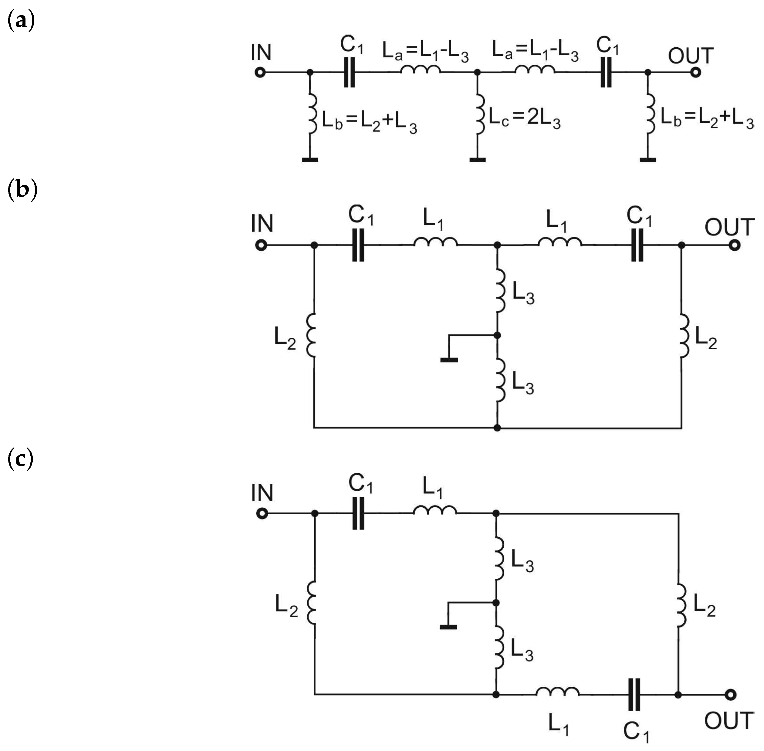
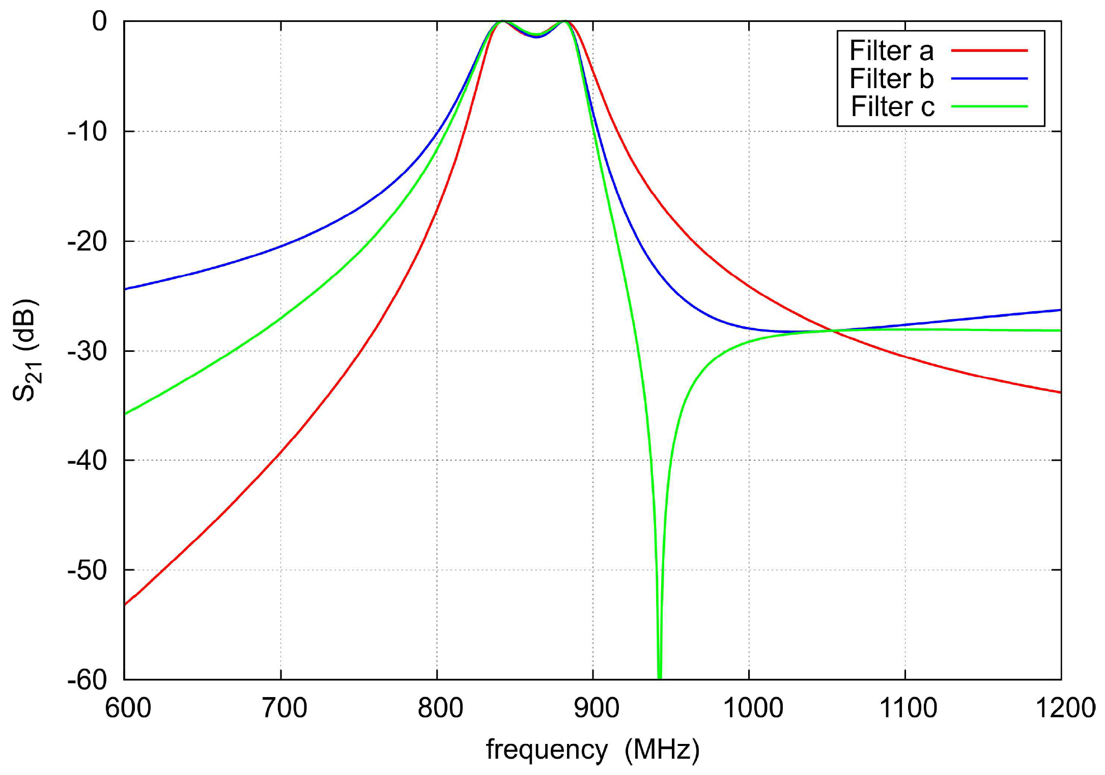
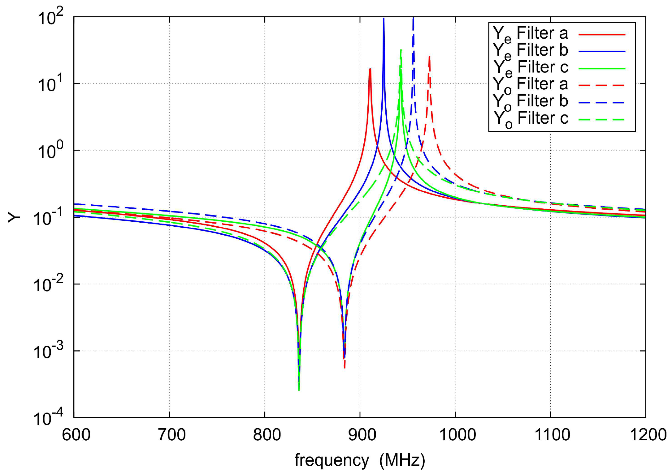
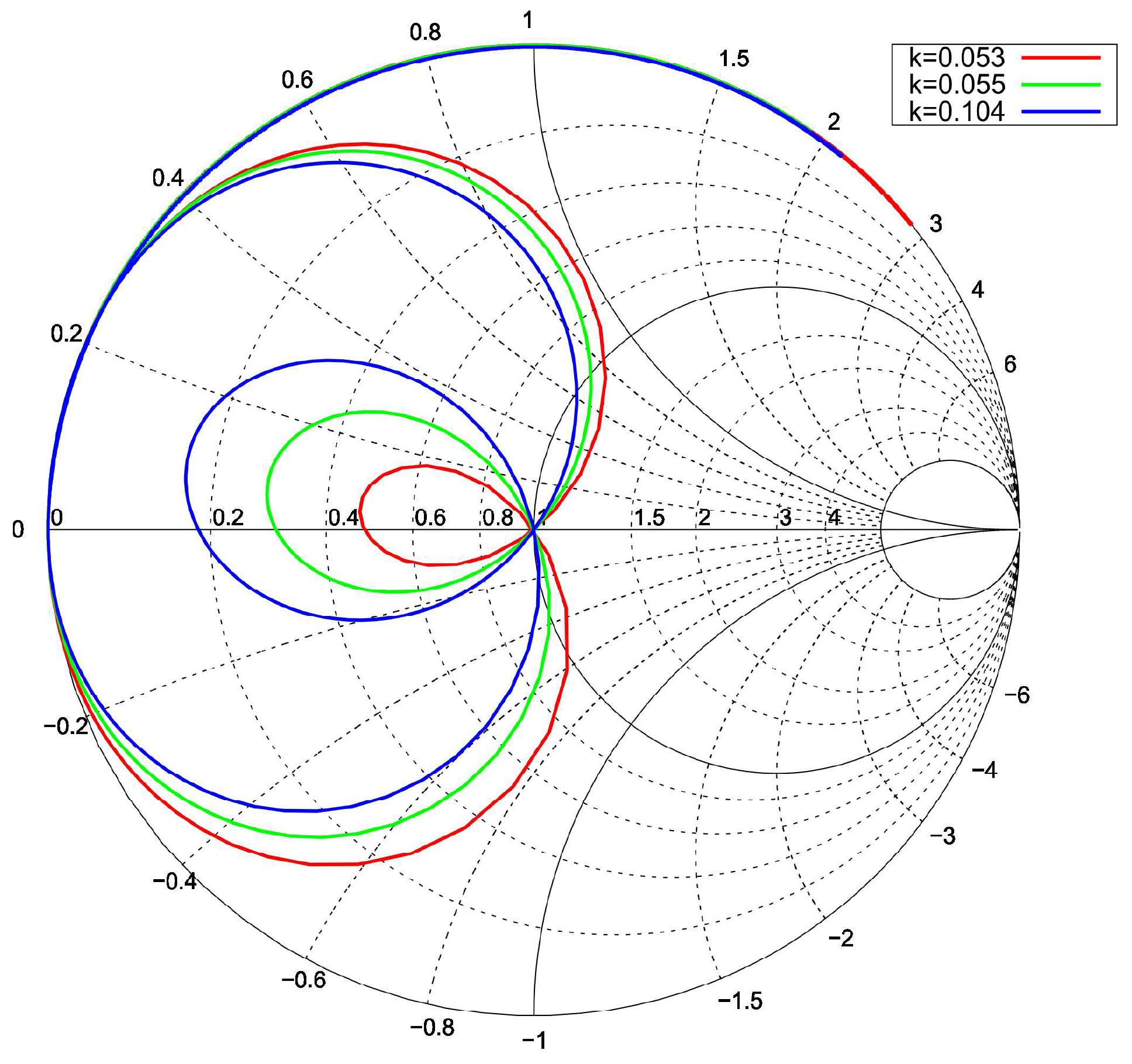
2. Lumped Element Prototype

The initial circuit for the proposed filter is a well-known lumped double-tuned coupled resonator filter with inductive coupling [2,42,43], shown in Figure 1a. The modifications introduced to its network are shown in Figure 1b,c. The inductances L a , L b , L c and L 1 , L 2 , L 3 were set to obtain the same value of the coupling factor k for all three filter versions [43]:
k = 2 L 3 L 1 + L 2 + 2 L 3 .
The filter shown in Figure 1a consists of two parallel resonators built of the capacitors C 1 and inductors L a , L b , L c . The coupling element is inductor L c . In the circuit shown in Figure 1b, the two coupling elements were introduced by splitting the L c into two separate L 3 inductors of equal inductances and grounding the node of their connection. As a result of the filter transformation, the second coupling element L 3 becomes a common part of the input and output circuit. The comparison of the s 21 versus frequency characteristics of the networks from Figure 1a,b shows that the modified circuit response has a lower slope in the lower transition band, but a steeper slope in the upper transition band. This is an advantage of such a filter when applied as a preselector in RF systems with downconversion and the desired channel frequency lower than the image channel frequency. However, the location of the additional coupling element causes decreased attenuation in the stopband for high frequencies due to the ratio of the L 2 and L 3 inductances. This effect was reduced by swapping the branch containing the L 1 and C 1 elements and the branch containing L 3 within the output resonator, which led to the final solution presented in Figure 1c. The branch swapping introduced an additional transmission zero to filter the frequency response, which improved its upper slope steepness.
The frequency properties of the filter from Figure 1c were investigated by means of a modal analysis [41,42].
The odd-mode Y o ( ω ) and even-mode Y e ( ω ) admittances are given by the formulas:
Y e ( ω ) = 1 j ω   ( L 2 + L 3 ) 1 ω ω 1 2 1 ω ω 3 2
Y o ( ω ) = 1 j ω   ( L 2 + L 3 ) 1 ω ω 2 2 1 ω ω 3 2
where:
ω 1 2 = 1 C 1 ( L 1 + L 2 ) ω 2 2 = 1 C 1 ( L 1 + L 2 + 4 L 3 ) ω 3 2 = L 2 + L 3 C 1 L 2 L 3 + L 1 ( L 2 + L 3 )
ω 1 and ω 2 are the angular frequencies of the zeros of Y o and Y e , respectively. These frequencies control the passband and occur close to the s 21 maxima (if there are ripples in the characteristic). The scattering parameter s 11 ( ω ) is described by the formula:
s 11 ( ω ) = ω 2 L 2 + L 3 2 1 ω ω 3 2   Z 0 2 1 ω ω 1 2 ω 2 L 2 + L 3 2 1 ω ω 3 2   +   2 j ω   L 2 + L 3   Z 0 1 ω ω 3 2 1 ω ω 4 2 +   Z 0 2 1 ω ω 1 2 1 ω ω 2 2
and s 21 ( ω ) by:
s 21 ( ω ) = 4 j ω 3 L 3 ( L 2 + L 3 ) C 1 Z 0 1 ω ω 3 2 ω 2 L 2 + L 3 2 1 ω ω 3 2   +   2 j ω   L 2 + L 3   Z 0 1 ω ω 3 2 1 ω ω 4 2 +   Z 0 2 1 ω ω 1 2 1 ω ω 2 2
Angular frequency:
ω 4 2 = 1 C 1 ( L 1 + L 2 + 2 L 3 )
roughly corresponds to the centre frequency of the filter. At angular frequency ω 3 , there is a transmission zero on the right side of the passband near the upper cutoff frequency of the filter. The presence of the transmission zero improves the steepness of the upper transition band. Since ω 4 and ω 3 are the functions of the C 1 capacitances, tuning the centre frequency of the filter results in a concurrent tuning of the transmission zero frequency.
The frequency behaviour of s 21 and the admittances for even- and odd-mode are shown in Figure 2 and Figure 3 for C 1 = 3.15 pF, L 1 = 8.8 nH, L 2 = 1.5 nH, and L 3 = 0.3 nH. As can be seen, because of the same coupling factor value, all filters have practically indistinguishable s 21 characteristics in the passband. The comparison of the Y e and Y o admittance characteristics of the filters shows that the transmission zero is an effect of the equal pole frequencies of these admittances occurring only for the filter from Figure 1c.
The shape of the characteristic of the proposed filter in the passband depends on the coupling coefficient in a very similar way to the classic double-tuned coupled resonator filter from Figure 1a. This allows the use of calculation methods applied for such filters to calculate initial element values of the proposed filter for a given ripple level or bandwidth. Figure 4 shows three exemplary s 21 characteristics of the proposed filter plotted for the following sets of component values and corresponding coupling coefficients:
  • C 1 = 2.85 pF, L 1 = 8.8 nH, L 2 = 2.66 nH, L 3 = 0.34 nH, k = 0.053;
  • C 1 = 3.15 pF, L 1 = 8.8 nH, L 2 = 2.66 nH, L 3 = 0.3 nH, k = 0.055;
  • C 1 = 3 pF, L 1 = 8.8 nH, L 2 = 1.5 nH, L 3 = 0.6 nH, k = 0.104.
As can be seen, for suitably small coupling coefficients, the course of the filter parameter s 21 is devoid of ripples in the passband. An increase in the coupling coefficient causes the bandwidth to widen and the distance from the upper cutoff frequency to the transmission zero frequency to decrease. Exceeding a certain value of the coupling coefficient causes ripples in the s 21 and deterioration of the s 11 parameter (see Figure 5). The limit of the filter response at infinite frequency is given by the formula:
lim f | s 21 | = 2 L 3 L 1 + L 2 + 2 L 3
and it is numerically equal to the coupling coefficient k. Hence, the bandwidth and the achieved out-of-band attenuation are related to each other, and the increase in the coupling coefficient causes the passband to be broadened and deteriorates the attenuation in the stopband.

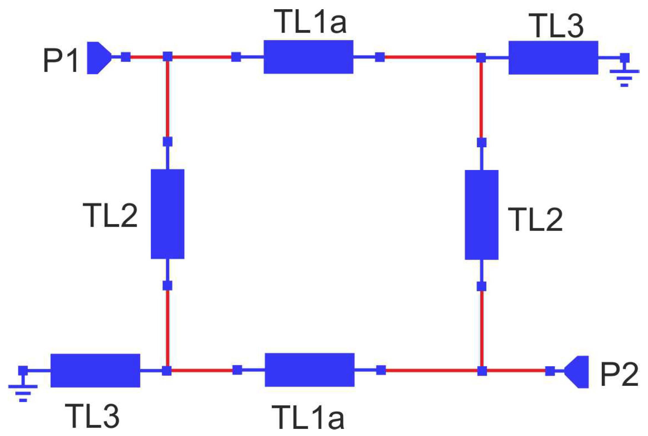
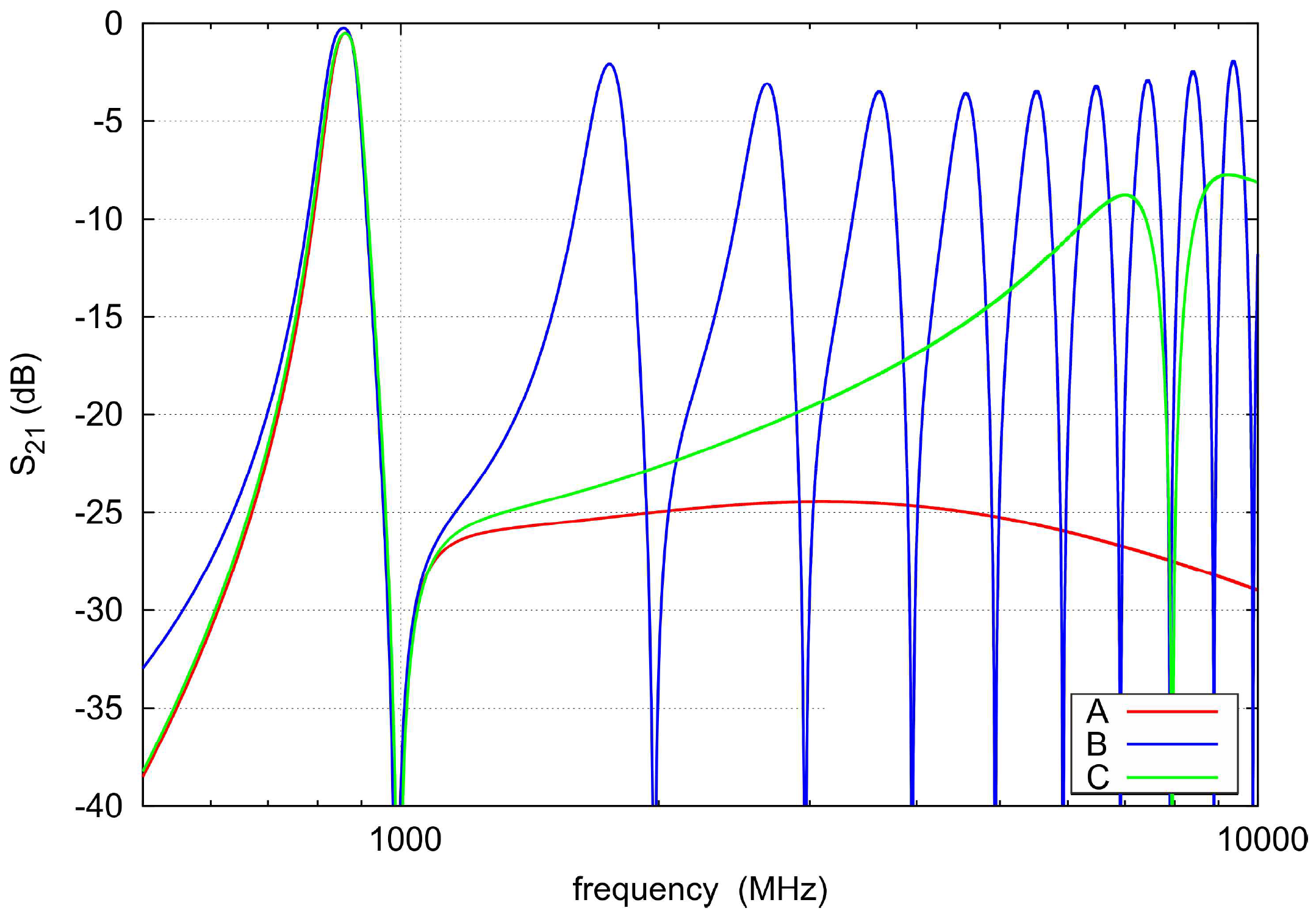
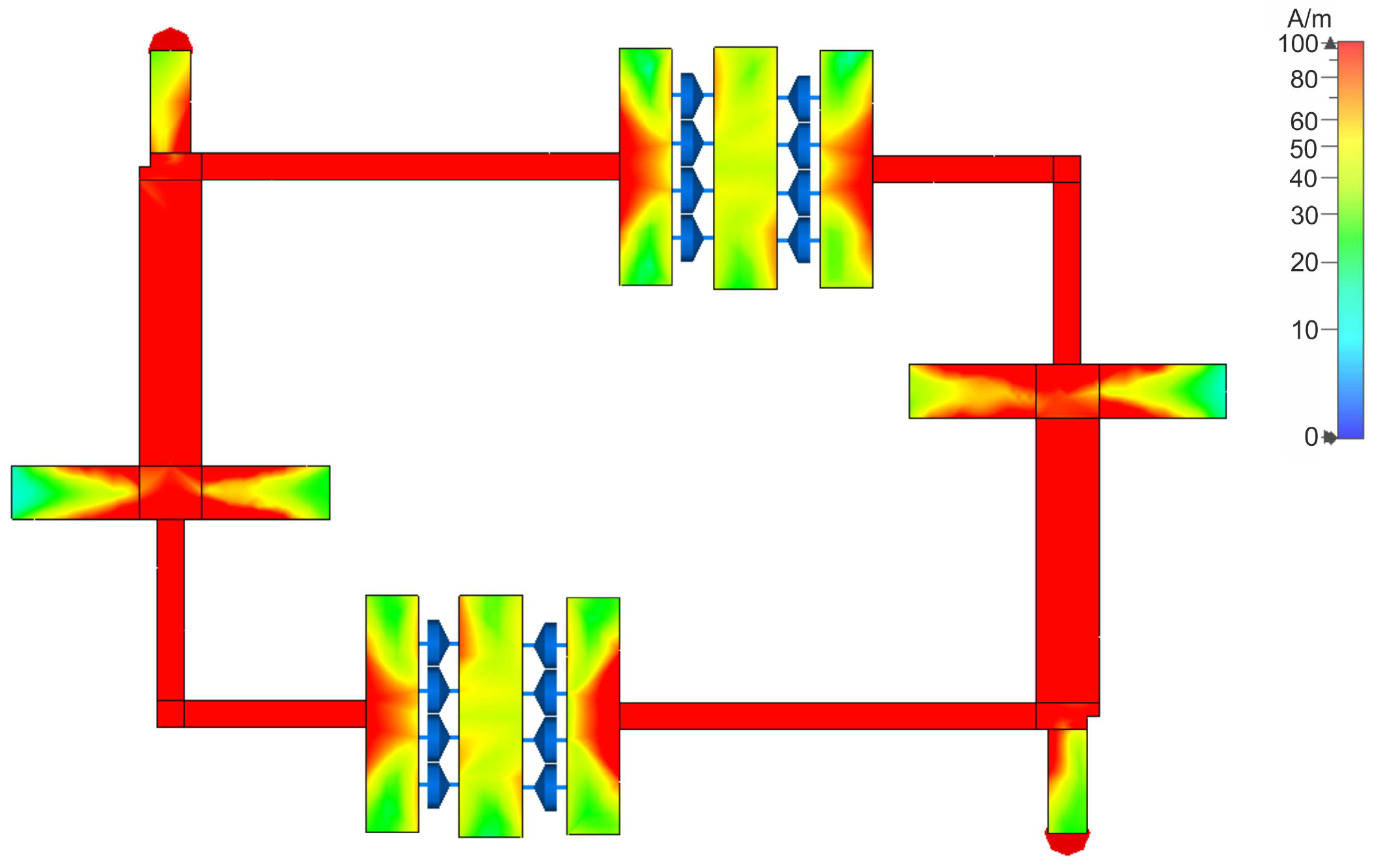
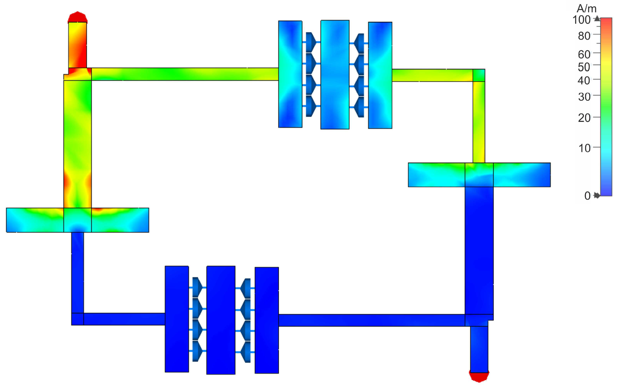
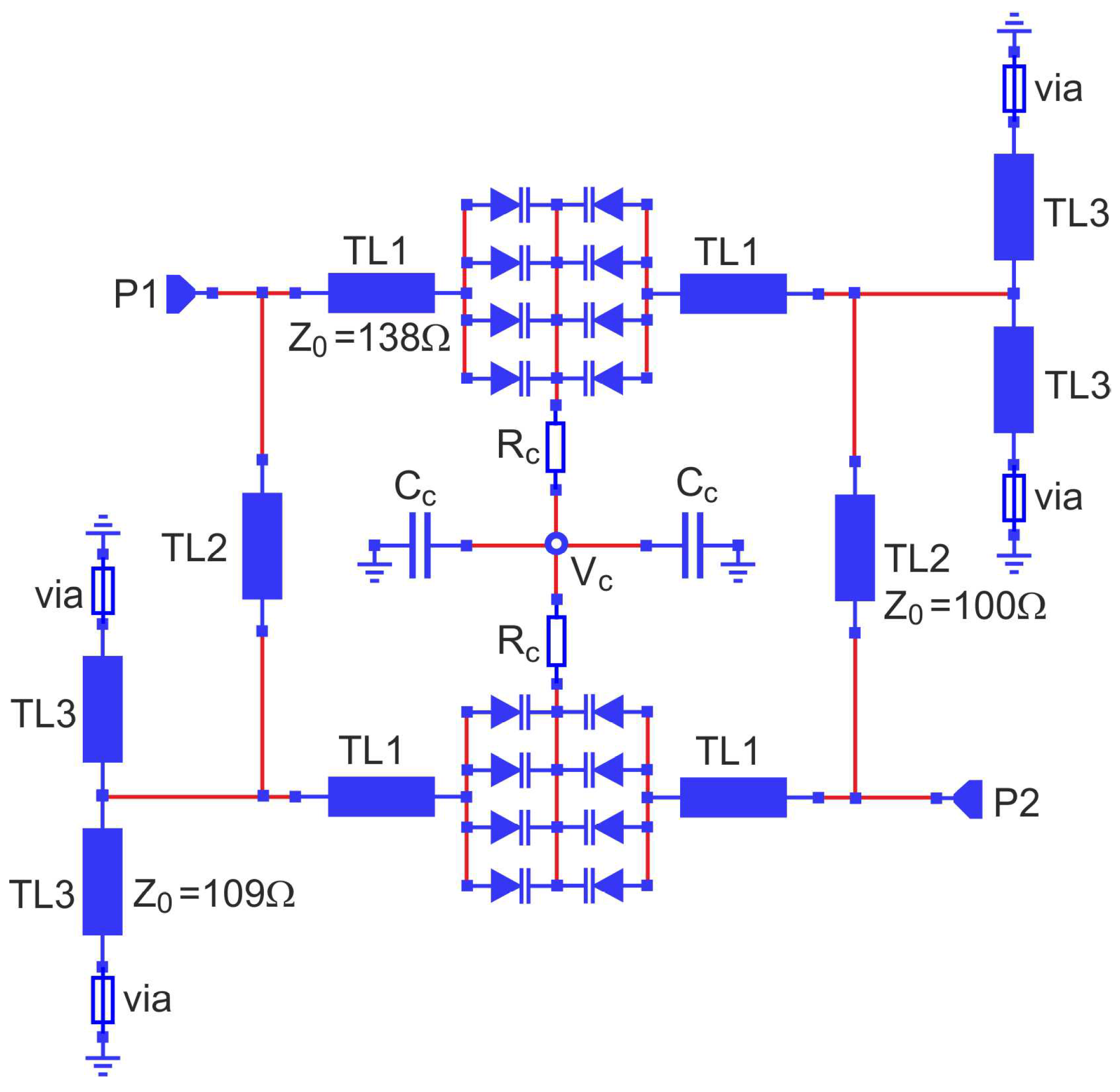
3. Filter with the Implementation of the Transmission Lines
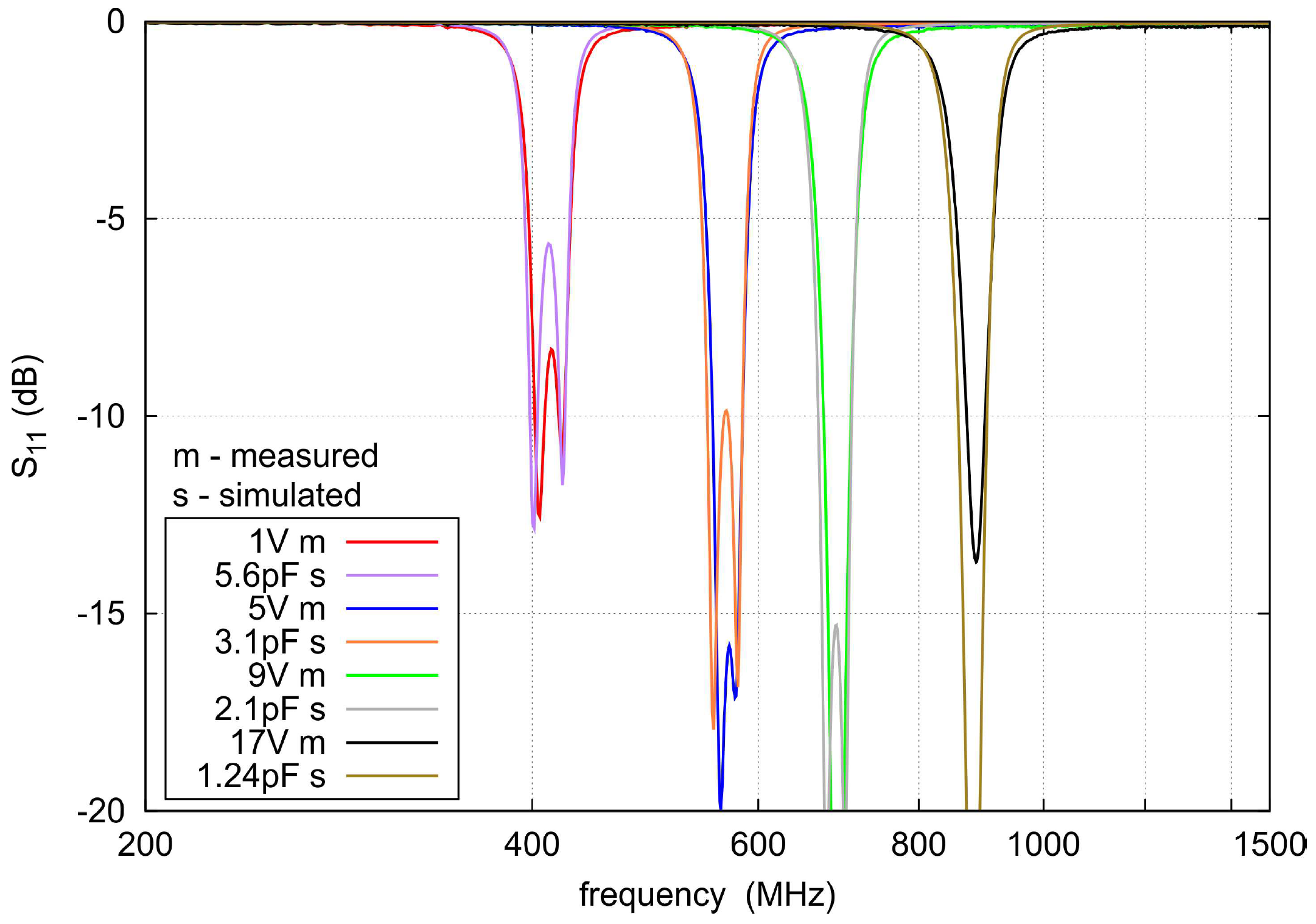
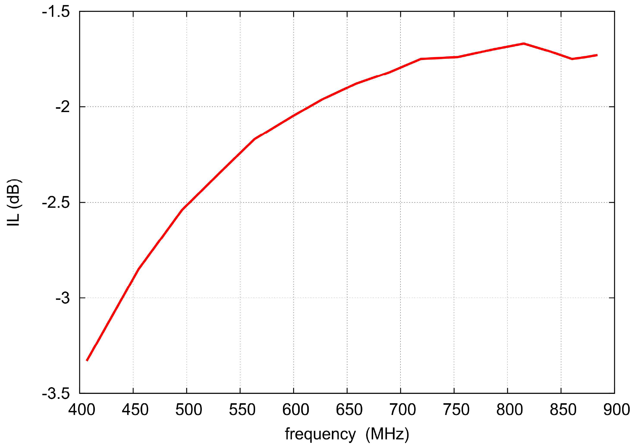
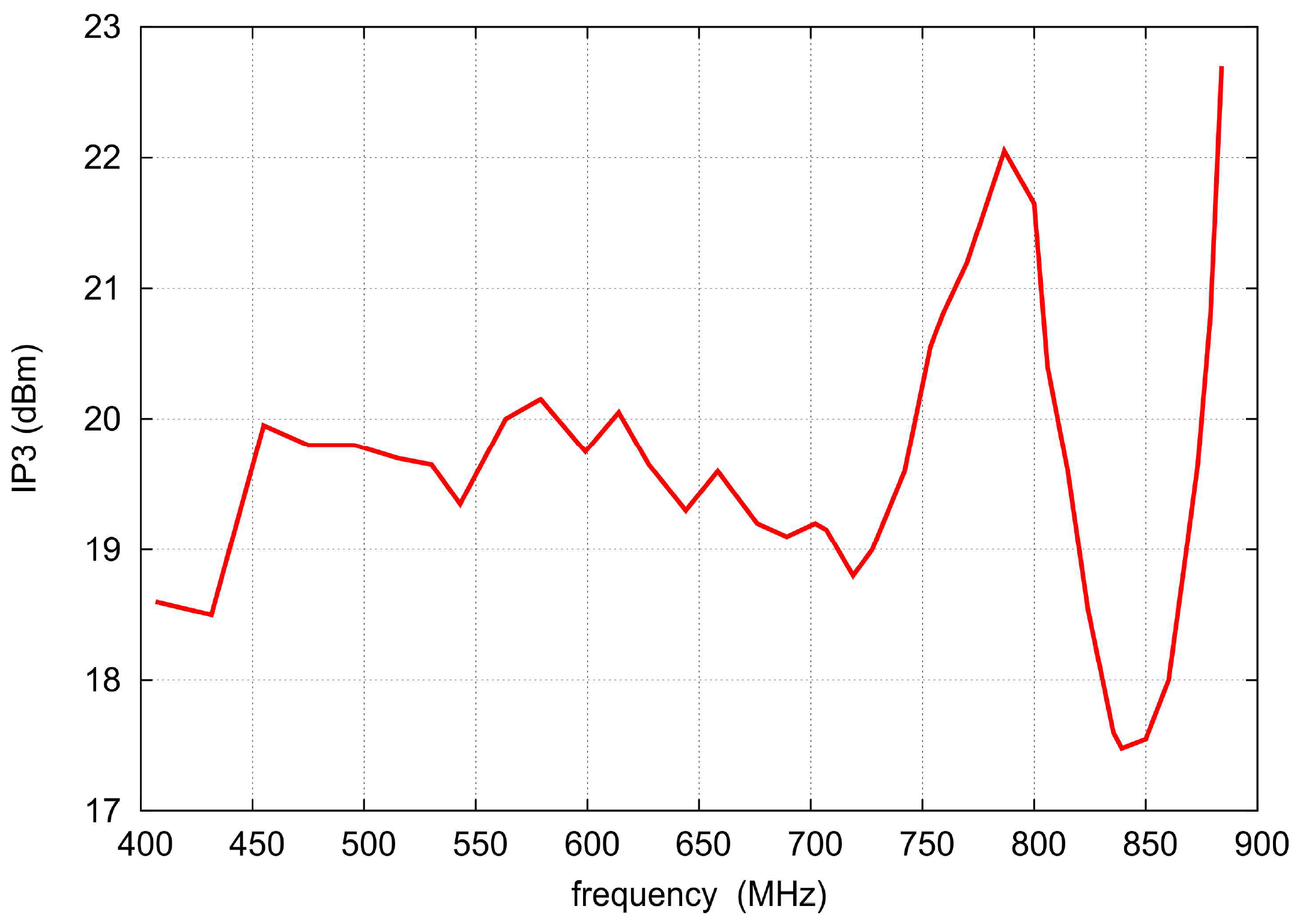
In the microwave frequency range, the filter prototype from Figure 1c can be easily realized with the implementation of the transmission lines by means of the known methods describing lumped and distributed element correspondence.
For the fixed centre frequency realisation, the filter shown in Figure 6 adopts the TL2 and TL3 lines, which are the equivalents of the L 2 and L 3 inductors. The line lengths and characteristic impedances are related to the inductances by the equation:
ω L = Z 0 tan β l β l 1 for f m a x
describing the input reactance of the shorted transmission line. The TL2 and TL3 lines should be electrically shorted for the highest frequency of interest f m a x . The branch consisting of a series connection of L 1 and C 1 is replaced by a TL1a transmission line of characteristic impedance Z 0 and the electrical length of π occurring at the angular frequency ω 0 given by the following equation [41]:
Z 0 = 2 π L 1 C 1 β l = π for ω 0 = 1 L 1 C 1
The frequency response of the filter designed with the application of the transmission lines instead of lumped elements is shown in Figure 7 as Curve B. The parameters of applied lines given in Table 1 were calculated for C 1 = 2.85 pF, L 1 = 8.8 nH, L 2 = 2.66 nH, L 3 = 0.34 nH according to (9) and (10). Curve A in Figure 7 presents the lumped element filter prototype response. The angular frequency ω 0 is located close to the transmission zero frequency, so that the half-wave line properly replaces the L 1 - C 1 branch in the passband, but the lower transition band approximation of the filter response is worse than the upper. Due to the length of the transmission line used instead of the L 1 - C 1 branch, the additional passbands successively appear at frequencies close to the multiples of the centre frequency of the filter.
In the alternative fixed centre frequency version of the filter shown in Figure 8, the capacitors C 1 = 2.85 pF are left at the same positions as in the lumped prototype and the inductors L 1 are replaced by the electrically shorted sections of the TL1b lines. The TL2 and TL3 lines were adopted in the same way as in the realisation shown in Figure 6. To obtain the additional parasitic passband far from the operating band, the electrical length of the line TL1b should be small; therefore, its characteristic impedance should be assumed as high as can be practically achieved. Curve C in Figure 7 shows the exemplary s 21 frequency behaviour for the TL1b characteristic impedance Z 0 = 140 Ω and the electrical length equal to 9.38 deg at 860 MHz. Thanks to the application of the high Z 0 impedance, the centre frequency of the additional band is 7 GHz. However, the location of this band likely appears at a lower frequency in practice due to the physical layout of the filter and its dimensions.

4. Tunable Filter

The filter shown in Figure 8 can be realised as a tunable network by replacing the capacitors C 1 with varactors controlled by a common voltage. In the following example, the filter tuning range from 430 MHz to 860 MHz was assumed. A 1SV280 varactor diode of capacitance tuning range from 1.2 pF to 5.5 pF for 1 V to 17 V of control voltage swing was chosen. Therefore, obtaining the assumed frequency tuning range of the designed filter required the use of two 1SV280 varactors connected in parallel. In order to improve the linearity of the filter, it was decided to use a push–pull connection of eight varactors instead of each C 1 capacitor, as shown in Figure 9. The series resistance of the chosen varactor varied from 0.2 Ω to 0.44 Ω . The result of the varactors’ connection was a two-fold reduction of the equivalent series resistance and a decrement of filter insertion loss.
The filter was designed and fabricated on a Rogers 5870 substrate of thickness h = 1.5 mm and ε r = 2.33. Due to the low value of the inductances L 3 , they were realised as a parallel connection of two identical elements consisting of the transmission line TL3 grounded by a via of estimated inductance of 0.4 nH. The bias network elements R c and C c were added to the varactors network.
In Figure 10, the layout of the tunable filter is presented. The dimensions of the layout were 22 × 15 mm (excluding connectors). Thanks to the filter-specific topology, the layout had a compact structure and small dimensions. Additionally, its consistency was improved by placing the varactor bias network at the spare place in the centre of the structure. The photo of the filter prototype assembled by the authors is depicted in Figure 11.
The scattering parameters of the prototype were measured with the Agilent N5230A network analyser for the tuning voltage swing from 1 V to 17 V. For the layout shown in Figure 10, the full-wave simulations were performed via the CST Microwave Studio software using a frequency-domain simulator. The varactors were modelled as the lumped capacitors with series resistances. The varactors’ capacitances were adjusted during the simulations to obtain convergence with the measurements results.
The results of the measurements and full-wave simulations are compared in Figure 12 and Figure 13. The agreement was very good. The obtained filter tuning range was from 410 MHz to 880 MHz, which was wider than was initially assumed. The reflection coefficient within the tuning range was better than −9 dB; the insertion loss varied monotonically from 3.37 dB to 1.7 dB (see Figure 14); the fractional bandwidth was from 7.5% to 8%. Transmission zero attenuation of 50 dB was constant during the filter tuning. The transmission zero frequency to the centre frequency ratio was about 1.17. The shape factor of the proposed filter, which is defined as the ratio of the bandwidth for 3 dB attenuation to the bandwidth for 30 dB attenuation, varied from 0.2 to 0.18.
The broadband filter responses measured for the various control voltages are presented in Figure 15. The additional bandpass occurred at 3.5 GHz. It is noticeable that the out-of-band behaviour of s 21 was determined only by the filter topology and practically independent of the control voltage. This distinguishes the proposed filter from the majority of filters described in the literature, and it is convenient to eliminate this band by the use of a lowpass filter.
Figure 16, Figure 17 and Figure 18 show the simulated current density distributions for the proposed filter tuned to the centre frequency of 566 MHz. The simulations were performed with the omission of a bias network. The current distribution at the centre frequency is shown in Figure 16, in Figure 17 at the transmission zero frequency of 665 MHz, and in Figure 18 in the stopband at a frequency of 1000 MHz. In the operating band, the current density was uniform within both resonators. In contrast, for the transmission zero frequency, the current flow was observed mainly through the TL1 of the resonator located on the input side, shorting the signal to the ground. The current density within the TL2 line of the input resonator and the TL3 line was significantly lower. The resonator on the output side was very weakly excited. In the stopband, the greatest current density was observed within lines TL1 and TL2 on the input side and TL3. The resonator on the output side was practically not excited. The comparison of the current distribution from Figure 17 and Figure 18 shows that the higher attenuation obtained at the transmission zero frequency was an effect of the compensation of the currents within the TL1 and TL2 branches of the output resonator.
The IP3 of the fabricated prototype filter was measured with two HP 8665B signal generators, a directional combiner, and an R&S FSV30 spectrum analyser. The measurement was performed with a two-tone offset of 1 MHz and a signal level of −14.5 dBm (at the combiner output). The results are presented in Figure 19. The IP3 varied from 17.5 to 22.7 dBm.
Table 2 presents a comparison of the proposed filter to the bandpass tunable microstrip filters with a constant fractional bandwidth reported in the literature. The parameters of the tuning range factor ( f max / f min ), insertion loss, fractional bandwidth, IP3, the number of control voltages, the number of resonators, the normalized upper transition bandwidth T B n , and electrical size were compared. The electrical size of the filters is expressed in the guided wavelength ( λ g ) at the lowest operating frequency. T B n was defined by the authors as:
T B n = f 20 dB f 3 dB f 0
where f 0 is the centre frequency of the filter, f 3 dB is the frequency for which s 21 has a relative level −3 dB in the upper transition band, and f 20 dB is the frequency for which s 21 has a relative level of −20 dB in the upper transition band.
The proposed filter offered the broadest tuning range f m a x / f m i n = 2.15 ; the following filter [6] had f m a x / f m i n = 2.05 . The insertion loss varied from 1.7 dB to 3.3 dB, which was the third result after [8,9], having a maximal IL of 2.8 dB and 2.9 dB, respectively. The variation of the relative BW was similar to the other filters. The IP3 of the proposed filter varied from 17.5 dBm to 22.7 dBm. In [10], the IP3 varied from 16 dBm to 22 dBm; in [11], the IP3 varied from 8 dBm to 30 dBm. The IP3 for the other reference filters was not presented by the authors. The proposed filter offered the highest minimum IP3 value within the whole tuning range. Despite the low order, the filter had a steep slope at the upper transition band due to the transmission zero tuned simultaneously with the centre frequency. The filters described in [7,10,11], which presented greater steepness in the upper transition band, had a larger number of resonators than the presented one. The clear advantages of the proposed filter over the reference filters are its very small size, simple structure, and convenient tuning performed with only the control voltage. The small size allows the miniaturization of devices and enables the reduction of the materials’ cost. The simple layout and standard via connection facilitate fabrication and minimize production costs. The single control voltage minimizes the complexity of the tuning circuitry.

5. Conclusions

A tunable filter, controlled by a single voltage, having a compact structure and a narrow upper transition region obtained by an additional transmission zero, was presented. The lumped elements prototype filter was discussed with the addition of the equations describing its parameters. The practical implementation of the microstrip version of the filter tuned by the varactors in the frequency range from 410 MHz to 880 MHz was shown. The filter properties were experimentally verified and compared to other designs. The obtained filter parameters make it useful as an element of preselector networks working in the RF systems where the image channel occurs at a higher frequency than the desired channel. The very small size of the proposed filter encourages the use of a couple of cascaded networks in a preselector design to increase the stopband attenuation and the transition regions’ steepness.

Author Contributions

Conceptualization, M.M. and D.W.; methodology, D.W. and M.S.; validation, M.S., M.M. and A.N.; formal analysis, D.W. and M.M.; investigation, A.N. and M.S.; resources, M.S. and M.M.; data curation, A.N. and M.S.; writing—original draft preparation, D.W. and A.N.; writing—review and editing, M.M. and A.N.; visualization, A.N.; supervision, D.W. All authors have read and agreed to the published version of the manuscript.

Funding

The results presented in this contribution were the outcome of the statutory activities of the Department of Electronics, Electrical Engineering and Microelectronics of Silesian University of Technology financed by the Polish Ministry of Science and Higher Education.

Conflicts of Interest

The authors declare no conflict of interest.

Abbreviations

The following abbreviations are used in this manuscript:
BPFBandpass filter
BWBandwidth
CABWConstant absolute bandwidth
CFBWConstant fractional bandwidth
ILInsertion loss
IP3Third-order intercept point
MEMSMicroelectromechanical system
NCVNumber of control voltages
NRNumber of resonators
RFRadio frequency
YIGYttrium iron garnet

References

  1. Carr, J.J. Technician’s Radio Receiver Handbook: Wireless and Telecommunication Technology, 1st ed.; Newnes: Oxford, UK, 2001. [Google Scholar]
  2. Matthaei, G.L.; Young, L.; Jones, E.M.T. Microwave Filters, Impedance-Matching Networks, and Coupling Structures, 1st ed.; Artech House: Norwood, MA, USA, 1980. [Google Scholar]
  3. Du, T.; Guan, B.; Zhang, P.; Gu, Y.; Wei, D. An intrinsically switched tunable CABW/CFBW bandpass filter. Electronics 2021, 10, 1318. [Google Scholar] [CrossRef]
  4. Chen, C.-F.; Wang, G.-Y.; Li, J.-J. Microstrip switchable and fully tunable bandpass filter with continuous frequency tuning range. IEEE Microw. Wirel. Compon. Lett. 2018, 28, 500–502. [Google Scholar] [CrossRef]
  5. El-Tanani, M.A.; Rebeiz, G.M. Corrugated microstrip coupled lines for constant absolute bandwidth tunable filters. IEEE Trans. Microw. Theory Tech. 2010, 58, 956–963. [Google Scholar] [CrossRef]
  6. Zhang, G.; Xu, Y.; Wang, X. Compact tunable bandpass filter with wide tuning range of centre frequency and bandwidth using short coupled lines. IEEE Access 2018, 6, 2962–2969. [Google Scholar] [CrossRef]
  7. Li, C.; Bian, Y.; Li, G.; Wu, Y.; Wang, J.; Wang, X.; Zhang, X.; Xia, F.; Bai, D.; Sun, L.; et al. A tunable high temperature superconducting bandpass filter realized using semiconductor varactors. IEEE Trans. Appl. Supercond. 2014, 24, 1–5. [Google Scholar]
  8. Qin, W.; Cai, J.; Li, Y.-L.; Chen, J.-X. Wideband tunable bandpass filter using optimized varactor-loaded SIRs. IEEE Microw. Wirel. Compon. Lett. 2017, 27, 812–814. [Google Scholar] [CrossRef]
  9. Tang, C.-W.; Tseng, C.-T.; Chang, S.-C. A tunable bandpass filter with modified parallel-coupled Line. IEEE Microw. Wirel. Compon. Lett. 2013, 23, 190–192. [Google Scholar] [CrossRef]
  10. Zakharov, A.; Rozenko, S.; Ilchenko, M. Varactor-tuned microstrip bandpass filter with loop hairpin and combline resonators. IEEE Trans. Circuits Syst. II Exp. Briefs 2019, 66, 953–957. [Google Scholar] [CrossRef]
  11. Gao, L.; Rebeiz, G.M. A 0.97–1.53-GHz tunable four-pole bandpass filter with four transmission zeroes. IEEE Microw. Wirel. Compon. Lett. 2019, 29, 195–197. [Google Scholar] [CrossRef]
  12. Lalbakhsh, A.; Ghaderi, A.; Mohyuddin, W.; Simorangkir, R.B.V.B.; Bayat-Makou, N.; Ahmad, M.S.; Lee, G.H.; Kim, K.W.D. A compact C-band bandpass filter with an adjustable dual-band suitable for satellite communication systems. Electronics 2020, 9, 1088. [Google Scholar] [CrossRef]
  13. Kim, I.K.; Kingsley, N.; Morton, M.; Bairavasubramanian, R.; Papapolymerou, J.; Tentzeris, M.M.; Yook, J.-G. Fractal-shaped microstrip coupled-line bandpass filters for suppression of second harmonic. IEEE Trans. Microw. Theory Tech. 2005, 53, 2943–2948. [Google Scholar]
  14. Lalbakhsh, A.; Lotfi Neyestanak, A.A.; Naser-Moghaddasi, M. Microstrip Hairpin bandpas filter using modified Minkowski fractal-shape for suppression of second harmonic. IEICE Trans. Electron. 2012, E95-C, 378–381. [Google Scholar] [CrossRef]
  15. Shen, G.; Che, W.; Feng, W.; Wang, C. Realization of multiple transmission zeroes for bandpass filters with simple inline topology. IEEE Trans. Circuits Syst. II Exp. Briefs 2020, 67, 1029–1033. [Google Scholar] [CrossRef]
  16. Mutalib, M.A.; Zakaria, Z.; Shairi, N.A. Electronically tunable transmission zeros bandpass filter with notch response. In Proceedings of the 18th International Symposium on Antenna Technology and Applied Electromagnetics (ANTEM), Waterloo, ON, Canada, 19–22 August 2018; pp. 1–3. [Google Scholar]
  17. Lalbakhsh, A.; Ghaderi, A.; Mohyuddin, W.; Simorangkir, R.B.V.B.; Bayat-Makou, N.; Ahmad, M.S.; Lee, G.H.; Kim, K.W.D. A compact lowpass filter for satellite communication systems based on transfer function analysis. Int. J. Electron. Commun. 2020, 124, 1–7. [Google Scholar] [CrossRef]
  18. Karimi, G.; Lalbakhsh, A.; Dehghani, K.; Siahkamari, H. Analysis of novel approach to design of ultra-wide stopband microstrip low-pass filter using modified U-shaped resonator. ETRI J. 2015, 37, 945–950. [Google Scholar] [CrossRef]
  19. Simpson, D.J.; Gomez-Garcia, R.; Psychogiou, D. Single-/multi-band bandpass filters and duplexers with fully reconfigurable transfer-function characteristics. IEEE Trans. Microw. Theory Tech. 2019, 67, 1854–1869. [Google Scholar] [CrossRef]
  20. Sanchez-Renedo, M. High-selectivity tunable planar combline filter with source/load-multiresonator coupling. IEEE Microw. Wirel. Compon. Lett. 2007, 17, 513–515. [Google Scholar] [CrossRef]
  21. Song, K.; Chen, W.; Patience, S.R.; Chen, Y.; Iman, A.M.; Fan, Y. Compact wide-frequency tunable filter with switchable bandpass and bandstop frequency response. IEEE Access 2019, 7, 47503–47508. [Google Scholar] [CrossRef]
  22. Saeedi, S.; Lee, J.; Sigmarsson, H.H. Tunable, high-Q, substrate-integrated, evanescent-mode cavity bandpass-bandstop filter cascade. IEEE Microw. Wirel. Compon. Lett. 2016, 26, 240–242. [Google Scholar] [CrossRef]
  23. Psychogiou, D.; Gomez-Garcia, R.; Peroulis, D. Wide-passband filters with in-band tunable notches for agile multi-interference suppression in broad-band antenna systems. In Proceedings of the IEEE Radio and Wireless Symposium (RWS), Anaheim, CA, USA, 15–18 January 2018; pp. 213–216. [Google Scholar]
  24. Lee, T.-C.; Lee, J.; Peroulis, D. Dynamic bandpass filter shape and interference cancellation control utilizing bandpass–bandstop filter cascade. IEEE Trans. Microw. Theory Tech. 2015, 63, 2526–2539. [Google Scholar] [CrossRef]
  25. Islam, H.; Das, S.; Bose, T.; Ali, T. Diode based reconfigurable microwave filters for cognitive radio applications: A review. IEEE Access 2020, 8, 185429–185444. [Google Scholar] [CrossRef]
  26. Jung, M.; Min, B.-W. A widely tunable compact bandpass filter based on a switched varactor-tuned resonator. IEEE Access 2019, 7, 95178–95185. [Google Scholar] [CrossRef]
  27. Luo, X.; Sun, S.; Staszewski, R.B. Tunable bandpass filter with two adjustable transmission poles and compensable coupling. IEEE Trans. Microw. Theory Tech. 2014, 62, 2003–2013. [Google Scholar] [CrossRef] [Green Version]
  28. Zhang, S.-X.; Chen, Z.-H.; Chu, Q.-X. Compact tunable balanced bandpass filter with novel multi-mode resonator. IEEE Microw. Wirel. Compon. Lett. 2017, 27, 43–45. [Google Scholar] [CrossRef]
  29. Brown, A.R.; Rebeiz, G.M. A varactor-tuned RF filter. IEEE Trans. Microw. Theory Tech. 2000, 48, 1157–1160. [Google Scholar] [CrossRef]
  30. Abbaspour-Tamijani, A.; Dussopt, L.; Rebeiz, G.M. Miniature and tunable filters using MEMS capacitors. IEEE Trans. Microw. Theory Tech. 2003, 51, 1878–1885. [Google Scholar] [CrossRef]
  31. Mao, J.; Che, W.; Ma, Y.; Chen, J. Tunable differential-mode bandpass filters with wide tuning range and high common-mode suppression. IET Microw. Antennas Propag. 2014, 8, 437–444. [Google Scholar] [CrossRef]
  32. Chiou, Y.-C.; Rebeiz, G.M. A quasi elliptic function 1.75–2.25 GHz 3-pole bandpass filter with bandwidth control. IEEE Trans. Microw. Theory Tech. 2012, 60, 244–249. [Google Scholar] [CrossRef]
  33. Kingsly, S.; Kanagasabai, M.; Mohammed, G.N.A.; Subbaraj, S.; Selvam, Y.P.; Natarajan, R. Multi-band reconfigurable microwave filter using dual concentric resonators. Int. J. RF Microw. Comput. Aided. Eng. 2018, 28, e21290. [Google Scholar] [CrossRef]
  34. Zhang, N.; Mei, L.; Wang, C.; Deng, Z.; Yang, J.; Guo, Q. A switchable bandpass filter employing RF MEMS switches and open-ring resonators. IEEE Trans. Electron Devices 2017, 64, 3377–3383. [Google Scholar] [CrossRef]
  35. Ebrahimi, A.; Baum, T.; Scott, J.; Ghorbani, K. Continuously Tunable Dual-Mode Bandstop Filter. IEEE Microw. Wirel. Compon. Lett. 2018, 28, 419–421. [Google Scholar] [CrossRef] [Green Version]
  36. Zhang, R.; Gomez-Garcia, R.; Peroulis, D. Multifunctional bandpass filters with reconfigurable and switchable band control. IEEE Trans. Microw. Theory Tech. 2019, 67, 2355–2369. [Google Scholar] [CrossRef]
  37. Tsai, H.-J.; Huang, B.-C.; Chen, N.-W.; Jeng, S.-K. A reconfigurable bandpass filter based on a varactor-perturbed, T-shaped dual-mode resonator. IEEE Microw. Wirel. Compon. Lett. 2014, 24, 297–299. [Google Scholar] [CrossRef]
  38. Cho, Y.-H.; Park, C.; Yun, S.-W. 0.7–1.0-GHz switchable dual-/single-band tunable bandpass filter using a switchable J-inverter. IEEE Access 2021, 9, 16967–16974. [Google Scholar] [CrossRef]
  39. Xiang, Q.; Feng, Q.; Huang, X. Electrical tunable microstrip LC bandpass filters with constant bandwidth. IEEE Trans. Microw. Theory Tech. 2013, 61, 1124–1130. [Google Scholar] [CrossRef]
  40. Tsai, C.S.; Qiu, G. Wideband microwave filters using ferromagnetic resonance tuning in flip-chip YIG-GaAs layer structures. IEEE Trans. Magn. 2009, 45, 656–660. [Google Scholar] [CrossRef]
  41. Pozar, D.M. Microwave Engineering, 3rd ed.; John Wiley & Sons: Hoboken, NJ, USA, 2005. [Google Scholar]
  42. Hong, J.-S.; Lancaster, M.J. Microstrip Filters for RF Microwave Applications; John Wiley & Sons: Hoboken, NJ, USA, 2001. [Google Scholar]
  43. Dishal, M. Design of dissipative band-pass filters producing desired exact amplitude-frequency characteristics. Proc. IRE 1949, 37, 1050–1069. [Google Scholar] [CrossRef]
Figure 1. Lumped element bandpass filters: (a) the initial circuit of the double-tuned coupled resonator filter, (b) the filter with a split coupling inductance, and (c) the filter with swapped branches within the output resonator.
Electronics 10 02315 g001
Figure 2. Frequency behaviour of s 21 of the double-tuned coupled resonator filter versions presented in Figure 1.
Electronics 10 02315 g002
Figure 3. Frequency behaviour of the Y e and Y o admittances of the double-tuned coupled resonator filter versions presented in Figure 1.
Electronics 10 02315 g003
Figure 4. Exemplary s 21 characteristics of the proposed filter for three values of the coupling coefficient: k = 0.053 ( C 1 = 2.85 pF, L 1 = 8.8 nH, L 2 = 2.66 nH, L 3 = 0.34 nH), k = 0.055 ( C 1 = 3.15 pF, L 1 = 8.8 nH, L 2 = 2.66 nH, L 3 = 0.3 nH), k = 0.104 ( C 1 = 3 pF, L 1 = 8.8 nH, L 2 = 1.5 nH, L 3 = 0.6 nH).
Electronics 10 02315 g004
Figure 5. Exemplary s 11 characteristics of the proposed filter for three values of coupling coefficient: k = 0.053 ( C 1 = 2.85 pF, L 1 = 8.8 nH, L 2 = 2.66 nH, L 3 = 0.34 nH), k = 0.055 ( C 1 = 3.15 pF, L 1 = 8.8 nH, L 2 = 2.66 nH, L 3 = 0.3 nH), k = 0.104 ( C 1 = 3 pF, L 1 = 8.8 nH, L 2 = 1.5 nH, L 3 = 0.6 nH).
Electronics 10 02315 g005
Figure 6. The full transmission line implementation of the lumped prototype filter is shown in Figure 1c.
Electronics 10 02315 g006
Figure 7. Comparison of the frequency responses of the lumped element prototype filter (A), full transmission line implementation of the prototype filter (B), and capacitively loaded implementation of the prototype filter (C).
Electronics 10 02315 g007
Figure 8. Capacitively loaded transmission line implementation of the lumped prototype filter shown in Figure 1c.
Electronics 10 02315 g008
Figure 9. Schematic diagram of the proposed tunable bandpass filter.
Electronics 10 02315 g009
Figure 10. Layout of the proposed tunable bandpass filter.
Electronics 10 02315 g010
Figure 11. Photo of the fabricated prototype of the proposed tunable bandpass filter.
Electronics 10 02315 g011
Figure 12. Measured and simulated s 11 of the proposed tunable bandpass filter for the selected control voltages.
Electronics 10 02315 g012
Figure 13. Measured and simulated s 21 of the proposed tunable bandpass filter for the selected control voltages.
Electronics 10 02315 g013
Figure 14. Variation of the insertion loss of the proposed tunable bandpass filter versus frequency.
Electronics 10 02315 g014
Figure 15. s 21 broadband measurements of the proposed tunable bandpass filter for the selected control voltages.
Electronics 10 02315 g015
Figure 16. Exemplary current distribution at the centre frequency (566 MHz) of the filter.
Electronics 10 02315 g016
Figure 17. Exemplary current distribution at the transmission zero frequency (665 MHz) of the filter.
Electronics 10 02315 g017
Figure 18. Exemplary current distribution in the stopband (1000 MHz) of the filter.
Electronics 10 02315 g018
Figure 19. Measured IP3 versus filter centre frequency.
Electronics 10 02315 g019
Table 1. Elements of the filters from Figure 6 and Figure 8.
Element Z 0  ( Ω ) β l  (Deg) f 0  (MHz)
TL1a351801005
TL21008.18860
TL31001.05860
TL1b1409.38860
Table 2. Comparison between the proposed and reference filters.
Ref. f max / f min ILSize ( λ g × λ g )NCVNRCFBW (%)IP3 (dBm) TB n
*2.151.7–3.30.03 × 0.045127.5–8.017.5–22.70.058
[6]2.051.4–4.50.03 × 0.13211.6–15.6-0.18
[7]1.670.8–3.8-142.75–3.2-0.0125
[8]1.691.1–2.80.19 × 0.192215.2–15.9[email protected] GHz0.19
[9]1.522.4–2.90.24 × 0.32226.8–8.4-0.11
[10]1.785.6–9.20.08 × 0.12142.5–2.616–220.018
[11]1.572–4.20.1 × 0.09145.0–6.08–300.042
*—this work, IL—insertion loss, NCV—number of control voltages, NR—number of resonators.
Publisher’s Note: MDPI stays neutral with regard to jurisdictional claims in published maps and institutional affiliations.

