
Optimization of TSV Leakage in Via-Middle TSV Process for Wafer-Level Packaging

Abstract
:1. Introduction
2. Experimental Section
3. Results and Discussion
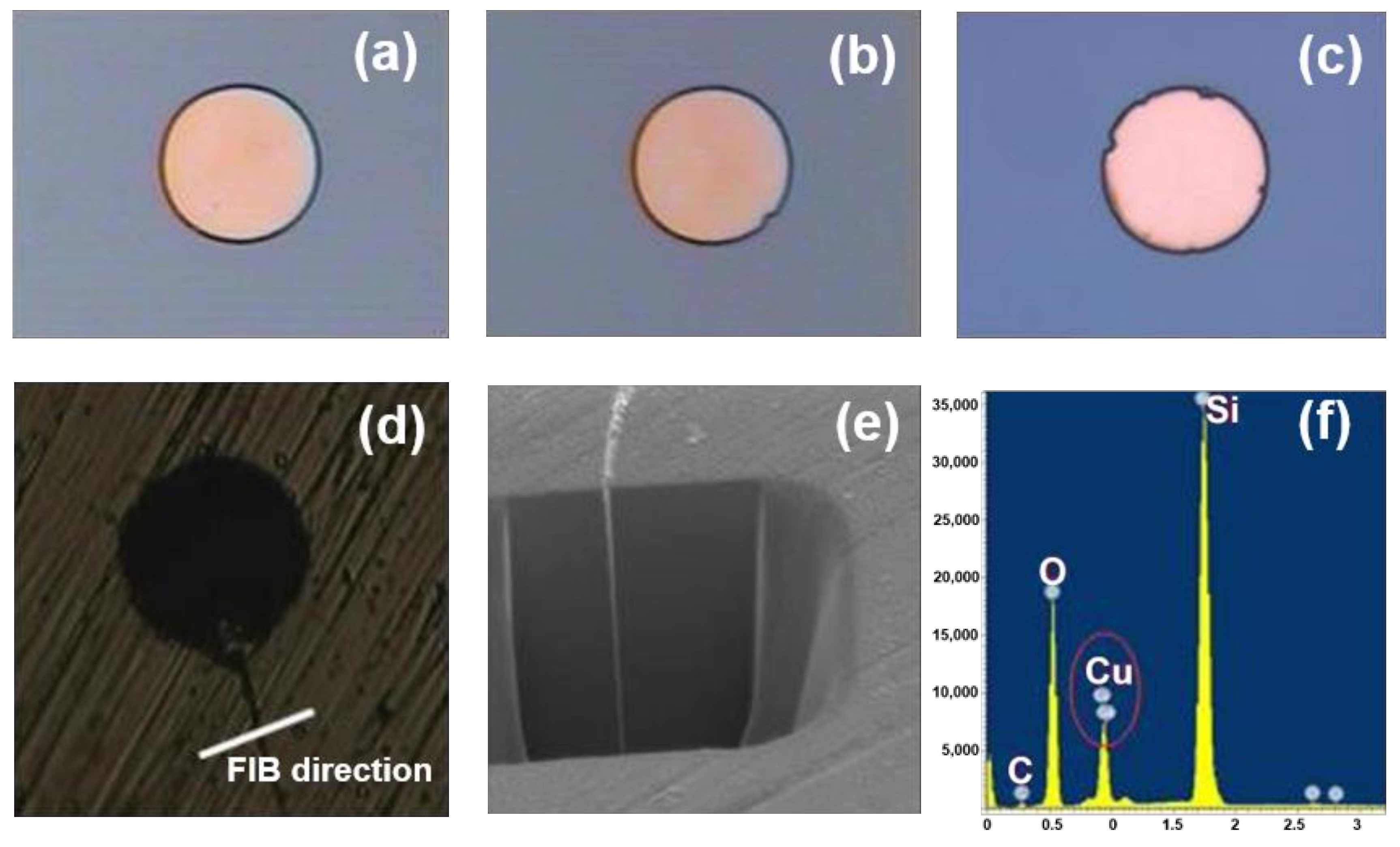
3.1. TSV Leakage Caused by TSV Etch Process
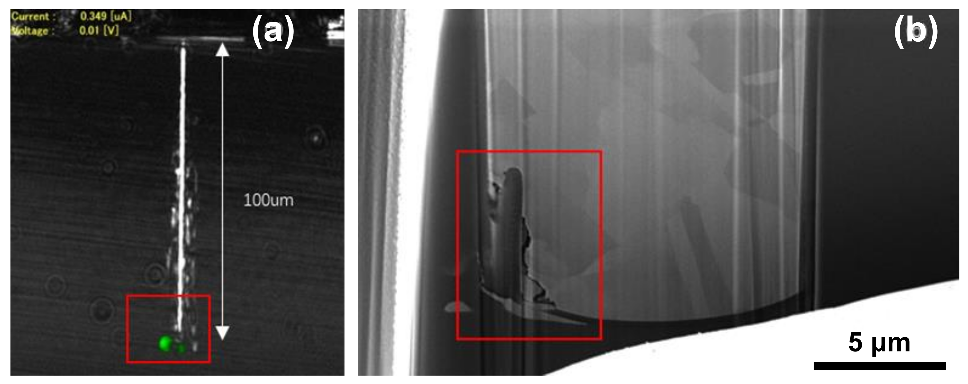
3.2. TSV Leakage Caused by Substrate Bulk Micro Defect (BMD)
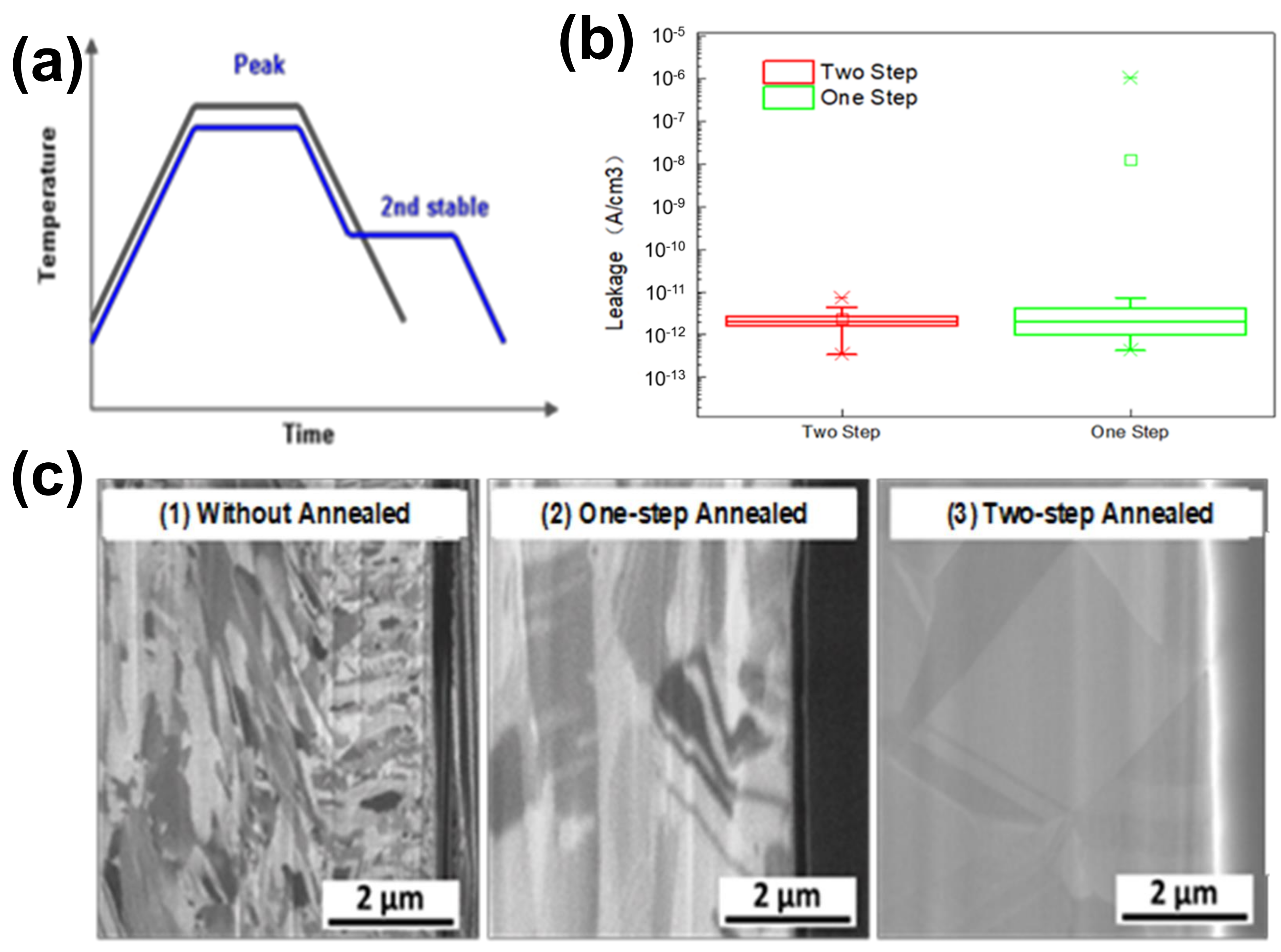
3.3. TSV Leakage Caused by Stress Variation
4. Conclusions
Author Contributions
Funding
Data Availability Statement
Conflicts of Interest
References
- Tan, C.S.; Guttmann, R.J.; Reif, R. Wafer Level 3-D ICs Process Technology; Springer: New York, NY, USA, 2008; pp. 1–11. [Google Scholar]
- Patti, R.S. Three-Dimensional Integrated Circuits and the Future of System-on-Chip Designs. Proc. IEEE 2006, 94, 1214–1224. [Google Scholar] [CrossRef]
- Sadaka, M.; Radu, I.; Di Cioccio, L. 3D integration: Advantages, enabling technologies & applications. In Proceedings of the 2010 IEEE International Conference on Integrated Circuit Design and Technology, Grenoble, France, 2–4 June 2010; pp. 106–109. [Google Scholar] [CrossRef]
- Lee, J.H.; Kim, H.J.; Song, J.-Y.; Lee, C.W.; Ha, T.H. A study on wafer level TSV build-up integration method. In Proceedings of the 2013 IEEE International 3D Systems Integration Conference (3DIC), San Francisco, CA, USA, 2–4 October 2013; pp. 1–4. [Google Scholar] [CrossRef]
- Semiconductor Industry Association. International Technology Roadmap for Semiconductors; Assembly and Packaging: Washington, DC, USA, 2007. [Google Scholar]
- Wang, M.-J.; Hung, C.-Y.; Kao, C.-L.; Lee, P.-N.; Chen, C.-H.; Hung, C.-P.; Tong, H.-M. TSV technology for 2.5D IC solution. In Proceedings of the 2012 IEEE 62nd Electronic Components and Technology Conference, San Diego, CA, USA, 29 May–1 June 2012; pp. 284–288. [Google Scholar] [CrossRef]
- Ren, X.; Xue, K.; Jiang, F.; Wang, Q.; Ping, Y.; Pang, C.; Liu, H.; Xu, C.; Yu, D.; Shangguan, D. Design, simulation, and process development for 2.5D TSV interposer for high performance processer packaging. In Proceedings of the 2013 3rd IEEE CPMT Symposium Japan, Kyoto, Japan, 11–13 November 2013; pp. 1–4. [Google Scholar] [CrossRef]
- Morikawa, Y.; Murayama, T.; Sakuishi, T.; Suzuki, A.; Nakamuta, Y.; Suu, K. Novel TSV process technologies for 2.5D/3D packaging. In Proceedings of the 2014 IEEE 64th Electronic Components and Technology Conference (ECTC), Orlando, FL, USA, 27–30 May 2014; pp. 1697–1699. [Google Scholar]
- Yu, C.L.; Chang, C.H.; Wang, H.Y.; Chang, J.H.; Huang, L.H.; Kuo, C.W.; Tai, S.P.; Hou, S.Y.; Lin, W.L.; Liao, E.B.; et al. TSV process optimization for reduced device impact on 28 nm CMOS. In Proceedings of the 2011 Symposium on VLSI Technology—Digest of Technical Papers, Kyoto, Japan, 14–16 June 2011; pp. 138–139. [Google Scholar]
- Volpert, M.; Soulier, B.; Borel, S.; Ait-Mani, N.; Gaugiran, S.; Gasse, A.; Henry, D. A Wafer Level approach for led packaging using TSV last technology. In Proceedings of the 2015 IEEE 65th Electronic Components and Technology Conference (ECTC), San Diego, CA, USA, 26–29 May 2015; pp. 1102–1108. [Google Scholar] [CrossRef]
- Jing, X.; Dai, F.; Zhang, W.; Cao, L. Via last TSV process for wafer level packaging. In Proceedings of the 2016 17th International Conference on Electronic Packaging Technology (ICEPT), Wuhan, China, 16–19 August 2016; pp. 1216–1218. [Google Scholar] [CrossRef]
- Chui, K.-J.; Li, H.-Y.; Chang, K.-F.; Bhattacharya, S.; Yu, M. A cost model analysis comparing via-middle and via-last TSV processes. In Proceedings of the 2015 IEEE 17th Electronics Packaging and Technology Conference (EPTC), Singapore, 2–4 December 2015; pp. 1–4. [Google Scholar] [CrossRef]
- Katti, G.; Mercha, A.; Stucchi, M.; Tôkei, Z.; Velenis, D.; Van Olmen, J.; Huyghebaert, C.; Jourdain, A.; Rakowski, M.; Debusschere, I.; et al. Temperature dependent electrical characteristics of through-si-via (TSV) interconnections. In Proceedings of the 2010 IEEE International Interconnect Technology Conference, Burlingame, CA, USA, 6–9 June 2010; pp. 1–3. [Google Scholar] [CrossRef]
- Luo, J.; Wang, G.; Sun, Y.; Zhao, X.; Ding, G. Fabrication and characterization of a low-cost interposer with an intact insulation layer and ultra-low TSV leakage current. J. Micromech. Microeng. 2018, 28, 125010. [Google Scholar] [CrossRef]
- Ranganathan, N.; Lee, D.Y.; Youhe, L.; Lo, G.-Q.; Prasad, K.; Pey, K.L. Influence of Bosch Etch Process on Electrical Isolation of TSV Structures. IEEE Trans. Compon. Packag. Manuf. Technol. 2011, 1, 1497–1507. [Google Scholar] [CrossRef]
- Laerme, F.; Schilp, A.; Funk, K.; Offenberg, M. Bosch deep silicon etching: Improving uniformity and etch rate for advanced MEMS applications. In Proceedings of the Technical Digest. IEEE International MEMS 99 Conference. Twelfth IEEE International Conference on Micro Electro Mechanical Systems (Cat. No.99CH36291), Orlando, FL, USA, 21 January 1999; pp. 211–216. [Google Scholar] [CrossRef]
- Kenoyer, L.; Oxford, R.; Moll, A. Optimization of Bosch etch process for through wafer interconnects. In Proceedings of the 15th Biennial University/Government/Industry Microelectronics Symposium (Cat. No.03CH37488), Boise, ID, USA, 2 July 2004; pp. 338–339. [Google Scholar] [CrossRef]
- Zhang, D.; Thangaraju, S.; Smith, D.; Kamineni, H.; Klewer, C.; Scholefield, M.; Lei, M.; Vikram, A.; Lim, V.; Kim, W.; et al. BMD impact on silicon fin defect at TSV bottom. Electron. Lett. 2014, 50, 954–956. [Google Scholar] [CrossRef]


| Condition | Dep. (s) | Clean (s) | Etch (s) | SF6 in Dep. | C4F8 in Clean and Etch |
|---|---|---|---|---|---|
| #1 | T1 | T2 | T3 | L1 | L2 |
| #2 | T1−0.5 | T2−0.2 | T3−0.2 | 2L1 | 2L2 |
| #3 | T1 | T2 | T3−0.4 | 2L1 | 2L2 |
Publisher’s Note: MDPI stays neutral with regard to jurisdictional claims in published maps and institutional affiliations. |
© 2021 by the authors. Licensee MDPI, Basel, Switzerland. This article is an open access article distributed under the terms and conditions of the Creative Commons Attribution (CC BY) license (https://creativecommons.org/licenses/by/4.0/).
Share and Cite
Liu, X.; Sun, Q.; Huang, Y.; Chen, Z.; Liu, G.; Zhang, D.W. Optimization of TSV Leakage in Via-Middle TSV Process for Wafer-Level Packaging. Electronics 2021, 10, 2370. https://doi.org/10.3390/electronics10192370
Liu X, Sun Q, Huang Y, Chen Z, Liu G, Zhang DW. Optimization of TSV Leakage in Via-Middle TSV Process for Wafer-Level Packaging. Electronics. 2021; 10(19):2370. https://doi.org/10.3390/electronics10192370
Chicago/Turabian StyleLiu, Xuanjie, Qingqing Sun, Yiping Huang, Zheng Chen, Guoan Liu, and David Wei Zhang. 2021. "Optimization of TSV Leakage in Via-Middle TSV Process for Wafer-Level Packaging" Electronics 10, no. 19: 2370. https://doi.org/10.3390/electronics10192370
APA StyleLiu, X., Sun, Q., Huang, Y., Chen, Z., Liu, G., & Zhang, D. W. (2021). Optimization of TSV Leakage in Via-Middle TSV Process for Wafer-Level Packaging. Electronics, 10(19), 2370. https://doi.org/10.3390/electronics10192370