Article

A Wide-Band High-Efficiency Hybrid-Feed Antenna Array for mm-Wave Wireless Systems

1
Beijing Institute of Technology, School of Information and Electronic, Beijing 100081, China
2
School of Electronics and Communication Engineering, Sun Yat-sen University, Guangzhou 510275, China
*
Author to whom correspondence should be addressed.
Electronics 2021, 10(19), 2383; https://doi.org/10.3390/electronics10192383
Submission received: 27 August 2021 / Revised: 24 September 2021 / Accepted: 26 September 2021 / Published: 29 September 2021
(This article belongs to the Section Microwave and Wireless Communications)

Abstract

:
A wide-band and high-efficiency planar antenna array with a novel hybrid-feed structure is proposed in this article. By combing the coaxial-line feed magneto-electric (ME) dipoles with the aperture coupled dielectric cavity, a hybrid-feed 2 × 2-unit ME-dipole sub-array is invented. The low-loss ridge gap waveguide (RGWG) corporate-feed network is used to replace the high-loss substrate-based feed networks and high-cost RWG feed networks. New forms of RGWG H-plane divider are designed to build the RGWG feed network. An 8 × 8-unit ME-dipole antenna array is designed and fabricated to verify the validity of the array. The radiation part consists of two layers of a low-cost printed circuit board (PCB), and the feeding part consists of two copper plates manufactured by computer numerical control (CNC) milling. Measured results show that a relative bandwidth of 16.4% with |S11| < −10 dB is achieved, with a maximum radiation efficiency of 85%. The stable symmetric radiation patterns are observed in both the E-plane and H-plane, covering the operation band. Based on the measured results, a 16 × 16-unit ME-dipole antenna array is simulated. Results indicate that the proposed array has wide-band and high-efficiency features, which is suitable for large-scale array design in mm-wave wireless systems.

1. Introduction

Due to the advantages of a high data rate and high detection accuracy, mm-wave wireless systems have been widely used in 5G base stations, auto-motive radar, and blast furnace radar [1,2,3]. A wide-band and high-efficiency mm-wave antenna array is critical to the mm-wave wireless system. In some specific applications, large-scale mm-wave antenna arrays are required to achieve high-gain, narrow beam-width, or multi-direction beams features [3,4,5]. In these applications, both the efficiency, bandwidth, and fabrication cost must be considered in the antenna array design.
The performance of an mm-wave antenna array is determined by the antenna unit and feed network. Various mm-wave planar antenna arrays based on low-cost printed circuit board (PCB) technology have been presented [6,7,8]. The slots array are based on a substrate-integrated waveguide (SIW) in [6,7] and substrate-integrated coaxial line (SICL) in [8]; these arrays have the features of a low-profile and low fabrication cost but suffer from a narrow bandwidth. The ME-dipole is a complementary antenna unit with the advantages of a wide impedance matching band and symmetric radiation patterns [9]. Different kinds of ME-dipoles on the mm-wave band have been reported [10,11,12,13]. These mm-wave arrays exhibit wide-band and low-profile features. However, the feed-networks of these arrays all use the substrate-based transmission line while the substrate loss of the array cannot be ignored with the increase in array dimension.
The slot antenna arrays proposed in [14,15] have waveguide feed networks and the cavity-excited 2 × 2-slot sub-array, which can realize both wide-band and high-efficiency features. However, the high precision diffusion bonding process used in these antenna arrays will bring high fabrication cost. The gap waveguide (GWG) technology [16,17,18] uses an artificial magnetic conductivity (AMC) boundary to build the side-wall of a rectangular waveguide. Based on this technology, a low-loss waveguide transmission line can be fabricated without any expensive bonding process. The mm-wave antenna arrays based on GWG technology [17,18] have a high-gain and reduced fabrication cost but still have the drawbacks of a narrow bandwidth. Some hybrid arrays, by combining low-profile radiation units with GWG or RGWG feed networks, are presented in [19,20,21]. An LTCC-based SIW-feed mixed with an RGWG feed network antenna array is proposed in [20], the array has a wide-band and low-profile but also has a low radiation efficiency. A 1 × 8 CP ME-dipole linear array with a GWG feed network has been reported [21]; it can achieve a relative bandwidth of 13% with |S11| < −10 dB and a gain higher than 18 dBi. However, the feed network occupies too much antenna aperture, which results in a low radiation efficiency. Antenna arrays based on different forms of hybrid feed structure are proposed in [22,23,24], such as an SIW feed combined with an aperture-coupled feed [22], an air-filled rectangular waveguide (ARW) aperture-coupled feed combined with an SIW aperture-coupled feed [23], and an aperture-coupled feed combined with a differential probe feed [24].
In this paper, we propose a wide-band high-efficiency ME-dipole antenna array with low fabrication cost for a mm-wave large-scale array design. A novel hybrid-feed 2 × 2-unit ME-dipole sub-array, by combining the coaxial-feed ME-dipoles with the aperture-coupled dielectric cavity, is presented as the basic unit. The RGWG is used to build the low loss corporate-feed network. An 8 × 8-unit antenna array is designed and measured. The total array can be fabricated by low-cost PCB technology, CNC milling, and assembled without any expensive bonding process. The measured results show that the proposed array can achieve a relative band width of 16.4% with |S11| < −10 dB and a maximum radiation efficiency of 85%. Based on the measured results, a 16 × 16-unit ME-dipole array is designed; the simulated results indicate that the proposed array has wide-band and high-efficiency features.

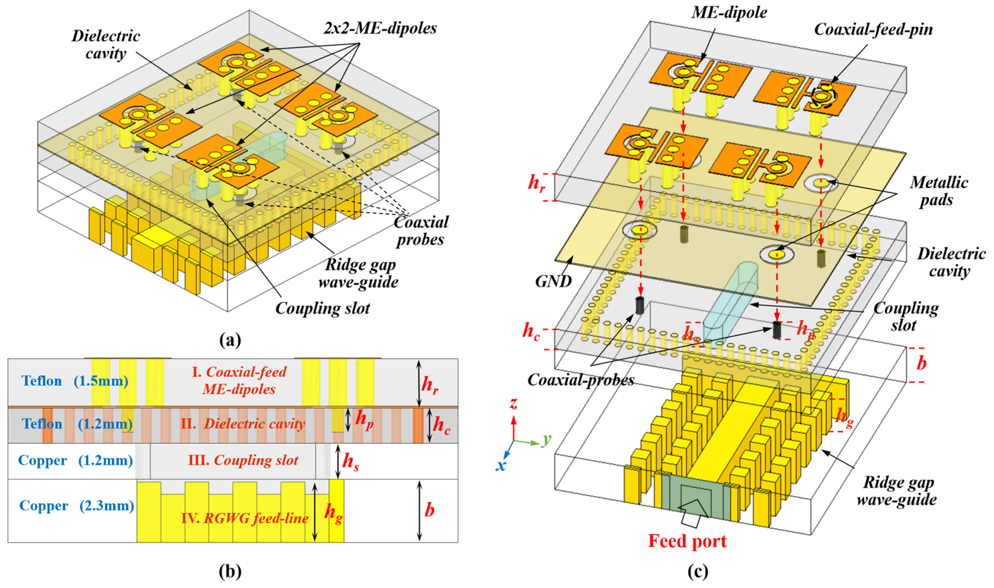
2. The Hybrid-Feed 2 × 2 ME-Dipole Sub-Array

2.1. Configuration

Figure 1 shows the geometry of the proposed 2 × 2 ME-dipole sub-array with a hybrid feed. Figure 2 gives the details of the proposed 2 × 2 ME-dipole sub-array by dividing it into a radiation part and feeding part. The radiation part consists of two Teflon layers with a dielectric constant of 2.1 and tangent loss of 0.001. The two layers have different thicknesses. The four coaxial-feed ME-dipoles on the top layer are modified from the units in the article [13]; a pair of short-end patches and the three pairs of metallics, plated via holes, forms the ME-dipole, and the coaxial-feed T-probe and the gaps between two patches forms a GSG transmission structure, which can excite the ME-dipole. The coaxial-feed line on the top layer is connected with the second layer through a metallic pad. A ring pad is added in the feeding point of the T-probe to realize wide-band impedance matching of the ME-dipole. The second layer is the dielectric cavity with four metallic probes. The four pins with depth of hp are concentric with the feed-pin on the top layer; the metallic pads between the feed-pins and coaxial probes act as the impedance-matching section. The feeding part is on the lower two layers; the third layer and forth layer is the air-filled coupling slot and the short-end RGWG section, which are both made of copper.

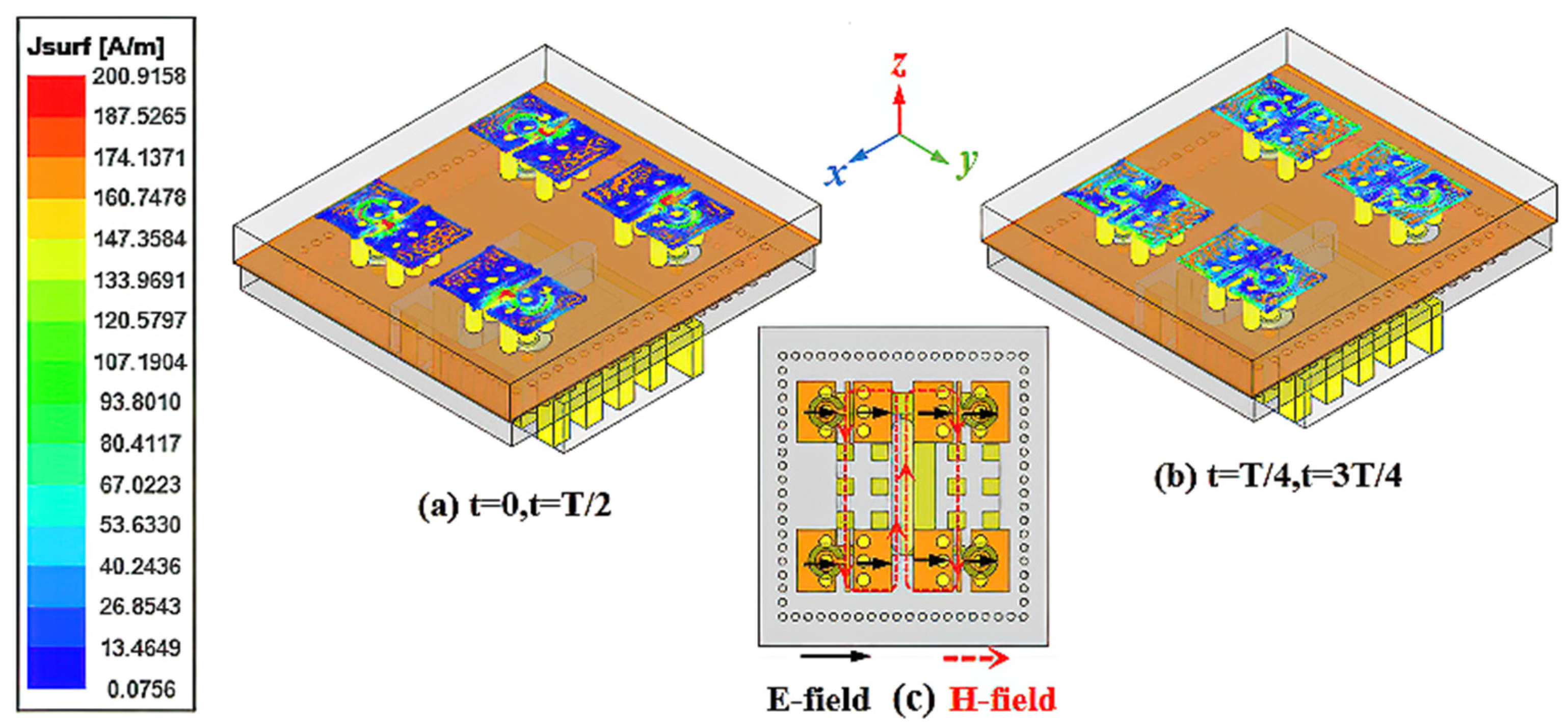
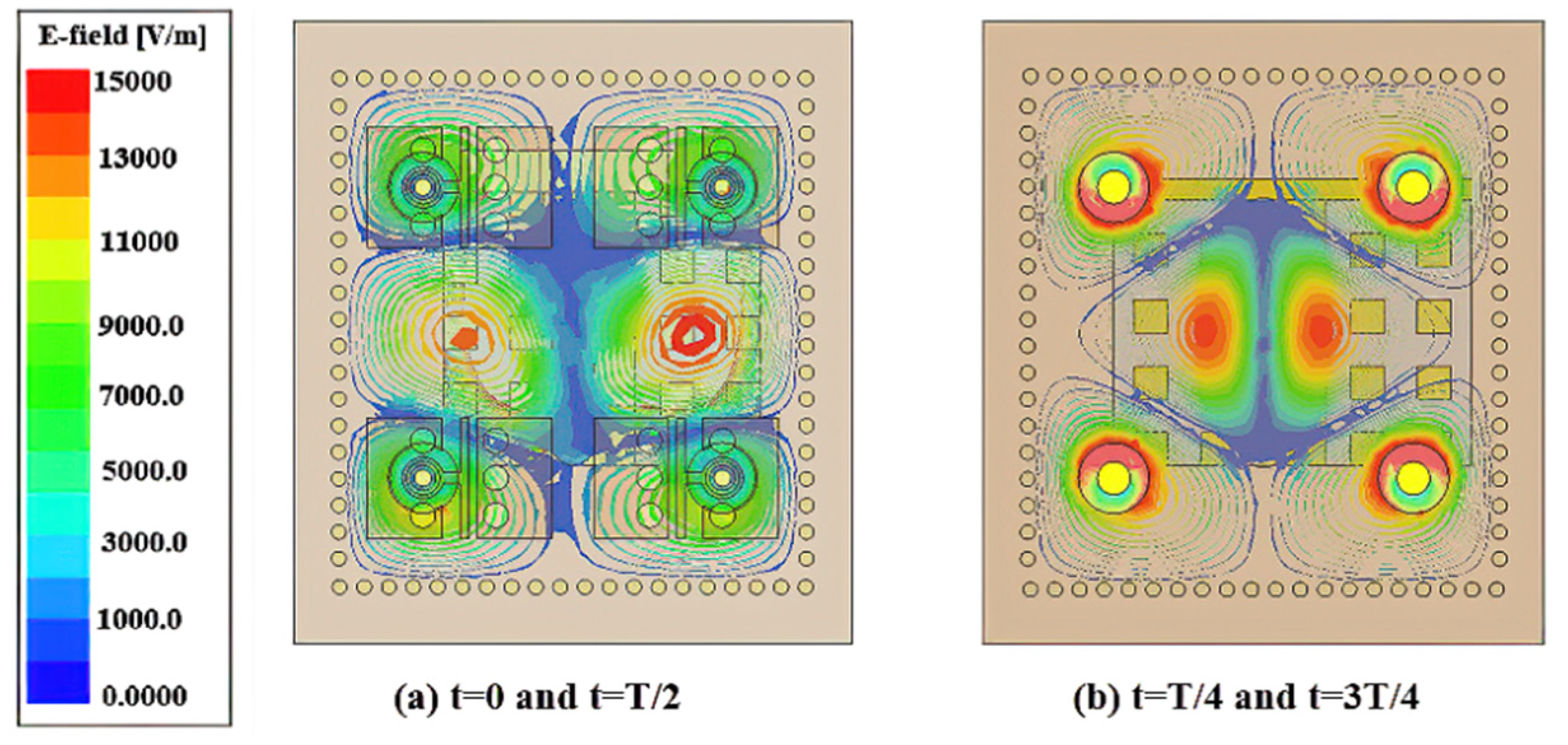
2.2. Operation Mechanism

In order to analyze the working principle of the coaxial-feed ME-dipole, the full-wave simulation software ANSYS Electronics Desktop was used. The simulated surface current distributions on the 2 × 2-ME-dipole sub-array are shown in Figure 3. T represents a period of time; it can be seen that at t = 0 and t = T/2, the current on the inner GSG feed (T-shape probe and the gaps between two patches) are dominant, which indicates that the quarter-wavelength apertures are excited, equivalent to x-direction magnetic-dipoles. On the other hand, when t = T/4 and t = 3T/4, the currents are mainly concentrated on both sides of the quarter-wavelength short-end patches along the y-direction, which indicates that the x-direction electric dipoles are excited. The electric dipoles and the magnetic dipoles are excited alternatively, which forms the ME-dipole sub-array.
The main function of the feeding part is to excite the 2 × 2-unit ME-dipole through the 1-to-4 power divider, which is composed of the dielectric cavity and coaxial probes. Figure 4 exhibits the simulated electric-field distributions in the dielectric cavity. The cavity is excited by the offset slot etched on the top of the short-end RGWG. The coupling slot is on the central part of the cavity and the TE230 mode is excited in the dielectric cavity. The EM-wave feed from the RGWG is evenly intercepted by the coaxial probe through the TE230 mode, and then fed into the ME-dipole sub-array. At each quarter in the period, the electric-field amplitude around the four coaxial probes are nearly equal; the phase is opposite to the y-axis. Therefore, by placing the radiation units on both sides of the y-axis symmetrically, the equal amplitude in-phase radiation of the elements in the sub-array can be realized.

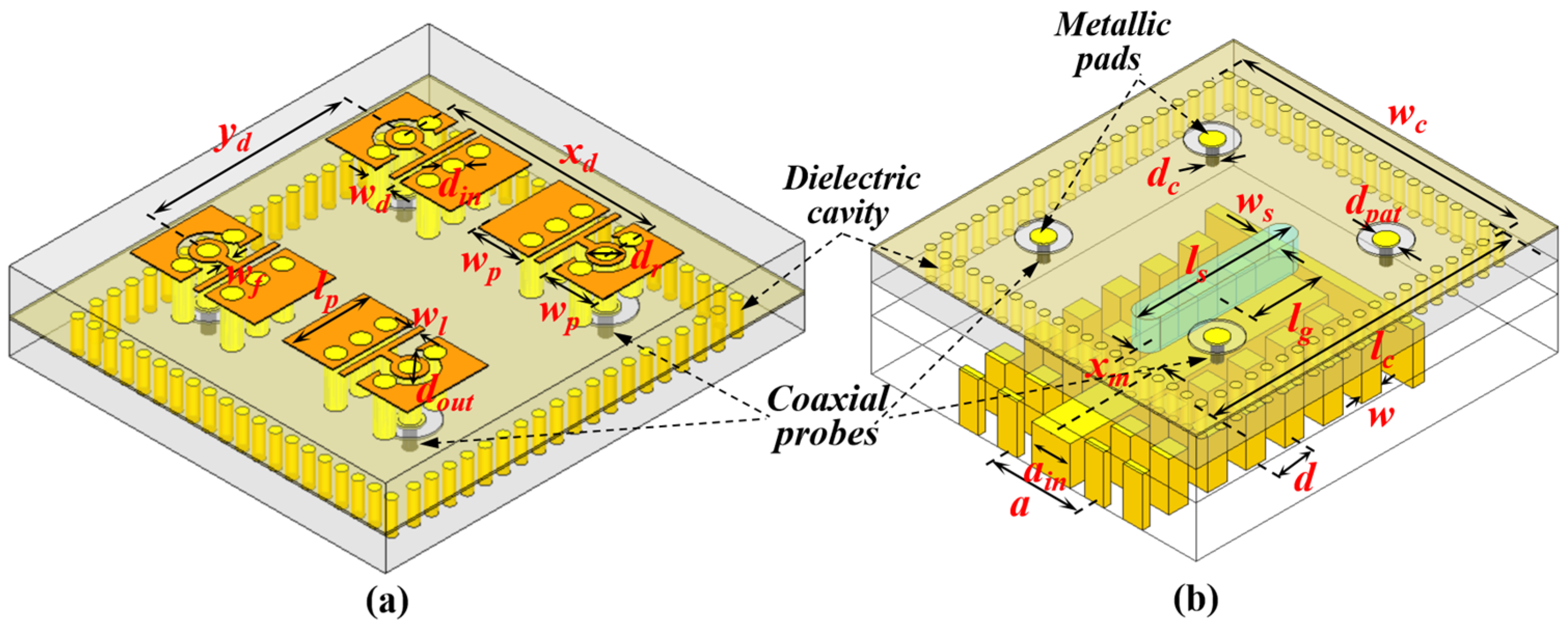
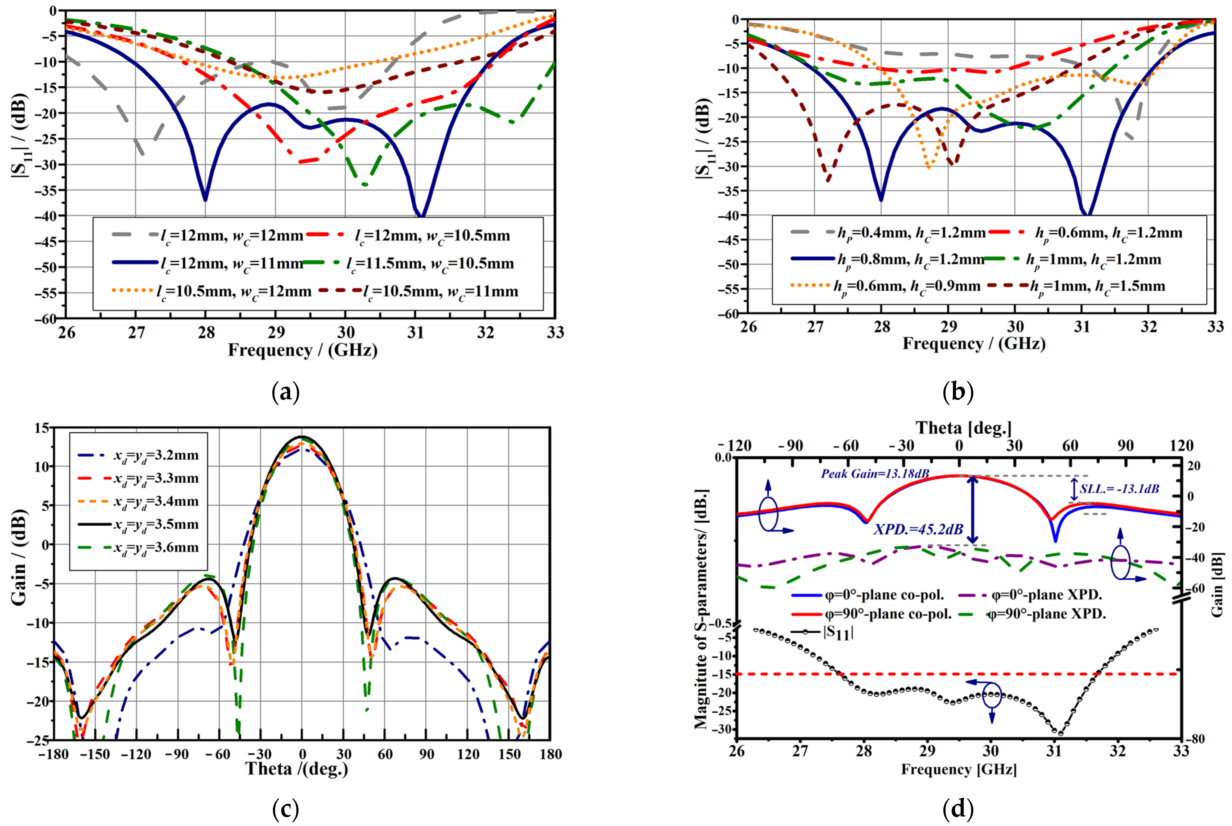
2.3. Performance and Parametric Analysis

The operation mechanism of the proposed 2 × 2-unit ME-dipole sub-array has been studied in the previous section. Performance of the radiation part and the feeding part of the ME-dipole sub-array are discussed, respectively, in this section. In addition, several key parameters of the ME-dipole sub-array will be analyzed to give the design guidelines of the antenna. The original dimensions of the single ME-dipole are as follows: the height of the substrate is nearly λg/4, where the λg is the guide wavelength of the substrate. The length of the single ME-dipole (lp) is set to 0.5 λg, the width of each short-end patch (wp) is set to 0.2 λg and the gap (wd) between the two patches is set to 0.1 λg, which forms an electric dipole. The diameter of the metallic vi as was set to 0.6 mm; accordingly, the diameter of the hole on the ground plane was set to 5.6 mm, forming a 50-ohm coaxial feed line. A pad structure is introduced into the transition between the T-shape MS-line probe and the coaxial-line to replace the direct MS-line transition. The widths of the MS-line T-shape probes are set to 0.28 mm and 0.2 mm.
As illustrated in Figure 5a–c, the resonant frequencies are mainly controlled by the dimension of the short-end patches (lp, wp, wd). Besides, the diameter of the pads also affects the impedance matching bandwidth, which is shown in Figure 5d. By tuning these key parameters, good performance can be achieved for the ME-dipole. Figure 6 gives the radiation patterns and |S11| curves of the optimized ME-dipole, in this paper and [13]; it can be seen that the modified ME-dipole in this paper has a better impedance matching bandwidth, which is beneficial for a sub-array design.
The main function of the hybrid-feed structure is to divide the EM-wave that couples from the offset slot to the coaxial probes through the resonant mode in the dielectric cavity. The first step is to choose the appropriate resonant mode. When the coupling slot is in the center of the cavity, the TE230 mode is the lowest resonant mode that can realize the uniform excitation of the four coaxial probes. The relationship between the dimension of the cavity and the resonant mode can be summarized as follow:
f m n p = 1 2 μ ε m w c 2 + n l c 2 + p h c 2
where wc, lc and hc is the width, length, and height of the cavity; the original value of the three parameters are set to 12 mm, 11.3 mm, and 1.2 mm. According to (1), choosing the dielectric cavity instead of the air-filled cavity can reduce the size of the cavity, which is helpful to reduce the spacing between the adjacent sub-arrays in a large-scale array design. Considering the influence of the metallic vi as, the length and width of the dielectric cavity were analyzed. The results are shown in Figure 7a. The parameter analysis of the height of the dielectric cavity (hc) and the depth of the coaxial-probe (hp) are depicted in Figure 7b. Results show that the value of hc determines the resonant frequency. In addition, the bandwidth is the widest when the ratio of hp to hc is 2/3 and hc is 1.2 mm.
The second step is to set the spacing between the adjacent ME-dipoles in the x- and y-direction. Figure 7c shows the simulated radiation patterns of the sub-array under different xd and yd values. With the increase in the spacing, the gain of the sub-array gradually increases, and the side-lobe level also rises. When xd = yd = 3.5 mm, the peak gain is achieved. The last step is to choose the dimension of the coupling slot; the slot length (ls), width (ws), height (hs), and offset (xm) values affect the impedance matching bandwidth. The parameter adjustment process is similar to that in [15,21]. Following the above design guidelines, a good impedance matching bandwidth of the sub-array can be achieved.
The optimized details of the sub-array are listed in Table 1. The simulated feeding and radiation performance of the optimized sub-array are depicted in Figure 7d. Results show that the |S11|< −10 dB bandwidth is from 26.9 GHz to 32.1 GHz, with a relative bandwidth of 17.9%. The realized gain of the sub-array at 29 GHz is 13.58 dBi, with a radiation efficiency of 90%. The side-lobe level is −13.2 dB and the cross-polarization discrimination (XPD) is 45.4 dB. The simulation results indicate that the proposed hybrid-feed ME-dipole sub-array has a wide impedance-matching bandwidth with good radiation performance. In addition, the hybrid-fed sub-array is the key part to combine the wide-band coaxial-feed ME-dipoles with the low-loss and low-cost gap waveguide feed-network, which is suitable for a large-scale mm-wave antenna array design.

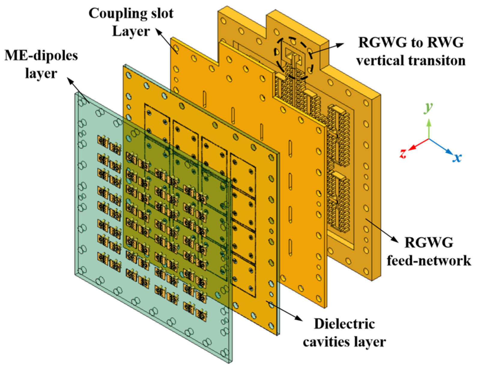
3. Design and Measurement of the 8 × 8-Unit ME-Dipole Antenna Array

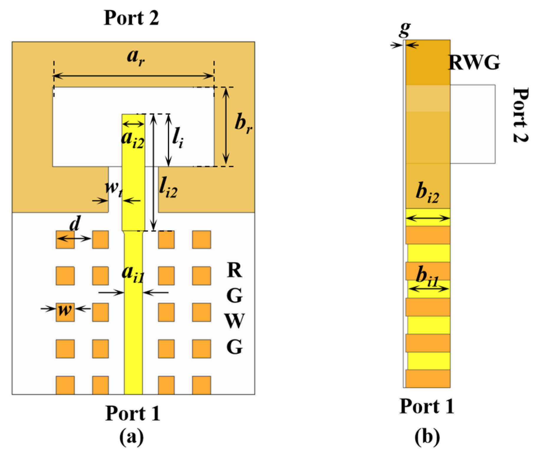
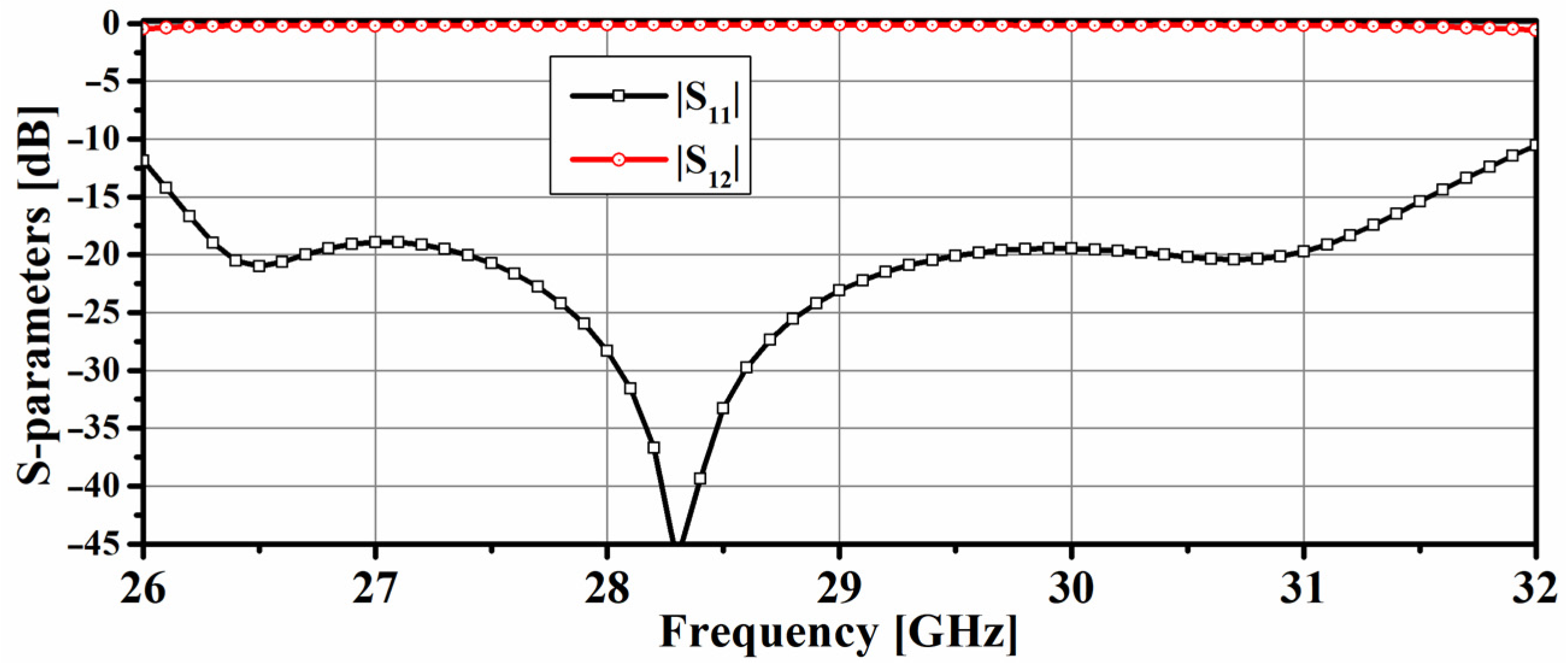
3.1. RGWG Feed Network Design and Array Configuration

Based on the proposed 2 × 2-ME-dipole sub-array, an 8 × 8-unit ME-dipole antenna array was designed and fabricated. The proposed 8 × 8 ME-dipole array is fed by a 1-to-16 RGWG corporate-feed network. The distance between the neighboring sub-arrays are 12.8 mm (1.28 λ0) in both the x-direction and y-direction. The basic unit of the feed network is an equal power RGWG H-plane T-junction, as shown in Figure 8a. Three RGWG sections are introduced into the RGWG H-T as the impedance transformers. The power splitting ratio of the output ports and the impedance matching bandwidth of the input port can be tuned by adjusting the ridge height and length of the three RGWG sections. It is worth mentioning that by adjusting the power splitting ration based on this method, the phase difference between the output ports can be controlled within a small range. Figure 8b exhibits the simulated S-parameters of the equal power RGWG H-T and unequal power RGWG H-T-junction (power-splitting ration = 3.5 dB). Results show that the phase difference between the output ports is within ±5° and the |S11| is less than −15 dB over the frequency band from 26 GHz to 36 GHz for the two RGWG H-T-junctions.
The total 1-to-16 feed-network is shown in Figure 9a, and the simulated performance of the feed-network is shown in Figure 9b; the phase and amplitude differences among all the output ports are within ±5° and ±0.2 dB; and the |S11| of the input port is less than −17.5 dB, covering the bandwidth of 26 GHz~32 GHz. Tolerance of the gap height is also simulated and verified, and the results are depicted in Figure 6. Results shows that the designed feed network still works normally within the gap height error range of ±0.04 mm.

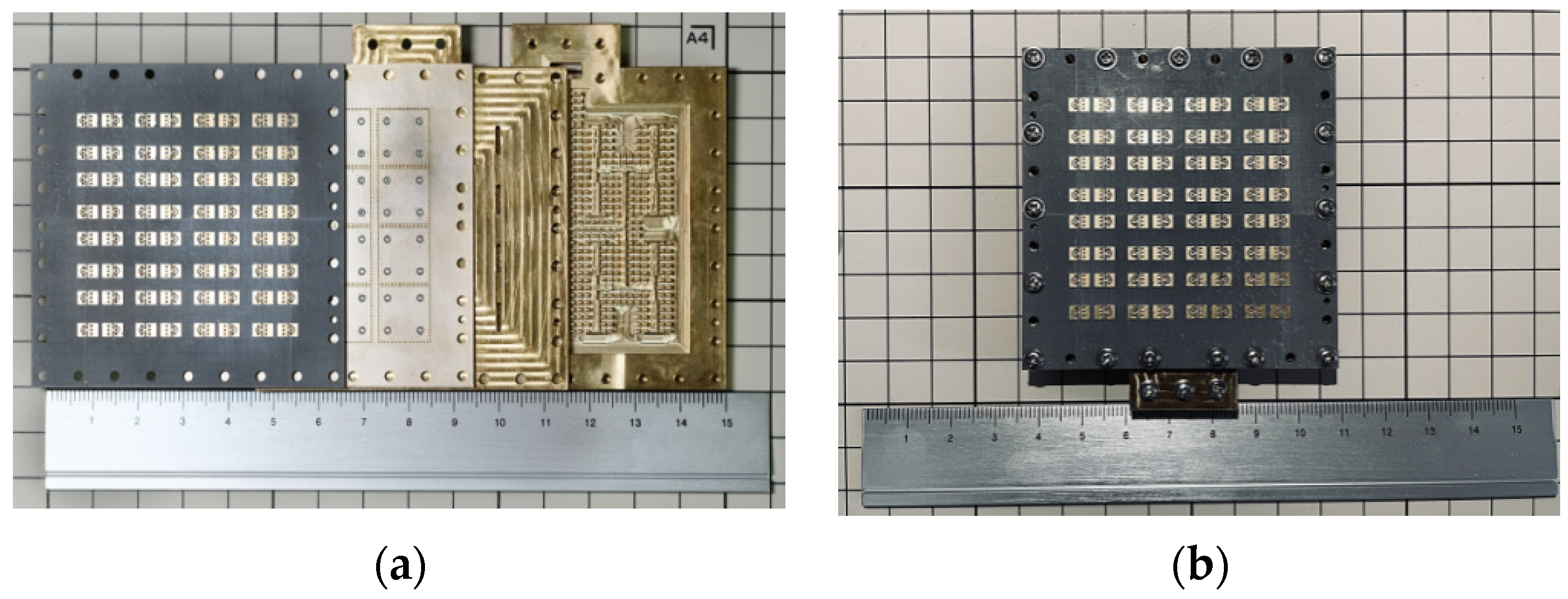
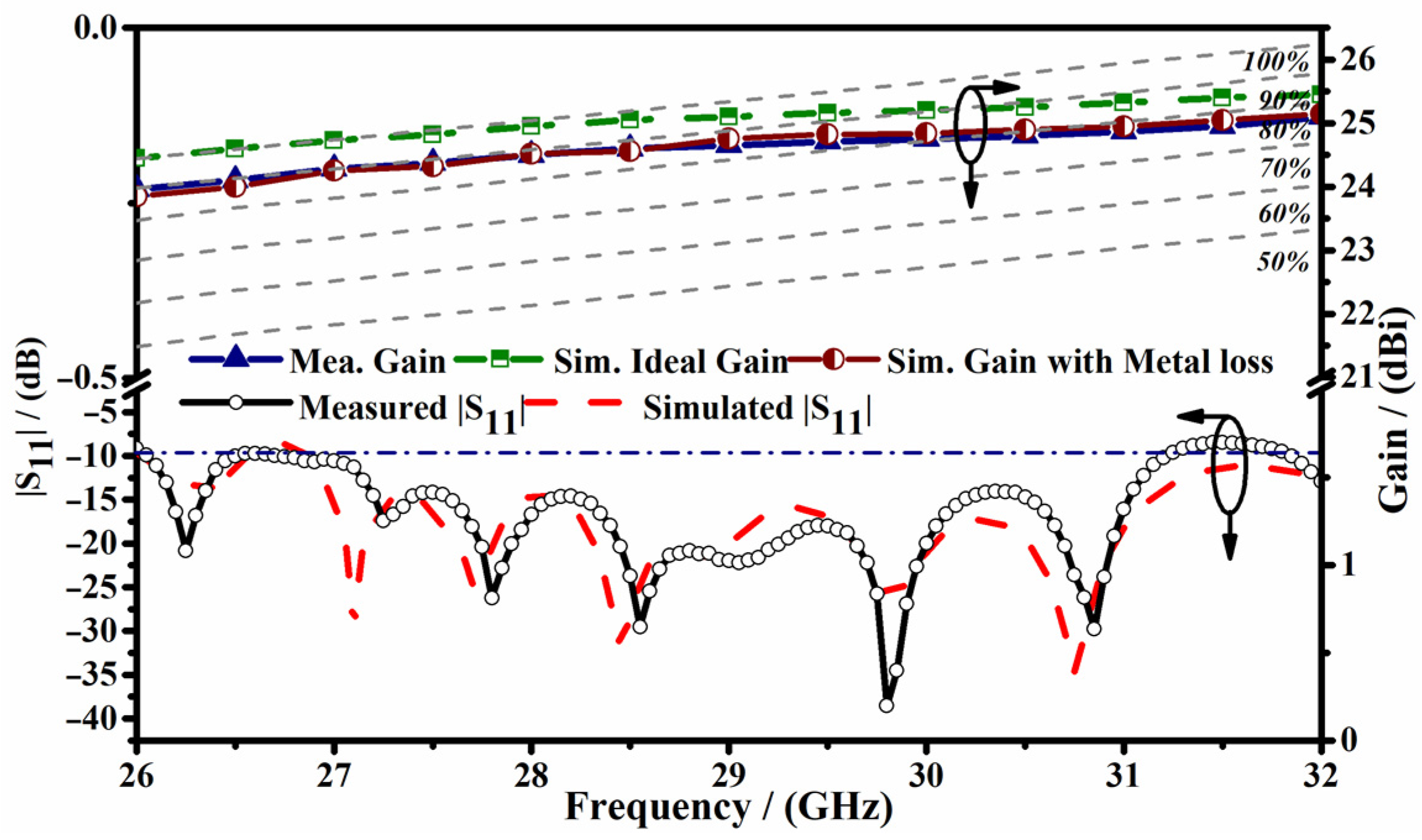
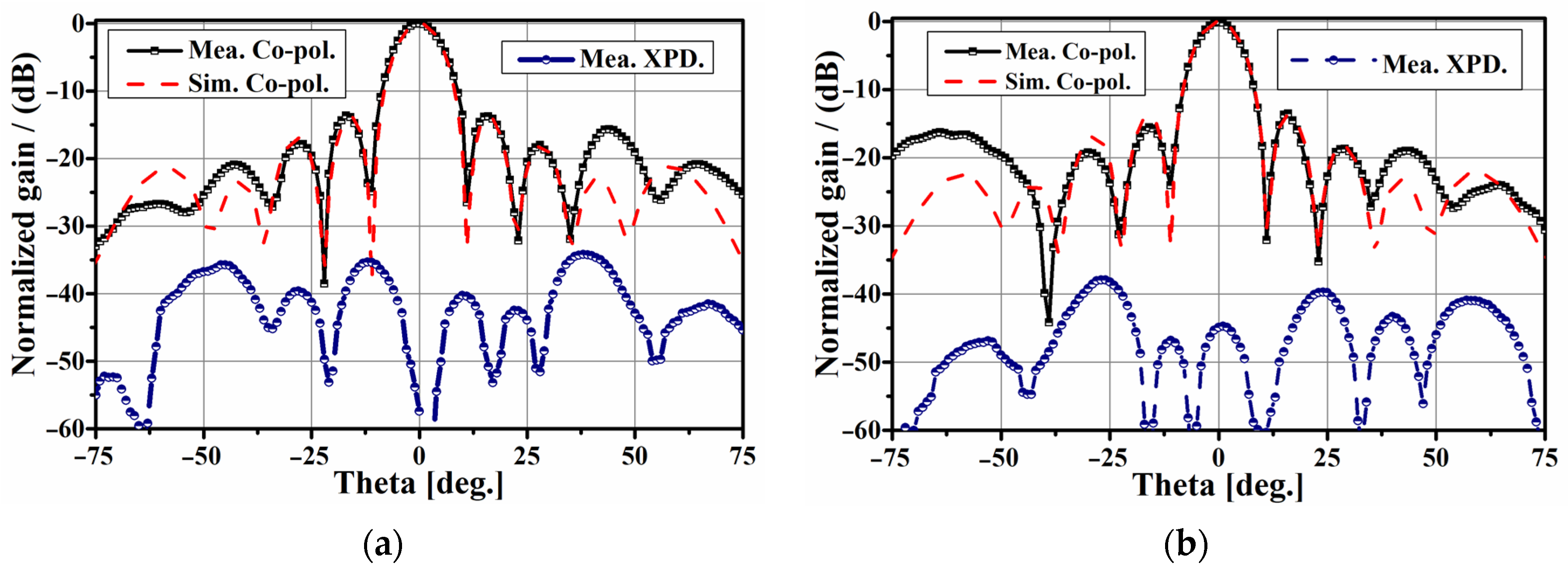
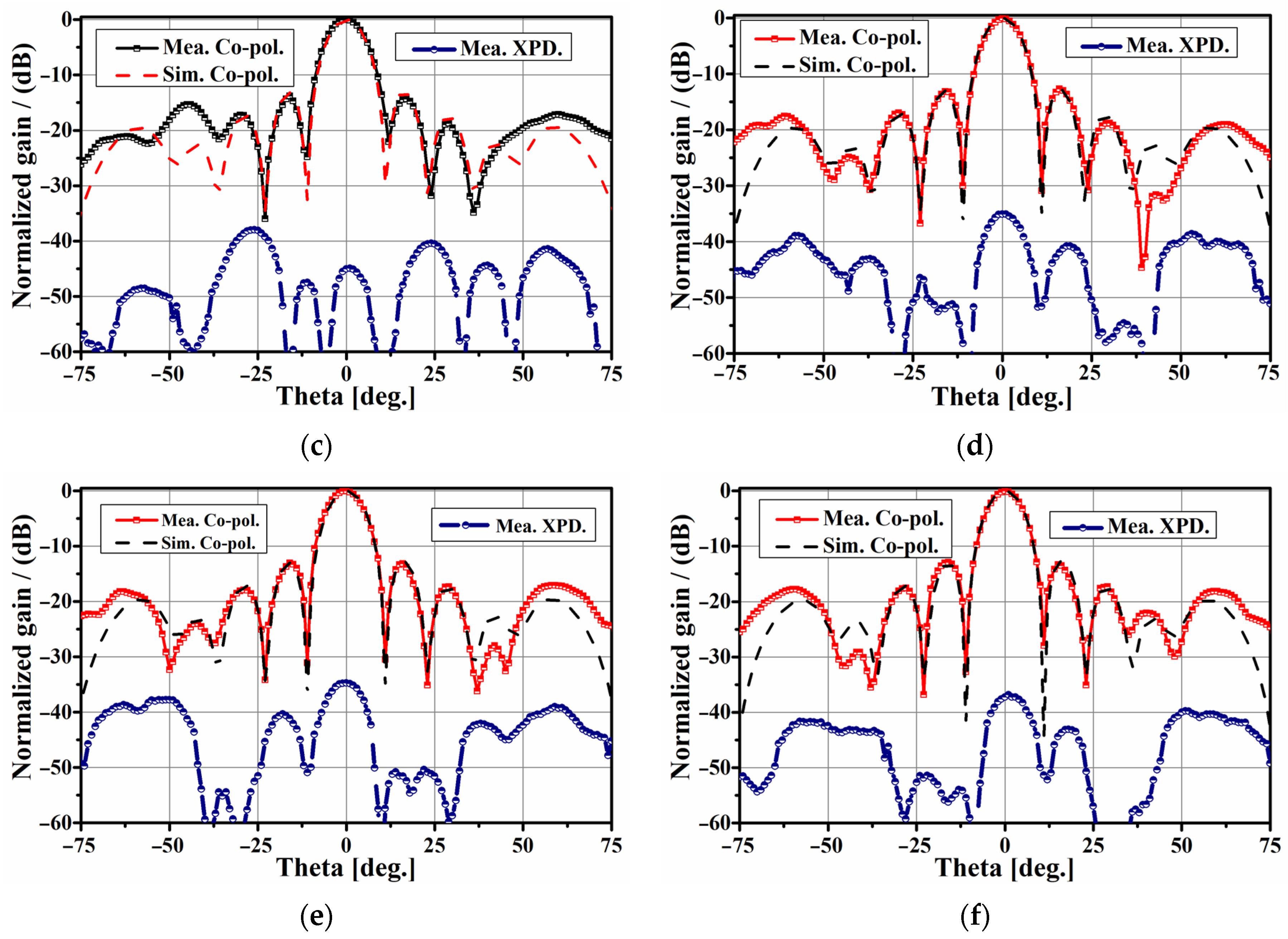
3.2. Measurement of the 8 × 8-Unit ME-Dipole Antenna Array

In order to verify the validity of the proposed antenna array, a prototype of the 8 × 8-unit hybrid-feed ME-dipole antenna array prototype was fabricated and tested. The configuration and photograph of the 8 × 8-unit hybrid-feed ME-dipole antenna array is shown in Figure 10. The radiation part is made of two Teflon layers with a thickness of 1.6 mm and 1.2 mm. The feeding part is located in lower two layers, which are made of copper with a thickness of 1.2 mm and 2.1 mm. A ridged gap waveguide to WR-30 rectangular waveguide vertical transition was invented as the feed port, which is shown in Figure 11. The optimized structure dimensions are shown in Table 2. The S-parameters of the vertical transition is shown in Figure 12. Results indicate that the transition structure has a reflection coefficient of less than −15 dB in the frequency range of 26.2 to 31.4 GHz, and the insertion loss of the transition is less than 0.05 dB in the same frequency range. The total size of the array is 67.5 mm × 67.5 mm × 6.25 mm, and the effective radiation size is 56 mm × 56 mm.
The fabricated prototype of the 8 × 8-unit hybrid-feed ME-dipole array is shown in Figure 13. The radiation part is made up of low-cost PCB technique and the two layers are bonded by conductive adhesive process. Metallic air-filled holes are used to replace the metallic pins in the array. The feed network of the array was made up of copper and machined by CNC milling; the smallest size was 0.5 mm. The radiation part and the feeding part was assembled by eight M2 screws. Two 1.6 mm in diameter locating pins were used to align the four layers, so as to ensure the alignment error can be controlled within ±0.02 mm. Tolerance of the array was analyzed by the full-wave simulation software HFSS, to ensure a better performance of the array.
The reflection coefficient of the fabricated array was measured by a Keysight E8361A VNA and the radiation performance was measured by a mm-wave far-field antenna measurement system, which is shown in Figure 14. The measured and simulated reflection coefficient are plotted in Figure 15. The measured bandwidth with |S11| < −10 dB is from 26.05 GHz to 31.15 GHz. The trend of the measured curve is in good agreement with the simulated results. The measured and simulated gain vs. frequency curves are also given in Figure 15. The measured maximum gain is 25.15 dBi and the maximum radiation efficiency is 89% over the operation bandwidth. A 0.4 dB gain difference can be observed between the measured and simulated ideal gain, which may mainly be caused by the surface roughness of the feed network and the fabrication error. In order to verify the gain difference, the metal surface roughness and fabrication error are all calculated into the electric conductivity of the copper that is used in feed network; the value is 4.2 × 10⁷ S/m. The simulated gain vs. frequency curve under this situation is also given in Figure 15. It has good consistency with the measured curve, which indicates that the estimation result can be used in a large-scale array design.
The measured radiation patterns in the E-plane and H-plane are shown in Figure 16. The stable radiation patterns can be observed over the operation band from 27 GHz to 31 GHz. The measured first side-lobe levels are less than −12.5 dB in both the E-plane and H-plane, respectively, with the cross-polarization level better than 35 dB in both planes.

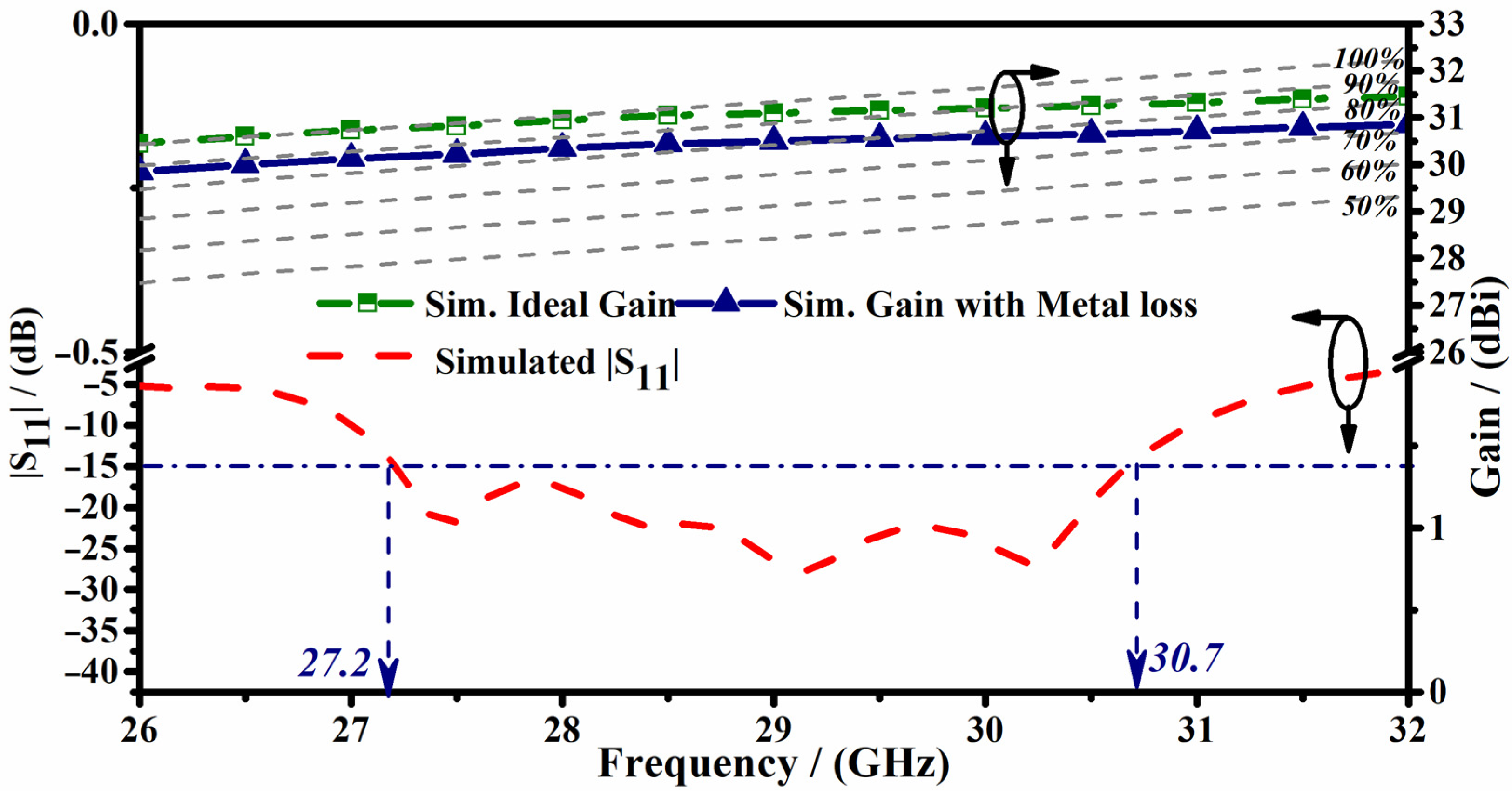
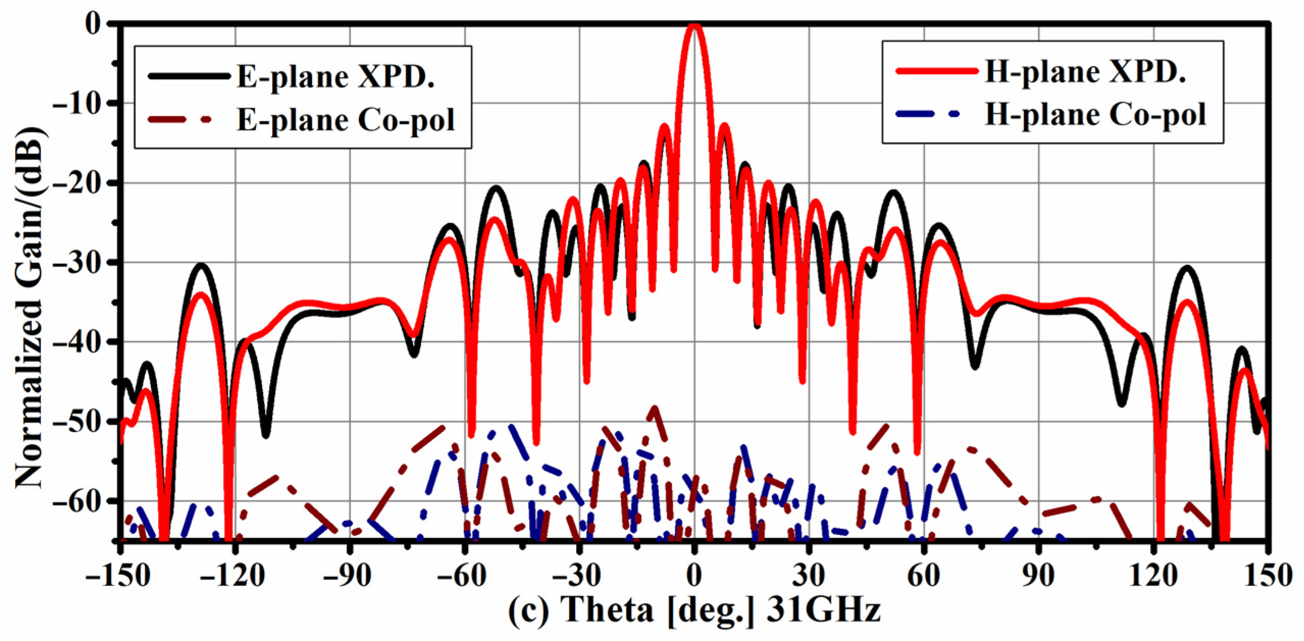
4. Analysis and Comparison of the Hybrid-Feed ME-Dipole Antenna Array

Based on the measurement results of the 8 × 8-unit hybrid-feed ME-dipole array, a 16 × 16-unit hybrid-feed ME-dipole array was further designed and simulated. The configuration of the 16 × 16-unit ME-dipole antenna array is shown in Figure 17.
The simulated feeding and radiation performance of the 16 × 16-unit ME-dipole antenna array are shown in Figure 18. The influence of machining error and metal surface roughness on array performance can be summarized as the decrease in metal conductivity used in feed-network. The conductivity of the copper used in feed-network is set to 4.2 × 10⁷ S/m, which is equal to the value derived from the measured results of the 8 × 8-unit hybrid-feed ME-dipole array. Simulated results shows that the relative bandwidth with |S11| < −15 dB is 12%. The simulated gain of the 16 × 16 array is higher than 30.13 dBi over the band of 27 GHz to 31 GHz, with the radiation efficiency better than 76%. The simulated E-plane and H-plane radiation patterns are given in Figure 19a–c. The first side-lobe level of both planes at 27 GHz, 29 GHz, and 31 GHz are lower than −13 dB and the XPD are all better than 35 dB. The simulated results indicate that the proposed planar array has wide-band and high-efficiency features.
Table 3 lists the performance comparison of the planar mm-wave antenna arrays, including the fabrication technology, impedance matching bandwidth, maximum gain, radiation efficiency, XPD, array dimensions, and fabrication cost. By comparison with the substrate-integrated coaxial line slot array in [7] and printed GWG feed slot array in [6], the proposed antenna array in this work has a wider bandwidth and higher radiation efficiency. The ME-dipole array fed by gap waveguide or SIW are fabricated by PCB technology in [10,11,19]; the three antennas have a good impedance-matching bandwidth with a low fabrication cost. However, the insertion loss caused by the substrate-based feed network increases with the expansion of the array scale, which reduces the radiation efficiency of the large-scale array antennas. Furthermore, the LTCC process used in [10] also has a high fabrication cost. The full corporate-feed slot array in [15] has a better radiation efficiency with a wide-band feature but the diffusion bonding process costs high. The pure GWG slot antenna array in [18] has a high radiation efficiency with reduced fabrication cost, but the bandwidth is narrow. In addition, the antenna array in [21] combine the ME-dipole with the GWG feed network, but the aperture efficiency is limited since the feed network occupies much of the radiation aperture. By comparison with the aforementioned antenna arrays, the proposed hybrid-feed ME-dipoles antenna array in this paper gives an approach for a wide-band, high-efficiency, large-scale antenna array with moderate fabrication cost.

5. Conclusions

A low fabrication cost hybrid-feed ME-dipole antenna array with wide-band high-efficiency features for a mm-wave large-scale array design is presented in this paper. A novel hybrid-feed 2 × 2-unit ME-dipole sub-array combine the coaxial-feed ME-dipoles with an aperture-coupled dielectric cavity is proposed as the basic unit of the array. A 16 × 16-unit and an 8 × 8-unit antenna array were designed, and the latter array was fabricated. The corporate-feed network built by the new RGWG H-T-junction was adopted to feed the arrays. The total array can be fabricated by low-cost PCB technology, CNC milling, and assembled without any expensive bonding process. The measured results show that the proposed array can achieve a relative bandwidth of 18% with |S11| < −10 dB and a maximum radiation efficiency of 80%. The proposed hybrid-feed ME-dipole antenna array has potential in mm-wave wireless system applications that require large-scale arrays.

Author Contributions

Conceptualization, W.T. and H.L.; methodology, H.L. and Y.X.; software, W.T., C.L. and K.Z.; validation, C.L. and W.T.; formal analysis, H.L. and C.L.; investigation, C.L.; resources, W.T.; data curation, W.T., K.Z., and H.L.; writing—original draft preparation, W.T.; writing—review and editing, H.L. and Y.X.; visualization, W.T. and H.L.; supervision, H.S.; project administration, H.L.; funding acquisition, H.L. and Y.X. All authors have read and agreed to the published version of the manuscript.

Funding

This research was funded by the Natural Science Foundation of China under Grant (62001522), supported by the Beijing Key Laboratory of Millimeter Wave and Terahertz Techniques (Corresponding author: Hao Luo).

Conflicts of Interest

The authors declare no conflict of interest.

References

  1. Hong, W.; Jiang, Z.H.; Yu, C.; Zhou, J.; Chen, P.; Yu, Z.; Zhang, H.; Yang, B.; Pang, X.; Jiang, M.; et al. Multibeam antenna technologies for 5G wireless communications. IEEE Trans. Antennas Propag. 2017, 65, 6231–6249. [Google Scholar] [CrossRef]
  2. Hasch, J.; Topak, E.; Schnabel, R.; Zwick, T.; Weigel, R.; Waldschmidt, C. Millimeter-Wave Technology for Automotive Radar Sensors in the 77 GHz Frequency Band. IEEE Trans. Microw. Theory Tech. 2012, 60, 845–860. [Google Scholar] [CrossRef]
  3. Zankl, D.; Schuster, S.; Feger, R.; Stelzer, A.; Scheiblhofer, S.; Schmid, C.M.; Ossberger, G.; Stegfellner, L.; Lengauer, G.; Feilmayr, C.; et al. BLASTDAR—A Large Radar Sensor Array System for Blast Furnace Burden Surface Imaging. IEEE Sens. J. 2015, 15, 5893–5909. [Google Scholar] [CrossRef]
  4. Sohrabi, F.; Yu, W. Hybrid Analog and Digital Beamforming for mmWave OFDM Large-Scale Antenna Arrays. IEEE J. Sel. Areas Commun. 2017, 35, 1432–1443. [Google Scholar] [CrossRef] [Green Version]
  5. Wu, Y.W.; Hao, Z.C.; Miao, Z.W. A Planar W-Band Large-Scale High-Gain Substrate-Integrated Waveguide Slot Array. IEEE Trans. Antennas Propag. 2020, 68, 6429–6434. [Google Scholar] [CrossRef]
  6. Jiang, X.; Jia, F.; Cao, Y.; Huang, P.; Yu, J.; Wang, X.; Shi, Y. Ka-Band 8 × 8 Low-Sidelobe Slot Antenna Array Using a 1-to-64 High-Efficiency Network Designed by New Printed RGW Technology. IEEE Antennas Wirel. Propag. Lett. 2019, 18, 1248–1252. [Google Scholar] [CrossRef]
  7. Qi, Z.; Li, X.; Xiao, J.; Zhu, H. Low-Cost Empty Substrate Integrated Waveguide Slot Arrays for Millimeter-Wave Applications. IEEE Antennas Wirel. Propag. Lett. 2019, 18, 1021–1025. [Google Scholar] [CrossRef]
  8. Liu, B.; Zhao, R.; Ma, Y.; Guo, Z.; Wei, X.; Xing, W.; Wang, Y. A 45° Linearly Polarized Slot Array Antenna With Substrate Integrated Coaxial Line Technique. IEEE Antennas Wirel. Propag. Lett. 2018, 17, 339–342. [Google Scholar] [CrossRef]
  9. Luk, K.M.; Hang, W. A new wideband unidirectional antenna element. Int. J. Microw. Opt. Technol. 2006, 1, 35–44. [Google Scholar]
  10. Li, Y.; Luk, K.M. A 60-GHz Wideband Circularly Polarized Aperture-Coupled Magneto-Electric Dipole Antenna Array. IEEE Trans. Antennas Propag. 2016, 64, 1325–1333. [Google Scholar] [CrossRef]
  11. Li, Y.; Wang, C.; Guo, Y.X. A Ka-Band Wideband Dual-Polarized Magnetoelectric Dipole Antenna Array on LTCC. IEEE Trans. Antennas Propag. 2020, 68, 4985–4990. [Google Scholar] [CrossRef]
  12. Sun, J.; Li, A.; Luk, K.-M. A High-Gain Millimeter-Wave Magnetoelectric Dipole Array with Packaged Microstrip Line Feed Network. IEEE Antennas Wirel. Propag. Lett. 2020, 19, 1669–1673. [Google Scholar] [CrossRef]
  13. Ng, K.B.; Wong, H.; So, K.K.; Chan, C.H.; Luk, K.M. 60 GHz Plated Through Hole Printed Magneto-Electric Dipole Antenna. IEEE Trans. Antennas Propag. 2012, 60, 3129–3136. [Google Scholar] [CrossRef]
  14. Kim, D.; Zhang, M.; Hirokawa, J.; Ando, M. Design and Fabrication of a Dual-Polarization Waveguide Slot Array Antenna with High Isolation and High Antenna Efficiency for the 60 GHz Band. IEEE Trans. Antennas Propag. 2014, 62, 3019–3027. [Google Scholar] [CrossRef]
  15. Tomura, T.; Hirokawa, J.; Hirano, T.; Ando, M. A 45 degrees Linearly Polarized Hollow-Waveguide16 × 16-Slot Array Antenna Covering 71-86 GHz Band. IEEE Trans. Antennas Propag. 2014, 62, 5061–5067. [Google Scholar] [CrossRef]
  16. Kildal, P.-S.; Alfonso, E.; Valero-Nogueira, A.; Rajo-Iglesias, E. Local Metamaterial-Based Waveguides in Gaps between Parallel Metal Plates. IEEE Antennas Wirel. Propag. Lett. 2008, 8, 84–87. [Google Scholar] [CrossRef]
  17. Ferrando-Rocher, M.; Herranz-Herruzo, J.I.; Valero-Nogueira, A.; Bernardo-Clemente, B.; Herranz, J.I.; Bernardo, B. Full-Metal K-Ka Dual-Band Shared-Aperture Array Antenna Fed by Combined Ridge-Groove Gap Waveguide. IEEE Antennas Wirel. Propag. Lett. 2019, 18, 1463–1467. [Google Scholar] [CrossRef]
  18. Ferrando-Rocher, M.; Herranz-Herruzo, J.I.; Valero-Nogueira, A.; Vila-Jimenez, A. Single-Layer Circularly-Polarized Ka-Band Antenna Using Gap Waveguide Technology. IEEE Trans. Antennas Propag. 2018, 66, 3837–3845. [Google Scholar] [CrossRef]
  19. Sorkherizi, M.S.; Dadgarpour, A.; Kishk, A. Planar High-efficiency Antenna Array Using New Printed Ridge Gap Waveguide Technology. IEEE Trans. Antennas Propag. 2017, 65, 3772–3776. [Google Scholar] [CrossRef]
  20. Cao, B.; Shi, Y.; Feng, W. W-Band LTCC Circularly Polarized Antenna Array With Mixed U-Type Substrate Integrated Waveguide and Ridge Gap Waveguide Feeding Networks. IEEE Antennas Wirel. Propag. Lett. 2019, 18, 2399–2403. [Google Scholar] [CrossRef]
  21. Cao, J.; Wang, H.; Mou, S.; Soothar, P.; Zhou, J. An Air Cavity-Fed Circularly Polarized Magneto-Electric Dipole Antenna Array With Gap Waveguide Technology for mm-Wave Applications. IEEE Trans. Antennas Propag. 2019, 67, 6211–6216. [Google Scholar] [CrossRef]
  22. Li, X.; Xiao, J.; Qi, Z.; Zhu, H. Broadband and High-Gain SIW-Fed Antenna Array for 5G Applications. IEEE Access 2018, 6, 56282–56289. [Google Scholar] [CrossRef]
  23. Ding, Z.-F.; Xiao, S.; Tang, M.-C.; Liu, C.; Shaoqiu, X. A Compact Highly Efficient Hybrid Antenna Array for W-Band Applications. IEEE Antennas Wirel. Propag. Lett. 2018, 17, 1547–1551. [Google Scholar] [CrossRef]
  24. Saeidi-Manesh, H.; Zhang, G. High-Isolation, Low Cross-Polarization, Dual-Polarization, Hybrid Feed Microstrip Patch Array Antenna for MPAR Application. IEEE Trans. Antennas Propag. 2018, 66, 2326–2332. [Google Scholar] [CrossRef]
Figure 1. Geometry of the hybrid-feed 2 × 2-unit ME-dipole sub-array. (a) Perspective view. (b) Side view. (c) Exploded view.
Electronics 10 02383 g001
Figure 2. Details of the hybrid-feed 2 × 2-unit ME-dipole sub-array. (a) Radiation part. (b) Feeding part.
Electronics 10 02383 g002
Figure 3. Simulated surface current distribution of the hybrid-feed 2 × 2-unit ME-dipole sub-array. (a) t = 0, t = T/2. (b) t = T/4, t = 3T/4. (c) Equivalent magnetic currents and electric currents.
Electronics 10 02383 g003
Figure 4. E-field distribution of the feeding part. (a) t = 0 and t = T/2. (b) t = T/4 and t = 3T/4.
Electronics 10 02383 g004
Figure 5. Parameter analysis of the ME-dipole unit. (a) Length of the short-end patches. (b) Width of the short-end patches. (c) Gap width of the short-end patches. (d) Diameter of the pad.
Electronics 10 02383 g005
Figure 6. Performance of the original ME-dipole in [13] and modified ME-dipole in this paper. (a) |S11| curves. (b) Radiation patterns in the E-plane. (c) Radiation patterns in the H-plane.
Electronics 10 02383 g006
Figure 7. Parameter analysis and performance of the sub-array. (a) Length and width of the dielectric cavity. (b) Heights of the dielectric cavity and coaxial probes. (c) Spacing of the ME-dipoles. (d) Optimized performance of the sub-array.
Electronics 10 02383 g007
Figure 8. Geometry of the proposed RGWG H-T divider and simulated performance. (a) The RGWG H-T-junction. (b) Simulated S-parameters of the proposed RGWG H-T-junction.
Electronics 10 02383 g008
Figure 9. Configuration and simulated performance of the 1-to-16 RGWG corporate-feed network. (a) Configuration. (b) Simulated S-parameters.
Electronics 10 02383 g009
Figure 10. Configuration of the 8 × 8 ME-dipole antenna array.
Electronics 10 02383 g010
Figure 11. Vertical transition from RGWG to standard WR-30 RWG. (a) Top view. (b) Side view.
Electronics 10 02383 g011
Figure 12. Simulated S-parameters of the vertical transition.
Electronics 10 02383 g012
Figure 13. Photograph of the fabricated 8 × 8-unit ME-dipole antenna array. (a) Diffusion layers. (b) Assembled prototype.
Electronics 10 02383 g013
Figure 14. Measurement setup. (a) Block diagram of measurement setup. (b) Photograph of the measurement setup.
Electronics 10 02383 g014
Figure 15. Measured and simulated reflection coefficient and gain of the 8 × 8-unit hybrid-feed ME-dipoles antenna array.
Electronics 10 02383 g015
Figure 16. Measured and simulated radiation patterns of the 8 × 8-unit hybrid-feed ME-dipoles antenna array. (a) 27 GHz E-plane. (b) 27 GHz H-plane. (c) 29 GHz E-plane. (d) 29 GHz H-plane. (e) 31 GHz E-plane. (f) 31 GHz H-plane.
Electronics 10 02383 g016aElectronics 10 02383 g016b
Figure 17. Configuration of the 16 × 16-unit hybrid-feed ME-dipole antenna array.
Electronics 10 02383 g017
Figure 18. Simulated performance of the 16 × 16-unit hybrid-feed ME-dipole antenna array.
Electronics 10 02383 g018
Figure 19. Simulated radiation patterns of the 16 × 16-unit hybrid-feed ME-dipole antenna array. (a) 27 GHz. (b) 29 GHz. (c) 31 GHz.
Electronics 10 02383 g019aElectronics 10 02383 g019b
Table 1. Details of the proposed hybrid-feed 2 × 2-unit ME-dipole sub-array (unit: mm).
ParameterValueParameterValue
wd0.85 (0.12 λg)dc0.4 (0.06 λg)
hr1.6 (0.22 λg)hc1.2 (0.17 λg)
din0.6 (0.08 λg)dpat1.7 (0.24 λg)
dout1.6 (0.22 λg)hp0.8 (0.11 λg)
wp1.8 (0.25 λg)wl0.2 (0.03 λg)
lp2.9 (0.4 λg)wf0.28 (0.04 λg)
ws1xd3.6 (0.5 λg)
ls6.5yd3.6 (0.5 λg)
wc11 (1.54 λg)a3.6
lc12 (1.7 λg)b2.1
hs1.2ain1.6
hg2xm0.7
lg5w0.8
d1.6dr1
Table 2. Details of the vertical transition from RGWG to standard WR-30 RWG (unit: mm).
ParameterValueParameterValue
ar7.112br3.556
ai21bi22
ai10.8li25.1
bi11.9G0.1
d1.6W0.8
wt0.6li2.3
Table 3. Performance comparison of the presented mm-wave planar antenna arrays (unit: mm).
Ref.Bandwidth
(|S11| < −10 dB)
Num. of UnitArray Size
0)
Fabrication ProcessMax.
Gain
Max. Rad.
Efficiency
Aperture
Efficiency *
XPD.
(dB)
Cost
[6]16%
34–40.1 GHz
8 × 86.4 × 6.4 × 0.17PCB24 dBi41.7%48.8%30Low
[8]2.6%
33.95–34.86 GHz
5 × 65.07 × 3.82 × 0.1PCB17.09 dBi22%21.02%26.8Low
[10]18%
55.4–66.5 GHz
8 × 86.12 × 6.8 × 0.5Multi-layer PCB26.1 dBi70%95.8%20Med.
[11]45%
25.5–40.2 GHz
4 × 42 × 2 × 0.12LTCC16.1 dBi83%81%15High
[15]20%
71–86 GHz
16 × 1615.7 × 16 × 0.8Diffusion bonding32.9 dBi86.6%61.7%30High
[18]3.6%
29.6–30.7 GHz
4 × 45.3 × 5.3 × 1.1Machining22.4 dBi99%49.2%13Med.
[19]16.5%
28.8–34 GHz
4 × 43.5 × 3.4 × 0.3PCB21.2 dBi70%88%35Low
[21]16.4%
86.7–102.2 GHz
4 × 811.8 × 11.4 × 2.2PCB + machining23 dBiN.A.11.8%15Med.
This work16.4%
26.05–31.15 GHz
8 × 85.4 × 5.4 × 0.6PCB + machining25 dBi85%86.2%34Med.
This work13.8% **
27.1–31.1 GHz
16 × 1610.8 × 10.8 × 0.6PCB + machining31 dBi **83.2% **85.8% **37Med.
* The aperture efficiency can be calculated as η = G λ 0 / ( 4 π A e ) , where G is the gain, λ0 is the wavelength at the central frequency, and Ae is the physical aperture area of the array [7]. ** Simulated results.
Publisher’s Note: MDPI stays neutral with regard to jurisdictional claims in published maps and institutional affiliations.

