Abstract
In photovoltaic (PV) systems, maximum power point (MPP) is tracked by matching the load impedance to the internal impedance of the PV array by adjusting the duty cycle of the associated DC-DC converter. Scientists are trying to improve the efficiency of these converters by improving the performance of the power stage, while limited attention is given to finding alternative methods. This article describes a novel supercapacitor (SC) assisted technique to enhance the efficiency of a PV system without modifying the power stage of the charge controller. The proposed system is an SC—battery hybrid PV system where an SC bank is coupled in series with a PV array to enhance the overall system efficiency. Developed prototype of the proposed system with SC assisted loss circumvention embedded with a DC microgrid application detailed in the article showed that the average efficiency of the PV system is increased by 8%. This article further describes the theoretical and experimental investigation of the impedance matching technique for the proposed PV system, explaining how to adapt typical impedance matching for maximum power transfer.
1. Introduction
Renewable energy sources are the key to meet the energy demands of the 21st century. Solar Photovoltaic (PV) technology is one of the most rapidly growing renewable energy generation methods used to harness the sun’s energy. During the last decade, there has been a massive decrease in the energy generation costs through PV technologies compared to other energy generation methods [1]. Even though solar PV technologies have many advantages, the efficiency of conventional solar panels is still at a lower value compared to other energy harnessing methods. At present, conventional monocrystalline silicon solar panels have the highest efficiency of around 25% [2], wasting the 75% of incident solar irradiation on solar panels. Due to this reason, it is essential to find an efficient way to utilize the energy generated by solar panels.
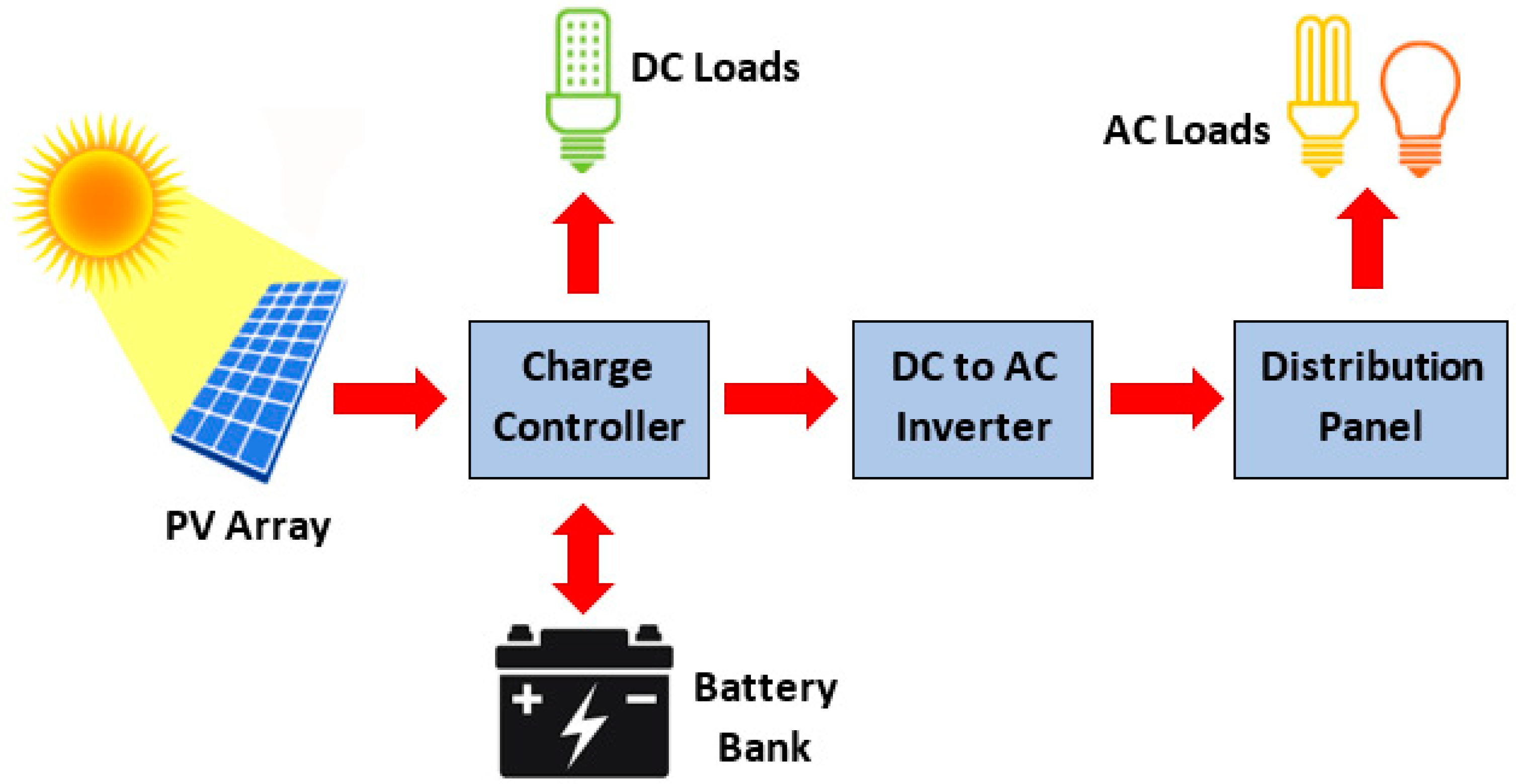
Standalone (off-grid) PV systems are used in rural areas where the national electricity grid is not accessible. These systems mainly consist of a PV array, charge controller and battery bank, as shown in Figure 1. Over the years, several types of standalone PV systems were introduced with novel power management and controlling strategies [3,4,5], although most of them have the same hardware. The charge controller is the most crucial part of a standalone PV system because it must extract, deliver and store maximum energy from the PV array into the battery bank to optimize the system efficiency. Modern commercial maximum power point tracking (MPPT) charge controllers employ switch-mode DC-DC converters to extract maximum available power from the PV array while stepping up or down the PV array voltage into the required voltage. The maximum power point (MPP) of the PV array is achieved by matching the instantaneous internal impedance of the PV array (under varying solar irradiance) to the load impedance by varying the duty ratio of the control pulse width modulation (PWM) signal of the DC-DC converter. This is accomplished by locating the MPP of the PV array using various MPPT algorithms. Constant voltage, current sweep, perturb and observe (P&O) and incremental conductance are the most common MPPT algorithms [6,7,8,9,10]. Conventional MPPT charge controllers have an average conversion efficiency of around 90% [11,12,13]. Most household electrical appliances require AC electricity. In order to drive AC loads, the system must employ a DC to AC inverter to convert the battery bank’s DC voltage into the required AC line voltage. Therefore, the overall system’s end-to-end (from source to load) efficiency while driving AC loads will be much less than that of the charge controller.

Figure 1.
Block diagram of a typical standalone photovoltaic system.
The recent development of supercapacitor (SC) technologies has enabled the use of SCs as an energy storage device for standalone PV systems [14,15]. Compared to batteries, SCs have higher power density and longer cyclic life, making them better suited for self-sustainable and low-maintenance systems [16,17,18,19,20,21]. When an empty capacitor charges to a voltage of by delivering charge , the capacitor stores of energy while wasting the same amount of energy in the total loop resistance, irrespective of the value of loop resistance [22]. This is a 50% energy loss compared with the electrochemical battery, where a battery stores an energy amount of . In addition, authors of [20] have studied the possibilities for impedance matching of a typical standalone PV system by connecting an SC bank at the output of the DC-DC converter, replacing the battery bank. Results indicate that tracking the MPP using the impedance matching technique is extremely difficult for such a system because of the rapid variation of the impedance across the SC bank with state of charge (SOC). However, authors of [23] have proposed a novel method of connecting an SC bank to RC circuit where SC is connected in series with a useful resistive load, leading to a higher end to end efficiency of the overall system. Reference [24] shows an application of this theory which uses a buck converter with a battery bank as the useful load in the capacitor charging loop to enhance system efficiency for a PV system.
This article discusses the design and development of a novel hybrid PV system consisting of a series-coupled SC with PV array and MPPT charge controller. The charge controller is connected to a battery bank, and the combination acts as the useful resistive load of the capacitor charging loop. Section 2 of this article provides a summary of SC assisted loss circumvention theory. Section 3 provides the conceptual background for developing the proposed PV system and its operational modes. Section 4 discusses the feasibility of the proposed hybrid PV system’s impedance matching technique under different operating modes. Finally, Section 5 presents the prototype implementation of the proposed PV system with SC assisted loss circumvention theory and experimental results that verifies the theoretical claims.
2. Supercapacitor Assisted Loss Circumvention Theory
Supercapacitor assisted loss circumvention theory is an extension of the typical resistor-capacitor (RC) circuit theory. This theory explains how to enhance the efficiency of a system using an SC charging loop consisting of a useful resistive load. This technique uses the advantage of a large time constant when a supercapacitor is connected to an RC circuit. Based on this concept, several SC assisted circuit topologies such as SC assisted light-emitting diodes (SCALED) [20], SC assisted low dropout regulator (SCALDO) [25] and SC assisted surge absorber (SCASA) [26] have already been developed. The fundamental background of this theory is summarized as follows.
As mentioned in Section 1, when the same amount of charge is pumped into a battery and an empty capacitor, the charging process of the capacitor wastes half of the total energy compared to the battery, irrespective of the value of total loop resistance. This is a fundamental observation of a typical RC circuit. SC assisted loss circumvention theory presented in the literature [23] suggests that for a case of charging a non-empty SC bank while connecting a useful load into the loop, the overall system’s efficiency can be enhanced. This is because the energy consumed by the useful load does advantageous work before being dissipated. Consider the capacitor charging circuit with useful load illustrated in Figure 2.
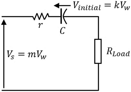
Figure 2.
Capacitor charging circuit with series-connected useful Load.
Using Figure 2, the efficiency, , of the system can be written as follows,
where , and are defined as the energy stored in SC bank, energy dissipated through the useful load, , and energy wasted in the loop resistances, , respectively. Here, includes the loop parasitic resistance and equivalent series resistance (ESR) of the SC bank. In Figure 2, and are defined as the pre-charge factor of SC bank and power supply over-voltage factor, respectively. When , SC bank reaches its pre-defined final voltage, which is denoted as . By analyzing the circuit for system efficiency, Equation (1) can be modified as follows [23],
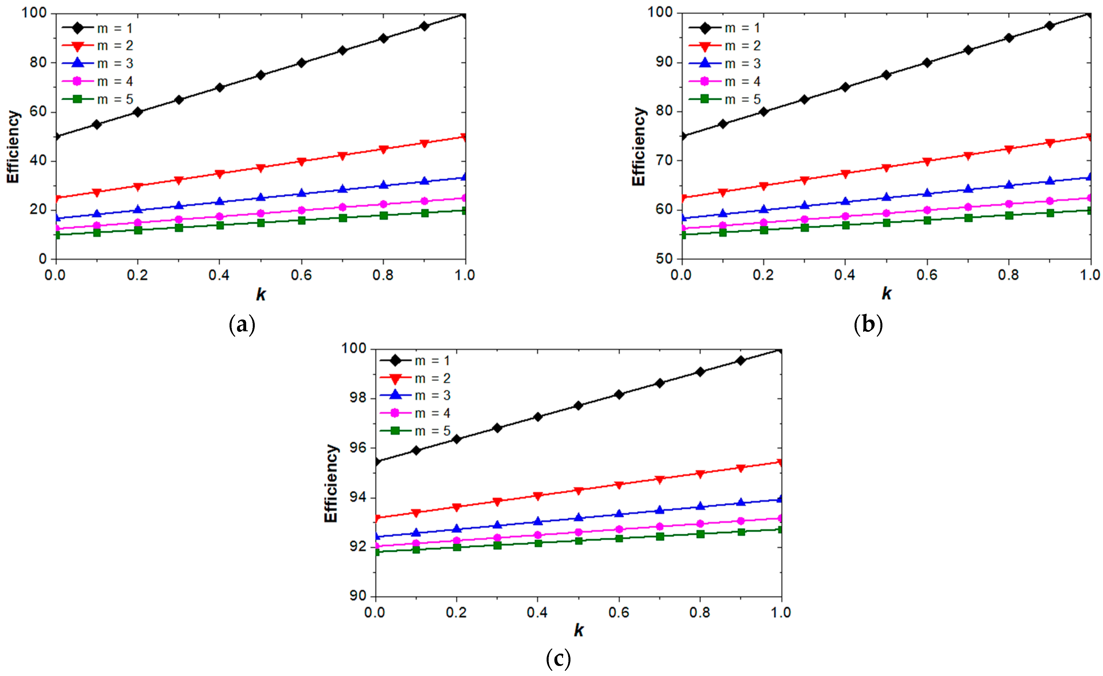
where . For the case of while and , we can obtain the fundamental efficiency, of a capacitor charging circuit as discussed in Section 1. Equation (2) suggests that if the capacitor is not allowed to discharge fully in a cycle (when ), system efficiency can be improved. As seen from Equation (2), can be enhanced by selecting proper values for and . When increases, the efficiency advantage increases significantly. This trend is shown in Figure 3a–c. These trends clearly show that the efficiency of an RC circuit can be enhanced by inserting a useful resistive load and a pre-charged SC into the RC circuit, as in Figure 2. Consequently, this concept can be applied to enhance the system efficiency of a PV system consisting of a series-coupled SC bank with a PV array and an MPPT charge controller. The following section demonstrates the development of the proposed PV system as an extension of the aforementioned loss circumvention theory.
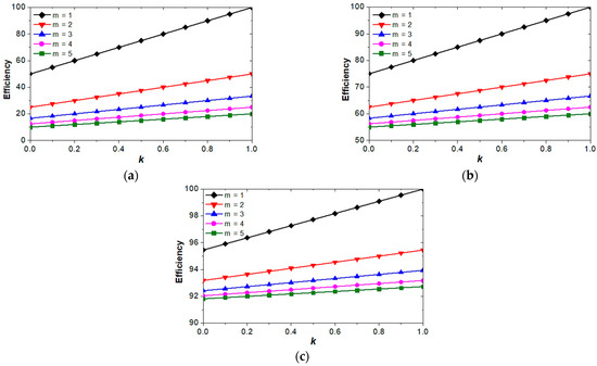
Figure 3.
Efficiency variation of the RC circuit vs. k and m: (a) at P = 0; (b) at P = 1; (c) at P = 10.
3. Development of the Proposed PV System Extending the Supercapacitor Assisted Loss Circumvention Theory
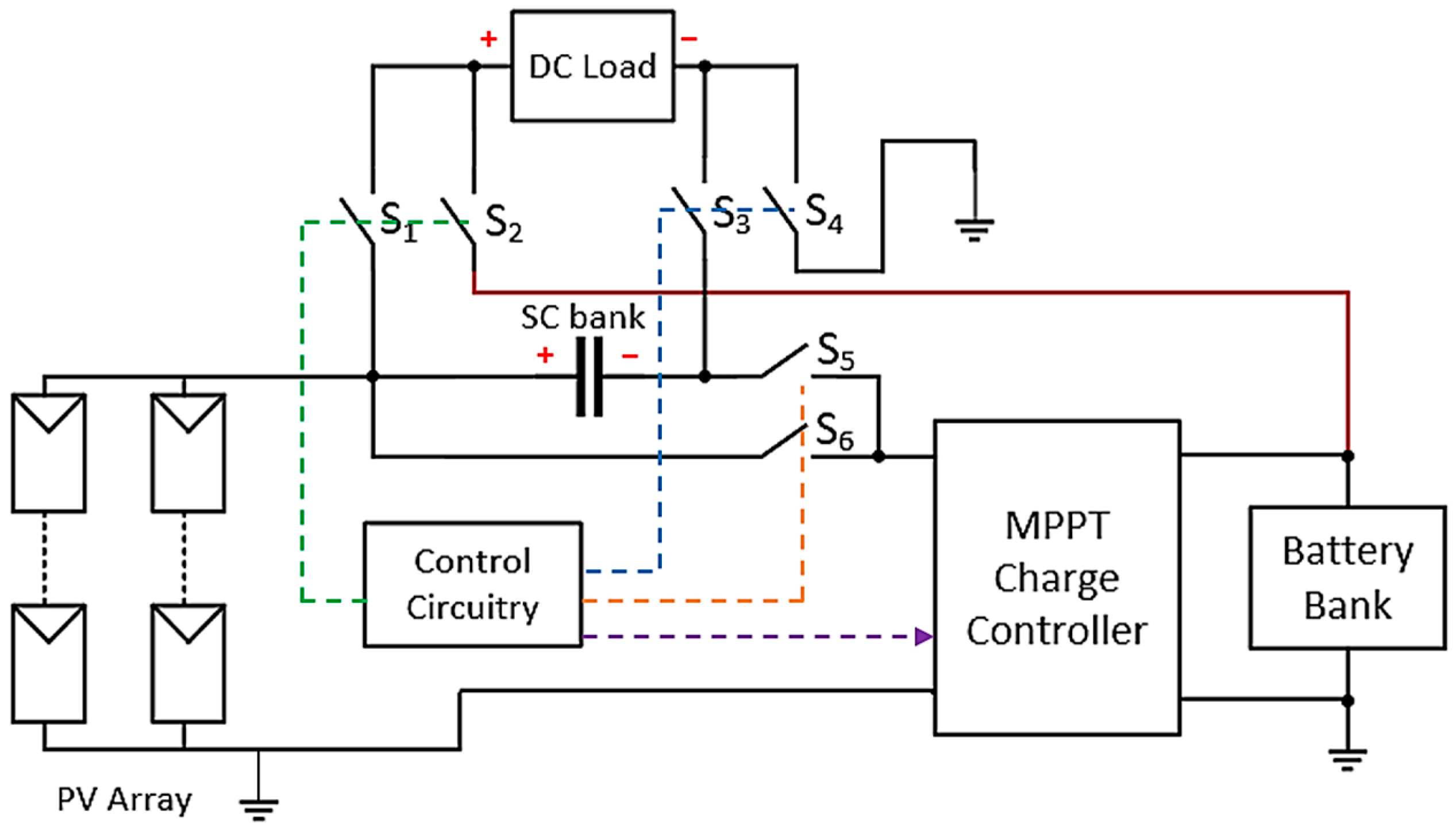
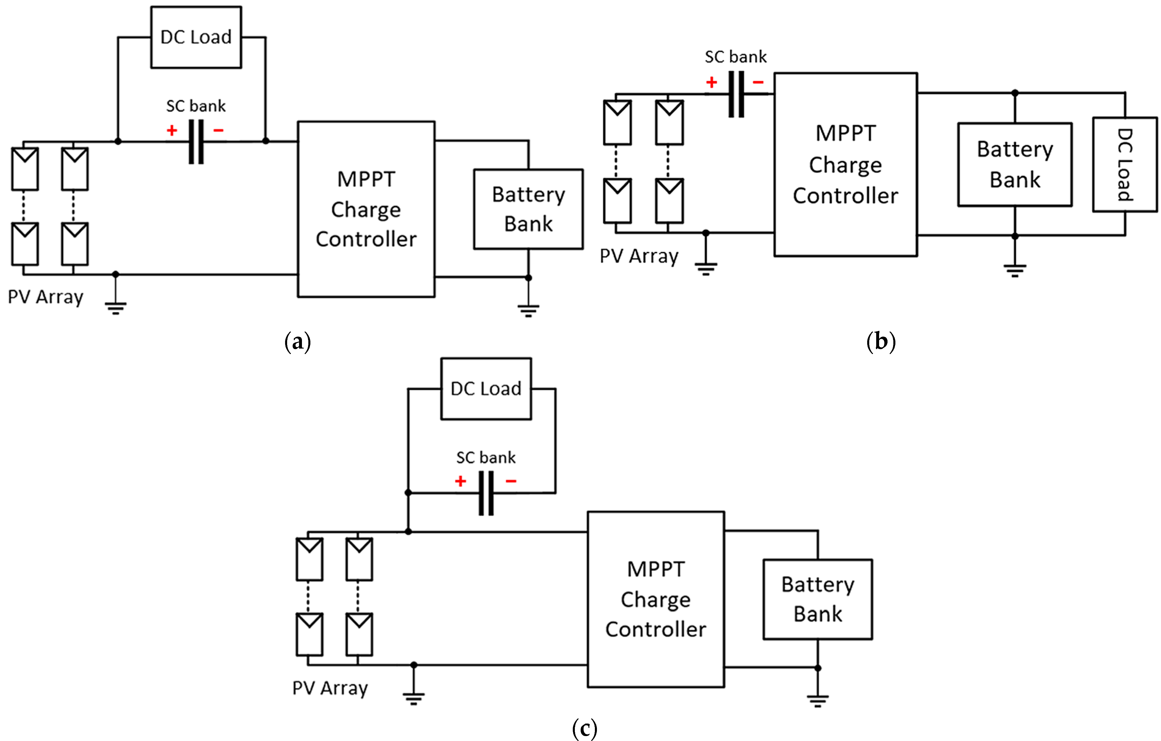
Figure 4 depicts a simplified block diagram of the proposed PV system. The proposed PV system has six switches , , , , and and they are switched “on” or “off” by the control circuitry of the system by assessing the PV array, SC bank and battery bank voltages. A DC load is introduced to the proposed system that implements a DC microgrid as a useful way to utilize the energy stored in the SC bank. It is essential to regularly use the stored energy so that the SC bank can be discharged to make it ready to store additional energy again. Depending on the switching algorithm that controls each switch’s “on” and “off” states, the system has three operating modes, as described in the text below.
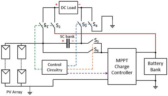
Figure 4.
Simplified block diagram of the proposed PV system.
3.1. Mode I: Neutral
Under this mode, the switches , and will be switched “on” while keeping the other switches “off”. This will implement the proposed SC-battery hybrid charging system while connecting the DC load in parallel with the SC bank. If the current output from the PV array is sufficient, the DC load will be driven directly by the PV array, while the excess current will flow through the SC bank, allowing the SC bank to charge. Then, the current will flow through the charge controller charging the battery bank. If there is a deficiency of current to drive the DC load, the SC bank will automatically buffer the excess current into the DC load, which will cause the SC bank to discharge slowly. The Block diagram of the system operating under this is shown in Figure 5a.
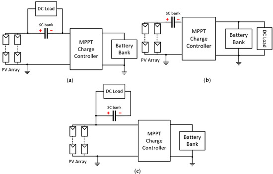
Figure 5.
System block diagram of each operating mode: (a) Neutral; (b) SC charge recovery; (c) SC bypass.
3.2. Mode II: SC Charge Recovery
If the voltage of the SC bank drops to its pre-defined minimum voltage because of the reduced input power while the system is operating in neutral mode, the DC load will be connected to the battery bank by switching and into “on” state and and into the “off” state while keeping the other switches in the same state. This will disconnect the DC load from the SC bank. Consequently, SC bank regains its charge, and when it is charged up to its pre-defined maximum voltage, the system will again be switched back into neutral operating mode. The Block diagram of the system operating under this mode is shown in Figure 5b.
3.3. Mode III: SC Bypass
If the SC bank reaches its pre-defined maximum voltage while the system is operating under the neutral mode, the switch will be turned “on” and will be turned “off” while keeping the other switches in the same state. This will connect the PV array directly parallel with the charge controller and the battery bank, similar to the typical systems. Now the DC load is totally powered by the SC bank, which causes the SC bank to discharge rapidly. When the SC bank is discharged to its pre-defined minimum voltage, will be switched back to “on” state while switching “off” . This will switch the system back into neutral mode. The system block diagram of this mode is shown in Figure 5c.
Table 1 summarizes the state of switches under each operating mode of the system. In all of the modes, it has been considered that the system is operating in the daytime. However, the SC bank can be fully discharged at night because the PV array is not generating power. Therefore, the system will be turned off at night, and all the loads can be connected to the battery bank, similar to the typical systems.

Table 1.
State of each switch under each mode of operation.
The overall operation of the designed system can be continued by switching the system into different operating modes. In neutral mode, since the DC load is driven directly by the PV array, charging, discharging and conduction losses will be minimized, enhancing the system’s efficiency. Another advantage of the proposed system is that when there is not enough current from the PV array, the SC bank will automatically buffer the DC load, which does not require any additional switching or special attention. Therefore, the switching losses are minimized. On the other hand, similar to the typical systems, a DC-AC inverter can be connected to the battery terminals to drive the AC loads using this system. With all these improvements, the proposed PV system leads to achieving very high system efficiency.
Tracking the MPP of the PV array is also an essential feature for a PV system. Even if the efficiency of the system is high, a PV system must be able to track the MPP if otherwise, maximum available power generated by the PV array will not be utilized. The following section theoretically investigates the feasibility of adapting typical impedance matching technique for maximum power transfer of the proposed system. To the best of the authors’ knowledge, such a study was not found in the literature for a proposed type of PV system.
4. Theoretical Investigation of MPPT for the Proposed System
In typical PV systems, the MPP of the PV array is achieved by matching the instantaneous internal impedance of the PV array (under varying solar irradiance) to the load impedance by varying the duty ratio of the DC-DC converter’s PWM control signal. This section investigates the feasibility of using the impedance matching technique for maximum power transfer of the proposed PV system operating under each mode, starting from the theoretical explanation of impedance matching of a typical PV system.
4.1. MPPT Using Switch Mode DC-DC Converter
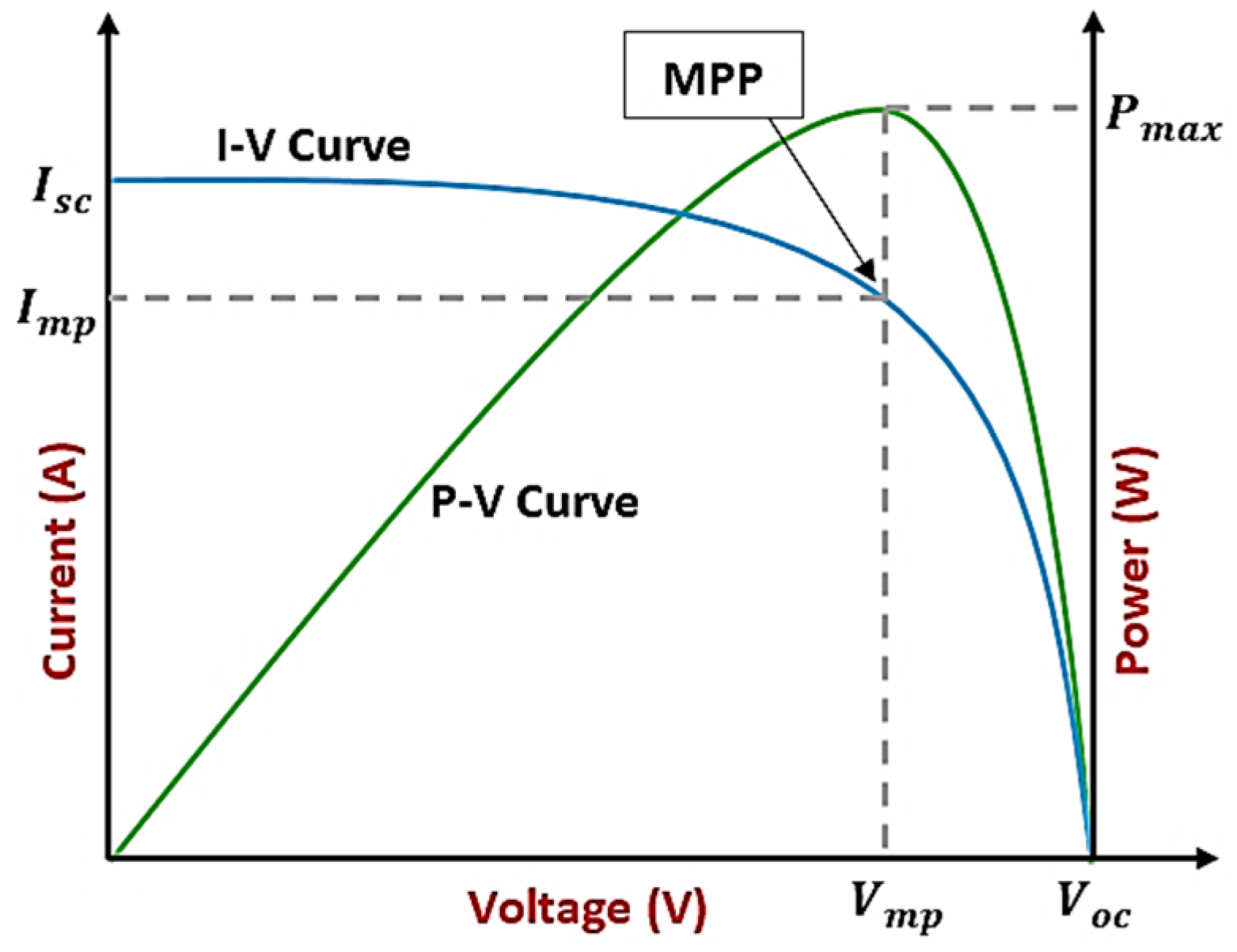
Figure 6 illustrates the current-voltage (I-V) and power-voltage (P-V) characteristics of a typical PV cell or array. , , and of Figure 6 are defined as open-circuit voltage, short-circuit current, the voltage at MPP and current at MPP, respectively. The MPP is the optimal operating point at which the PV array generates maximum electrical power. Under any operating condition, a PV system must operate at this point to extract the maximum available power from the PV array.
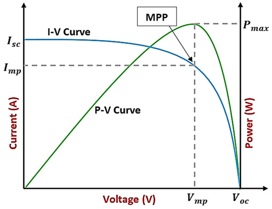
Figure 6.
I-V and P-V characteristics of a PV array.
As stated in the maximum power transfer theorem in electrical circuits, to transfer maximum power from a source with finite internal resistance to an external load, the resistance of the load must be equal to the internal resistance of the source as viewed from its output terminals. Therefore, to transfer the maximum amount of power generated by a PV array to an external load, the value of the instantaneous internal resistance of the PV array must be matched to the load. Hence, the resistance of the external load must also be able to vary continuously. In typical MPPT solar charge controllers, this is accomplished by continuously adjusting the duty ratio, , of the PWM control signal of the built-in DC-DC converter. There exist many types of MPPT algorithms [6,7,8,9,10], and they are all based on the impedance matching technique mentioned above.
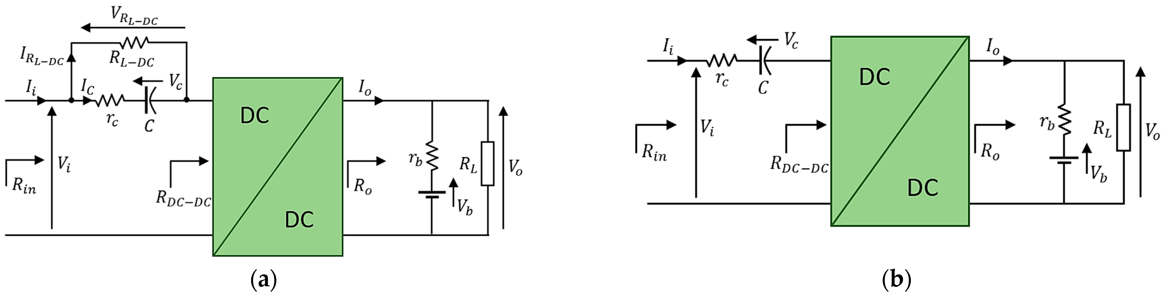
Switch mode buck or buck-boost converters are often employed in typical MPPT charge controllers. Consider the case of using a buck converter for the impedance matching operation of a standalone PV system. Figure 7 illustrates block diagram of a DC-DC converter, including a battery bank and a load connected to its output. , , , and depict in Figure 7 are defined as input current, output current, input voltage, output voltage and voltage of the battery bank, respectively. By considering Figure 7, Thevenin resistance, can be written as,
where is the internal resistance of the battery bank, and is the load resistance. can consists of several loads including a DC-AC inverter with an AC load. When a DC-DC buck converter is working under continuous conduction mode, it is equivalent to a DC transformer where the turns ratio of this equivalent transformer can be continuously controlled electronically in the range of 0–1 by controlling the duty ratio, , of the control signal [27]. Therefore, the relationships between and , and and can be written as [28],
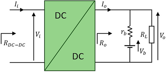
Figure 7.
Block diagram of a switch-mode DC-DC buck converter including a battery bank and a load connected to its output.
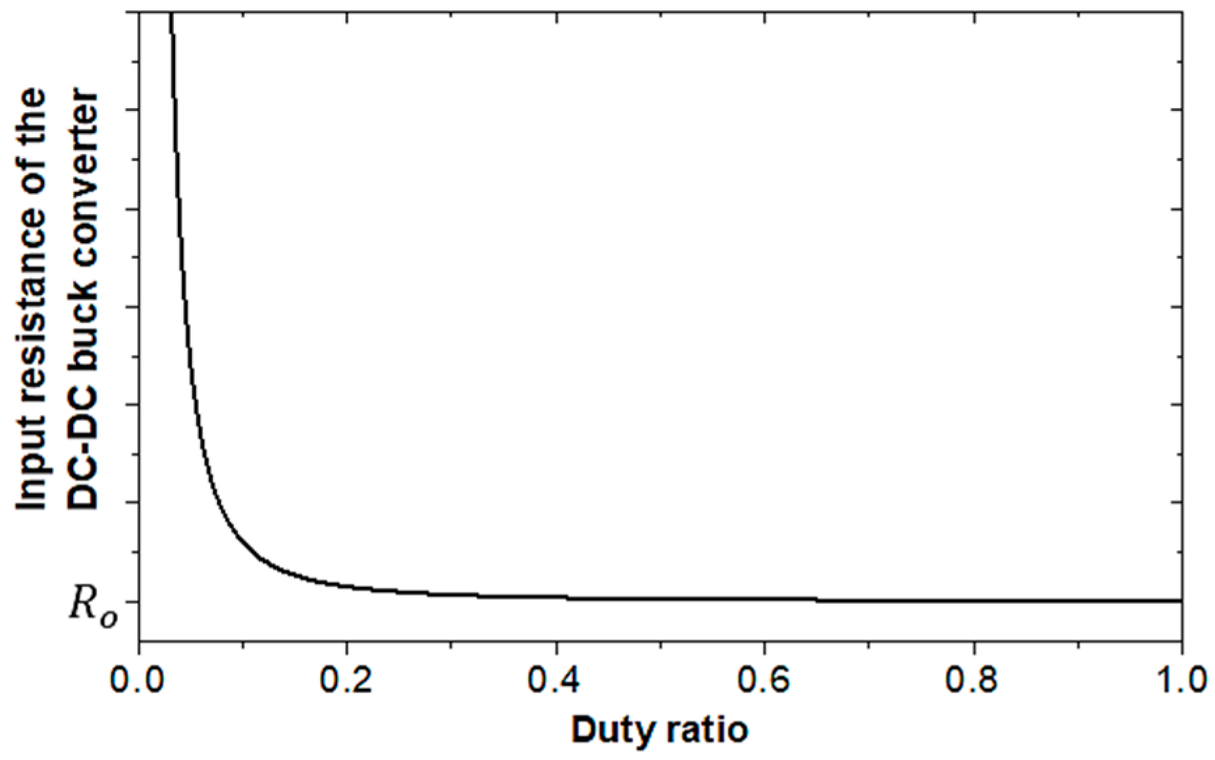
Under the assumption that the converter is lossless and always operates in continuous conduction mode, input resistance as seen from the input terminals of the buck converter can be deduced as [28],
Equation (6) clearly shows that the input resistance of the buck converter is a function of the duty ratio of the PWM control signal. Due to this relationship, when then (value of is minimized) and when then (value of is maximized). Therefore, the value of has a large variable span, as illustrated in Figure 8. This observation shows the possibility for the use of DC-DC converters in MPPT charge controllers.
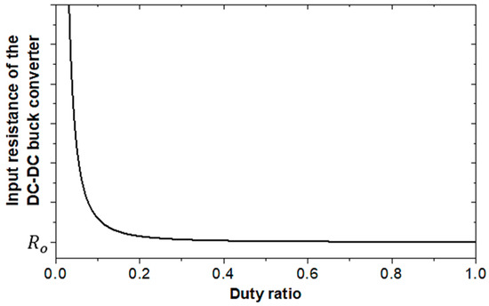
Figure 8.
Variation of the input resistance of the DC-DC buck converter with duty ratio of control PWM signal.
4.2. MPPT of the Proposed System
As discussed above, a battery bank connected at the output of a DC-DC converter allows simple impedance matching based on the effective resistive load seen by the solar panel. The same technique can be adapted for the SC bypass operating mode of the proposed PV system because under this mode, the PV array is directly connected with the charge controller bypassing the SC bank, while the SC bank solely powers DC load. Let us consider the case by case investigation of impedance matching for the remaining two operating modes of the proposed system as described in the below text.
4.2.1. Neutral Mode of the System
Consider Figure 9a, which illustrates the block diagram of the proposed system operating under neutral mode where the SC bank is connected in series between the DC-DC converter of the charge controller and output of PV array while DC load is connected in parallel with the SC bank. is the resistance of the DC load. , , and depict in Figure 9 are defined as the voltage of the SC bank (time-dependent), ESR of the SC bank, the capacitance of the SC bank and input resistance of the system as seen from the input terminals, respectively. Other symbols have the same meaning as in Section 4.1.
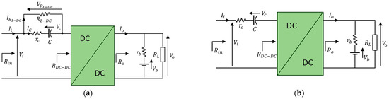
Figure 9.
Block diagram of the proposed system operating under: (a) Neutral mode; (b) SC charge recovery mode.
Using Ohm’s law, the voltage across the DC load (or SC bank), , can be written as,
Using the Equation (7) and Ohm’s law, an expression for the input current can be deduced as,
Using the Equation (8), final expression for can be deduced as,
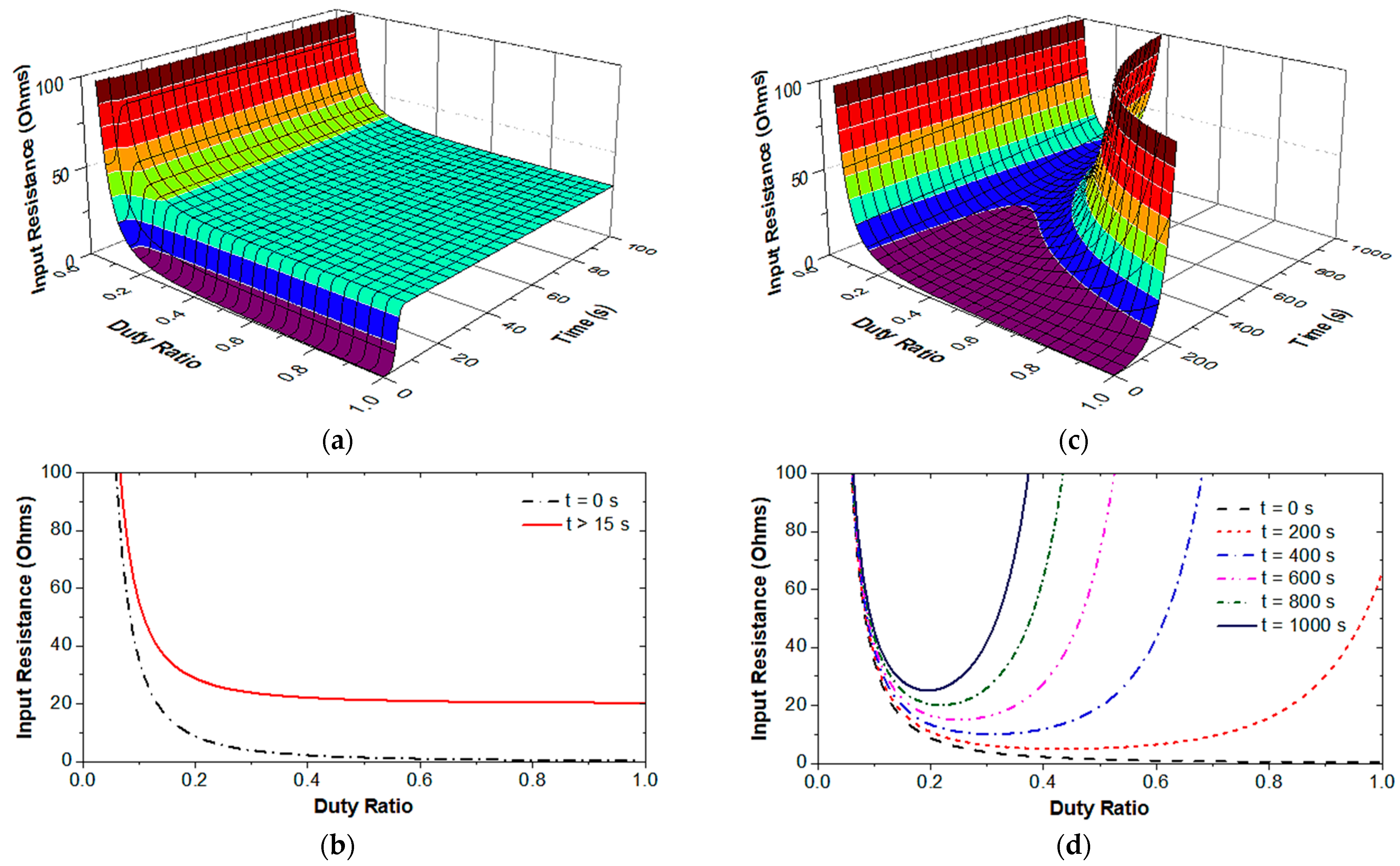
When considering the Equation (9), it is clear that for the case of the neutral mode of the proposed system, varies from to as goes from . Figure 10a,b show the behavior of input resistance of the system when it is operated under neutral mode.
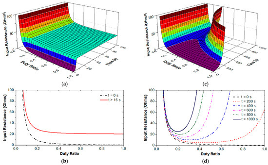
Figure 10.
Variation of input resistance of the system vs. time and duty ratio when the system is operated under: (a) Neutral mode; (b) Neutral mode at different values; (c) SC charge recovery mode; (d) SC charge recovery mode at different values. ( and ).
4.2.2. SC Charge Recovery Mode of the System
Consider Figure 9b, which illustrates the block diagram of the proposed system operating under SC charge recovery mode where the SC bank is connected in series between the DC-DC converter of the charge controller and the output of the PV array. If the initial voltage of the capacitor is zero, input current, , of the circuit shown in Figure 9b can be written as,
Using the Equation (10), can be deduced as follows,
As seen from the Equation (11), it is clear that is a function of both (time) and because is a function of . This implies that, in contrast with typical systems, the total resistance as seen from the input terminals of the system depends not only on the duty ratio of the PWM control signal but also on the SOC of the SC bank. When while , where this is the minimum value that could reach. In addition, when , regardless of the value of .
Compared to the typical case discussed in Section 4.1, the series connection of the SC bank with the PV array and DC-DC converter of the proposed system makes the input resistance of the system dependent on the SOC of the SC bank. For the case of neutral mode, the input resistance is a function of the resistance of the DC load as well. Therefore, the existing MPPT schemes have to be reconfigured to adapt them into the proposed SC-based PV system.
As seen from Figure 10c,d, because the exponential factor of the Equation (11) depends on elapsed time, the input resistance of the overall system increases rapidly with time. Therefore, to match the input resistance of the system to output resistance of the PV array at MPP by varying the duty ratio, , the input resistance of the system must have a finite value, less than that of the PV array at MPP for a particular maximum value of . So that can be further decreased by using the MPPT algorithm to match the input resistance of the system to the output resistance of the PV array at MPP. Therefore, maximum power point tracking using the impedance matching technique of the proposed system will be an impossible task if we allow the capacitor to fully charge during a cycle because the value of input resistance of the system will be very large regardless of the value of . However, for a case where the capacitor is not allowed to be fully charged during a cycle, MPP could be tracked because has a finite value less than the output resistance of the PV array. At the same time, the value of must have a minimum value at any given value for .
When considering the variation of under neutral mode as depicted in Figure 10a,b, is varying rapidly till the resistance across the SC bank reaches the value of . After that, the has the same variation with respect to as in the typical system but with having the minimum value of . Therefore, under this mode, the typical impedance matching can be implemented to track the MPP of the PV array if we carefully design the system. By considering above mentioned conditions, it is possible to match to the source resistance by varying as in a typical system for each operating mode of the proposed system. Therefore, it can be concluded that the typical MPPT can be adapted to the proposed system.
5. Development and Performance Analysis of a Prototype of the Proposed System
By utilizing the SC assisted loss circumvention theory and the investigation of impedance matching of the proposed system, a prototype system has been developed and analyzed. Table 2 shows the component values used for implementing the prototype system. The following two sections discuss the simulation of impedance matching and performance analysis of the prototype.
Table 2.
Component values of the prototype.
5.1. Simulation of Impedance Matching of the Prototype
The voltage of an energy storage device of a PV system must be maintained at a nominal value. For example, typical systems use batteries with a nominal voltage of 12 V or higher. For the case of connecting an SC bank into a PV system, the voltage of the SC bank must also be maintained at a nominal voltage. The developed prototype is a 12 V system, and therefore, for a given charge and discharge cycle of the SC bank, we could allow the SC bank to reach a voltage of 13.5 V as the upper threshold and 10.5 V as lower threshold keeping the SC bank’s nominal voltage at 12 V. This will help the system to operate smoothly. Since we are not charging the SC bank to its maximum capacity, this should help to track the MPP of the PV array of the proposed system.
Commercial SCs have lower ESR (0.1 to 100 mΩ) than the electrolyte capacitors (30 to 1000 mΩ), making SCs less dissipative. Therefore, the dissipative voltage across a series-connected SC could be negligibly small. The potential difference, , across an SC bank, can be large and only varying slowly because is inversely proportional to the capacitance. For a case of constant current charging, can be deduced as follows [22],
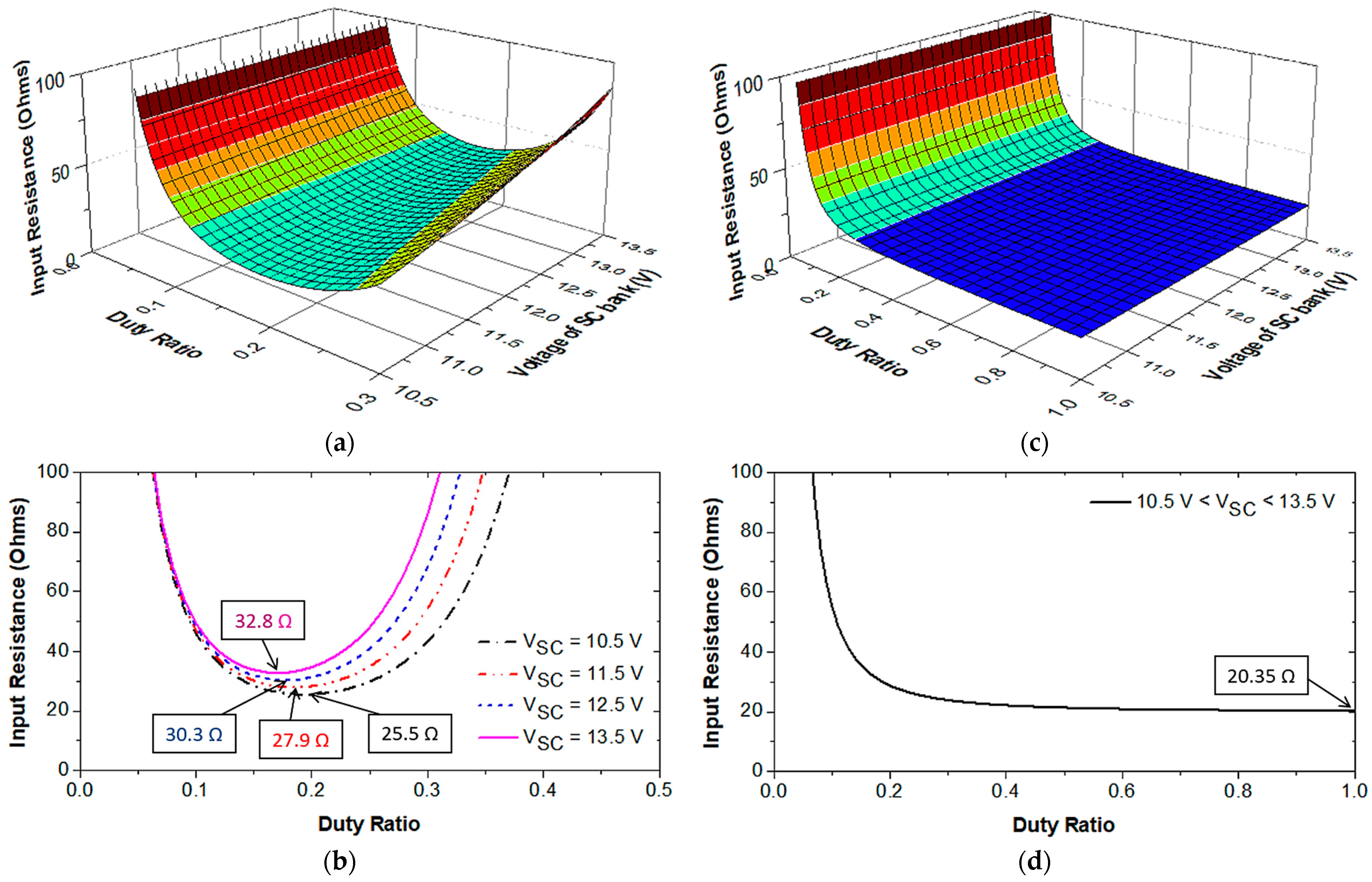
where is the time elapsed to increase the potential difference across the capacitor in volts and is the capacitance of the capacitor. Using the Equation (12) and theoretical investigation discussed in Section 4, the variation of with respect to the SOC of SC bank and duty ratio for the prototype system was simulated for neutral and SC charge recovery modes, and the results are depicted in Figure 11.

Figure 11.
Variation of input resistance of the prototype system vs. duty ratio and SOC of SC bank when the system is operated under: (a) SC charge recovery mode; (b) SC charge recovery mode at different values; (c) Neutral mode; (d) Neutral mode at .
In this simulation, the initial voltage of the SC bank was set to 10.5 V, and the simulation was run until it reached 13.5 V. As seen from Figure 11a,b, it is clear that when the SOC of the SC bank is maintained between prescribed levels, the minimum value of the input resistance of the system has the values of less than or very close to the value of the output resistance of PV array (32 Ω) at different duty ratios. Therefore, MPPT using the impedance matching technique for the prototype system working under SC charge recovery mode is possible, and it can be carried out by varying , similar to typical systems throughout maximum allowable charge and discharge voltage span of the SC bank. In addition, as seen from Figure 11c,d, for the prototype system working under the neutral mode, the minimum value of input resistance is 20.35 Ω which is less than 32 Ω. Therefore, the MPP of the PV array can be tracked by varying similar to the typical systems.
The above mathematical simulations have been conducted by assuming that the PV array is always operated at its MPP. However, the output power of the PV array will decrease with the reduced solar irradiance. Moreover, according to the typical PV array characteristics, the output impedance of the PV array at MPP increases with diminished solar irradiance. Therefore, can be further varied to match the impedance of the proposed system to that of the PV array to maximize the power transfer similar to typical systems.
5.2. Performance Analysis of the Prototype
Figure 12 shows the detailed block diagram and the experimental setup containing a prototype of the proposed system. All the switches in the switching network were designed by using power MOSFETs. To track the MPP of the PV array, the typical incremental conductance MPPT algorithm was used by implementing it on the in-built microcontroller of the control circuitry. Performance of the system was analyzed for all three operating modes of the system as follows. During the experiments, all the observations were taken while the battery was operated under the bulk charging mode.
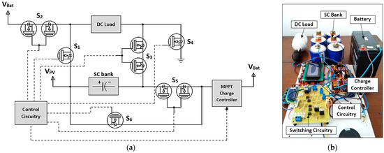
Figure 12.
System prototype: (a) Detailed block diagram; (b) Experimental setup.
5.2.1. Neutral Mode
When the system is operating under this mode, DC load is driven directly by the PV array when there is enough output current from it, and if not, the excess current required by the load is provided by the SC bank. The performance of the system under these two conditions is analyzed separately, and presented as follows.
1. DC load is driven directly by the PV array
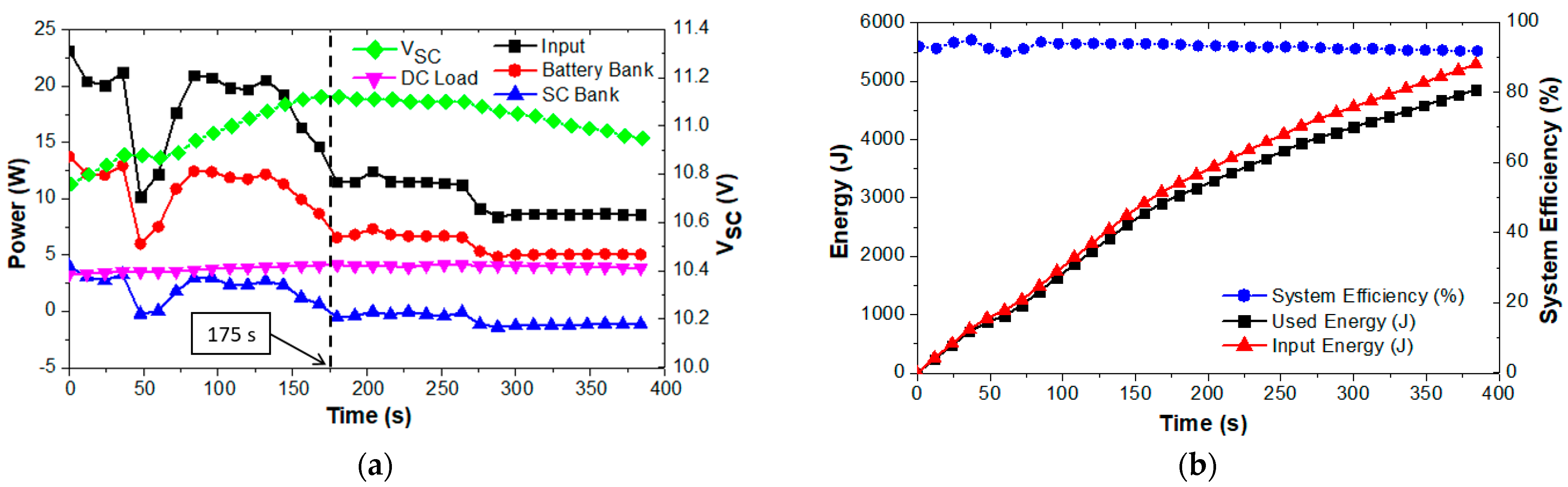
Figure 13 illustrates the variation of input power from the PV array, power delivered to the battery bank, SC bank and DC load, and voltage of the SC bank and input and used energy and system efficiency with respect to time during the experiment. It can be seen that the DC load has been driven directly by the PV array since there is enough current from the PV array, and excess current has flown through the SC bank, which has enabled it to charge slowly. As seen from Figure 13a, the system has extracted power from the PV array close to its MPP at reduced solar irradiance incident on the PV array. Figure 13b clearly shows that the average efficiency of around 96% has been achieved by the system.
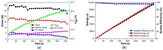
Figure 13.
Variation of: (a) Input power from the PV array, power delivered to battery bank, SC bank and DC load, and voltage of the SC bank; (b) Energy input, used energy and system efficiency vs. time when system is operating under Neutral mode while DC load is driven directly by PV array.
2. DC load is driven by the PV array while the SC bank provides excess current
In this case, due to the variation of the solar irradiance, the output current from the PV array is not sufficient to directly drive the DC load. However, since it is connected in parallel with the SC bank, the excess current required by the load is provided by the SC bank when necessary, causing the SC bank to discharge slowly. As seen from Figure 14a, the SC bank has increased its charge until the time reaches around 175 s of the experiment. After that, the voltage of the SC bank has reduced since the SC bank has provided excess current required to drive the load. Therefore, it is clear that the system has been able to work smoothly under varying solar irradiance while tracking the MPP of the PV array. According to Figure 14b, it can be seen that the average efficiency of around 92% has been achieved by the system.
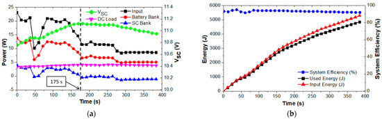
Figure 14.
Variation of: (a) Input power from the PV array, power delivered to battery bank, SC bank and DC load, and voltage of the SC bank; (b) Energy input, used energy and system efficiency vs. time when system is operating under Neutral mode while excess current required by DC load is provided by the SC bank.
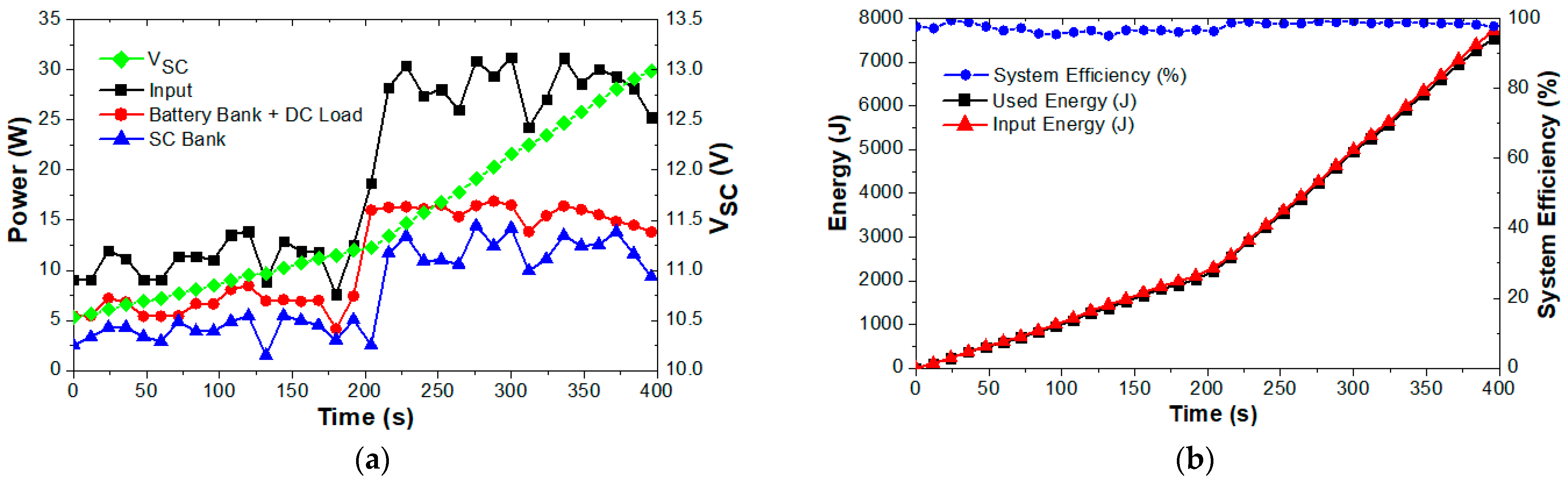
5.2.2. SC Charge Recovery Mode
The system is switched into this mode when the SC bank is discharged to 10.5 V while the system is operating under neutral mode. Since the SC bank is discharged, in order to drive the DC load, it is connected in parallel with the battery bank. As observed from Figure 15a, this has allowed the SC bank to charge rapidly. A portion of power delivered to the battery bank is utilized to drive the DC load, and if it is not enough to drive the load, the battery bank acts as a buffer by supplying the necessary power to the load. According to Figure 15b, it can be seen that the system has been able to achieve 98% average system efficiency during the experiment. This is around an 8% enhancement of efficiency as compared to commercially available typical PV systems [11,12,13].

Figure 15.
Variation of: (a) Input power from the PV array, power delivered to battery bank + DC load and SC bank, and voltage of the SC bank; (b) Energy input, used energy and system efficiency vs. time when system is operating under SC charge recovery mode.
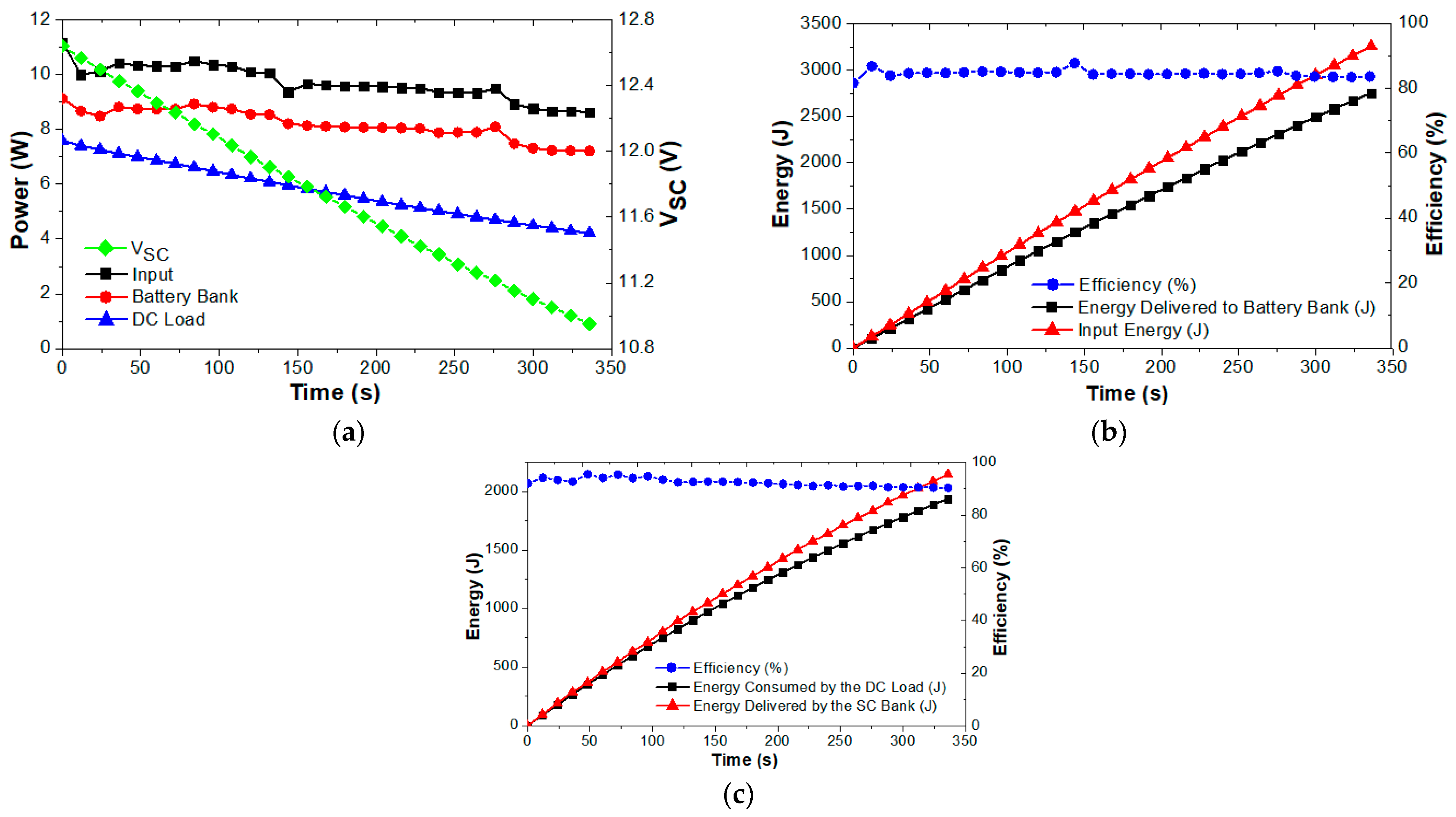
5.2.3. SC Bypass Mode
Under this operating mode, the DC load is directly powered by the SC bank, which has caused it to a rapid discharge, as shown in Figure 16a. PV array is directly connected with the charge controller and battery bank implementing a typical system. Therefore, when the system operates under this mode, the maximum available power of the PV array is directly transferred to the battery bank through the charge controller. As seen from Figure 16b, the system has achieved around 85% average efficiency. On the other hand, Figure 16c indicates that when the DC load is driven directly by the SC bank, the average efficiency of transferring the energy from the SC bank to the DC load is around 90%. Due to these lower efficiencies in this mode, the time that the system spends working under this mode during the day must be minimized as far as possible by carefully designing the system. Otherwise, the proposed system will not produce the anticipated outcomes.
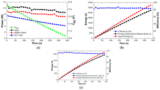
Figure 16.
Variation of: (a) Input power from the PV array, power delivered to battery bank and DC load, and voltage of the SC bank; (b) Energy input, energy delivered to battery bank and charging efficiency; (c) Energy delivered by SC bank, consumed by DC load and efficiency vs. time when system is operating under SC Bypass mode.
6. Conclusions
This article discusses a novel method that could be used to enhance the efficiency of a PV system using a supercapacitor bank as an auxiliary energy storage device. For the proposed system, theoretical and experimental validation of MPPT and efficiency enhancement techniques were carried out. From the results, it can be concluded that the efficiency of a PV system can be enhanced by the proposed technique while tracking the MPP of the PV array. A prototype of the proposed system has been developed. Experimentally it has been shown that when the system is operating in neutral mode, the system has achieved 96% and 92% efficiencies for the cases of high and low power output conditions of the PV array, respectively. When the system operates under the SC charge recovery mode, it has achieved 98% average efficiency. This is an 8% increment when compared to commercially available PV systems [11,12,13]. However, when the system is switched to the SC bypass mode, it has only 85% average efficiency. This happens because the system bypasses the SC bank and connects the PV array directly to the charge controller, implementing a typical standalone PV system. Finally, we envision that the results of this study would be available for commercial applications in the PV market very soon.
7. Patents
“Dynamic Power Management Technique for Supercapacitor-Battery Hybrid Photovoltaic Systems”, Sri Lankan Patent pending (21483).
Author Contributions
K.P. proposed the concept, designed the prototype model of the system, performed experimental work and wrote the manuscript. A.R., S.K. and N.K. supervised the project, participated in organizing the paper content, and editing the manuscript. All authors have read and agreed to the published version of the manuscript.
Funding
This research was funded by Accelerating Higher Education Expansion and Development (AHEAD) Operation of the Ministry of Higher Education of Sri Lanka, funded by the World Bank under the grant no. (6026-LK/8743-LK). The APC was funded by the University of Kelaniya, Sri Lanka.
Acknowledgments
Authors want to acknowledge the administrative and technical support provided by the research team of the Electronics Design and Innovation Centre, Department of Physics and Electronics of the University of Kelaniya, Sri Lanka.
Conflicts of Interest
The authors declare no conflict of interest.
References
- Guangzhou ZIC International Co., Ltd. Global PV Market Outlook 2019~2023. Available online: http://www.saroda.net/Index.php/News/company-161.html (accessed on 18 February 2020).
- Let’s Take Stock of Photovoltaics: Data and State of the Art. Available online: https://www.qualenergia.it/articoli/20170728-facciamo-il-punto-sul-fotovoltaico-dati-e-stato-dellarte/ (accessed on 18 February 2020).
- Mahmood, H.; Michaelson, D.; Jiang, J. Decentralized Power Management of a PV/Battery Hybrid Unit in a Droop-Controlled Islanded Microgrid. IEEE Trans. Power Electron. 2015, 30, 7215–7229. [Google Scholar] [CrossRef]
- Rosini, A.; Mestriner, D.; Labella, A.; Bonfiglio, A.; Procopio, R. A decentralized approach for frequency and voltage regulation in islanded PV-Storage microgrids. Electr. Power Syst. Res. 2021, 193, 106974. [Google Scholar] [CrossRef]
- Wu, D.; Tang, F.; Dragicevic, T.; Vasquez, J.C.; Guerrero, J.M. Autonomous Active Power Control for Islanded AC Microgrids with Photovoltaic Generation and Energy Storage System. IEEE Trans. Energy Convers. 2014, 29, 882–892. [Google Scholar] [CrossRef] [Green Version]
- Faranda, R.; Leva, S. A Comparative Study of MPPT Techniques for PV Systems. In Proceedings of the 7th WSEAS International Conference on Application of Electrical Engineering, Trondheim, Norway, 2–4 July 2008; pp. 100–105. [Google Scholar]
- Babaa, S.E.; Armstrong, M.; Pickert, V. Overview of Maximum Power Point Tracking Control Methods for PV Systems. J. Power Energy Eng. 2014, 2, 59–72. [Google Scholar] [CrossRef] [Green Version]
- Kumar, R.; Choudhary, A.; Koundal, G.; Singh, A.; Yadav, A. Modelling/Simulation of MPPT Techniques for Photovoltaic Systems Using Matlab. Int. J. Adv. Res. Comput. Sci. Softw. Eng. 2017, 7, 178–187. [Google Scholar] [CrossRef]
- Esram, T.; Chapman, P.L. Comparison of photovoltaic array maximum power point tracking techniques. IEEE Trans. Energy Convers. 2007, 22, 439–449. [Google Scholar] [CrossRef] [Green Version]
- de Brito, M.A.G.; Galotto, L.; Sampaio, L.P.; de Azevedo e Melo, G.; Canesin, C.A. Evaluation of the main MPPT techniques for photovoltaic applications. IEEE Trans. Ind. Electron. 2013, 60, 1156–1167. [Google Scholar] [CrossRef]
- Chowdhurt, S.A.; Mourshed, M. Off-grid electrification with solar home systems: An appraisal of the quality of components. Renew. Energy 2016, 97, 585–598. [Google Scholar] [CrossRef] [Green Version]
- Rezk, H.; Eltamaly, A.M. A comprehensive comparison of different MPPT techniques for photovoltaic systems. Sol. Energy 2015, 112, 1–11. [Google Scholar] [CrossRef]
- Rokonuzzaman, M.; Shakeri, M.; Hamid, F.A.; Mishu, M.K.; Pasupuleti, J.; Rahman, K.S.; Tiong, S.K.; Amin, N. IoT-Enepled High Efficiency Smart Solar Charge Controller with Maximum Power Point Tracking-Design, Hardware Implementation and Performance Testing. Electronics 2020, 9, 1267. [Google Scholar] [CrossRef]
- Kularatna, N.; Milani, K.; Round, W.H. Supercapacitor energy storage in solar application: A design approach to minimize a fundamental loss issue by partitioning the load and the storage device. In Proceedings of the IEEE 24th International Symposium on Industrial Electronics (ISIE), Buzios, Brazil, 3–5 June 2015; pp. 1308–1312. [Google Scholar]
- Kularatna, N. Energy Storage Devices for Electronic Systems; Elsevier: Amsterdam, The Netherlands, 2015. [Google Scholar]
- Galvin, M.E.; Hurley, W.G. Optimization of photovoltaic battery ultracapacitor hybrid energy storage systems. Sol. Energy 2012, 86, 3009–3020. [Google Scholar] [CrossRef]
- Fahad, A.; Soyata, T.; Wang, T.; Sharma, G.; Heizelman, W.; Shen, K. SOLARCAP: Supercapacitor buffering of solar energy for self-sustainable field systems. In Proceedings of the IEEE International SOC Conference, Niagara Falls, NY, USA, 12–14 September 2012; pp. 236–241. [Google Scholar]
- Kollimalla, K.; Mishra, M.K.; Narasamma, N.L. Design and analysis of novel control strategy for battery and supercapacitor storage system. IEEE Trans. Sustain. Energy 2014, 5, 1137–1144. [Google Scholar] [CrossRef]
- Glavin, M.E.; Chan, P.K.W.; Armstrong, S.; Hurley, W.G. A standalone photovoltaic supercapacitor battery hybrid energy storage system. In Proceedings of the 13th International Power Electronics and Motion Control Conference, Poznan, Poland, 1–3 September 2008; pp. 1688–1695. [Google Scholar]
- Jayananda, D.; Kularatna, N. Supercapacitor Assisted LED (SCALED) technique for renewable energy systems: A low-frequency design approach with short-term DC-UPS capability eliminating battery banks. IET Renew. Power Gener. J. 2020, 14, 1559–1570. [Google Scholar] [CrossRef]
- Kularatna, N.; Jayananda, D. Supercapacitor Based Long Time Constant Circuits. IEEE Ind. Electron. Mag. 2020, 14, 40–56. [Google Scholar] [CrossRef]
- Jayananda, D.; Kularatna, N.; Alistair Steyn-Ross, D. Design approach for Supercapacitor Assisted LED lighting (SCALED) technique for DC-microgrids. In Proceedings of the IEEE International Conference on Industrial Electronics for Sustainable Energy Systems (IESES), Hamilton, New Zealand, 31 January–2 February 2018; pp. 27–31. [Google Scholar]
- Aruayarathna, T.; Jayananda, D.; Kularatna, N.; Alistair Steyn-Ross, D. Potential of supercapacitors in novel power converters as semi-ideal lossless voltage droppers. In Proceedings of the 43rd Annual Conference of the IEEE Industrial Electronics Society, Beijing, China, 29 October–1 November 2017; pp. 1429–1434. [Google Scholar]
- Piyumal, P.L.A.K.; Ranaweera, A.L.A.K.; Kalingamudali, S.R.D.; Kularatna, N. Improving the Energy Storage of Standalone PV Systems while Enhancing the Charging Efficiency using Supercapacitors. In Proceedings of the 20th IEEE International Conference on Industrial Technology (ICIT), Melbourne, Australia, 13–15 February 2019; pp. 486–490. [Google Scholar]
- Gunawardane, K.; Kularatna, N. Supercapacitor-assisted low dropout regulator technique: A new design approach to achieve high-efficiency liner DC-DC converters. IET Power Electron. J. 2018, 11, 229–238. [Google Scholar] [CrossRef]
- Fernando, J.; Kularatna, N.; Round, H.; Talele, S. Implementation of the supercapacitor-assisted surge absorber (SCASA) technique in a partial surge protector. In Proceedings of the 40th Annual Conference of the IEEE Industrial Electronics Society (IECON), Dallas, TX, USA, 29 October–1 November 2014; pp. 5191–5195. [Google Scholar]
- Mohan, N.; Undeland, T.M.; Robbins, W.P. Power Electronics: Converters, Applications and Design, 3rd ed.; John Wiley & Sons Inc.: Hoboken, NJ, USA, 2002. [Google Scholar]
- Hart, D.W. Power Electronics; McGraw-Hill Education: New York, NY, USA, 2010. [Google Scholar]


Publisher’s Note: MDPI stays neutral with regard to jurisdictional claims in published maps and institutional affiliations. |
© 2021 by the authors. Licensee MDPI, Basel, Switzerland. This article is an open access article distributed under the terms and conditions of the Creative Commons Attribution (CC BY) license (https://creativecommons.org/licenses/by/4.0/).